1. Introduction
Edge detection is a fundamental operation in computer vision, serving as a cornerstone for numerous applications including object recognition, scene understanding, autonomous navigation, and infrastructure monitoring. In resource-constrained embedded systems, real-time edge detection presents significant computational challenges due to the intensive matrix operations required for convolution-based filtering. Traditional software implementations on general-purpose processors struggle to meet the stringent latency and energy constraints in resource-constrained embedded systems such as drones, mobile robots, and IoT vision devices. These systems demand specialized hardware acceleration strategies that balance computational throughput, power efficiency, and silicon area, requirements difficult to satisfy with conventional CPU or GPU architectures.
A particularly challenging scenario is infrastructure inspection using drones, which must navigate confined environments such as water supply and sewer pipe networks to detect structural defects. Currently, these inspections are performed using human vision, which carries a high risk of error due to the human factor. Real-time edge detection enables the automated identification of cracks, corrosion, and material degradation, reducing failures. Given the energy and processing constraints, the use of power-hungry embedded GPUs (5–10 W) is not feasible, making low-power hardware accelerators (<1 W) necessary while maintaining adequate performance.
Traditional software-based edge detection algorithms, although well-established in computer vision literature [
1], fail to meet the performance requirements of real-time embedded systems. Gradient-based operators execute sequentially on CPU cores, introducing latencies incompatible with processing constraints. Their computational complexity scales linearly with image resolution, making them unsuitable for embedded vision applications where power budgets and thermal envelopes impose hard constraints. FPGA-based acceleration has emerged as a promising alternative due to inherent parallelism and reconfigurability [
2]. Recent FPGA designs [
3] demonstrate efficient pipelined MAC implementations with time-division multiplexing for adaptive filtering, achieving substantial resource reductions through sequential processing. However, such single-MAC architectures with feedback-based operation are unsuitable for spatially distributed 2D convolution where multiple image windows must be processed concurrently. Existing FPGA implementations typically focus on isolated computational kernels without addressing system-level integration challenges such as efficient data distribution, inter-module communication, and scalable architectures for processing multiple image regions concurrently.
Systolic array architectures have demonstrated effectiveness for matrix-intensive operations in machine learning inference, particularly for convolutional neural networks [
4]. These structures exploit regular dataflow patterns, localized communication, and spatial reuse to achieve high computational density. Nevertheless, most systolic array implementations target cloud-based ASICs or datacenter accelerators where power budgets exceed 50 W, prioritizing raw throughput over energy efficiency and failing to address the area and power constraints characteristic of embedded systems. Furthermore, existing systolic implementations focus primarily on deep learning workloads, with limited exploration of their application to classical image processing tasks such as edge detection where simpler operators (Sobel) can achieve comparable results with lower hardware complexity.
Concurrently, Network-on-Chip (NoC) architectures have evolved to provide scalable communication fabrics for multicore and manycore systems. Solutions such as HopliteQ [
5] demonstrate priority-aware routing for FPGA overlay networks, while mesh-based AXI-MM interconnects [
6] improve bandwidth utilization in heterogeneous SoCs. Complex topologies including 3D NoCs with flexible routing [
7] enhance fault tolerance and adaptivity for large-scale systems. However, these NoC designs function primarily as generic data transport layers without integrating application-specific computational capabilities within the network fabric. This separation between communication infrastructure and computation introduces inefficiencies: data must traverse multiple hops between memory, NoC, and processing elements, increasing latency, energy consumption, and silicon area.
While architectural innovations address algorithmic and microarchitectural challenges, validating hardware designs down to physical implementation traditionally requires expensive commercial EDA tools (Cadence, Synopsys, Mentor), limiting accessibility for academic research. The complete IC design process is divided into two major stages: frontend (conceptual design, architectural specification, RTL coding, and functional verification through simulation and FPGA prototyping) and backend (physical design transforming RTL into manufacturable layout through synthesis, floorplanning, placement, clock tree synthesis, routing, and verification, ultimately generating the GDSII file ready for fabrication). Recent advances in open-source digital design flows have democratized ASIC development through tools such as OpenLane [
8] and OpenROAD [
9], automated RTL-to-GDSII flows, and the SkyWater 130 nm PDK [
10], the first open-source process design kit enabling fabrication-ready layouts. Successful tape-outs including RISC-V processors [
11,
12] and machine learning accelerators [
13] demonstrate the maturity of these flows. However, their application to domain-specific architectures, particularly heterogeneous systems combining communication fabrics (NoCs) with specialized accelerators (systolic arrays), remains underexplored, leaving a gap between architectural simulation and silicon-validated implementations for image processing applications.
The challenges outlined above reveal critical gaps in existing approaches for hardware-accelerated edge detection in embedded systems: (1) software-based methods cannot achieve real-time performance under sub-1W power constraints, (2) existing FPGA accelerators implement isolated kernels without integrated communication infrastructures for scalable coordination, (3) NoC architectures provide generic interconnects without application-specific processing integration, separating computation from communication and introducing data movement overhead, and (4) open-source design flows are underused for full ASIC validation, limiting reproducibility.
This work addresses these limitations by co-designing a hardware-accelerated edge detection architecture that unifies computation and communication within a homogeneous 2D-mesh Network-on-Chip, embedding systolic array processors directly within network tiles. Unlike conventional NoCs that function as passive interconnects, the proposed architecture integrates Sobel-based convolution accelerators at each node, enabling distributed parallel processing with efficient inter-tile communication. This co-design eliminates the separation between computational elements and communication fabric, reducing data movement, simplifying control logic, and improving energy efficiency. The architecture is validated through a dual-level implementation strategy demonstrating both functional correctness and physical feasibility.
The main contributions of this work are threefold. First, a tile-based NoC architecture embedding systolic array accelerators within network nodes is presented, demonstrating a scalable approach for distributed image processing in resource-constrained embedded systems. Second, the design is validated through dual-level implementation spanning both frontend and backend stages: (a) Frontend validation: a 3 × 3 mesh FPGA prototype with 32-bit data paths achieving 8.8 Gb/s throughput and 0.79 W power consumption at 100 MHz on a Zybo Z7-10 development board; and (b) Backend validation: a reduced 2 × 2 proof-of-concept with 14-bit word width implemented using the OpenLane RTL-to-GDSII flow targeting the SkyWater 130 nm PDK, demonstrating silicon manufacturability with timing closure at 100 MHz, 378 mW total power consumption, and full DRC/LVS compliance. Third, a complete open-source design flow from RTL specification to GDSII generation is contributed, enabling reproducible research in domain-specific hardware accelerators; while the primary application context is drone-based infrastructure inspection, the proposed accelerator is generalizable to any embedded vision system requiring real-time edge detection under power and area constraints.
The remainder of this article is organized as follows:
Section 2 provides background on edge detection fundamentals, detailing the Sobel operator, linear scaling method, and rationale for the chosen algorithmic approach.
Section 3 describes the proposed hardware architecture, encompassing both frontend and backend design.
Section 4 presents experimental validation results encompassing algorithmic performance metrics, FPGA hardware simulation statistics (frontend), and post-layout physical verification results.
Section 5 discusses identified limitations and future research directions. Finally,
Section 6 concludes by summarizing the main contributions and their implications for embedded vision systems.
2. Background: Edge Detection Fundamentals
2.1. Convolution for Edge Detection
The algorithm employed is based on the application of the Sobel operator combined with an additional linear-scaling stage, implemented over a parallel hardware processing architecture. The general procedure begins with a two-dimensional convolution operation, which combines two sequences to produce a third. In digital image processing, convolution involves applying a kernel or mask over an image to obtain a transformed result. Mathematically, the discrete two-dimensional convolution of an image
I with a kernel
K is defined as Equation (
1):
For edge detection, the Sobel operator was used. It employs two directional kernels that approximate the gradient of image intensity along the horizontal
and vertical
axes. Using separate kernels for each direction allows a more computationally efficient implementation. The kernels used are described in (
2) and (
3):
In the process, convolution is first carried out with and subsequently with , obtaining the horizontal and vertical gradient components, respectively. These results are combined to form the overall edge magnitude. Although a single unified kernel could be used to merge both directions, this simplification generally reduces edge-localization accuracy due to the loss of directional information.
To improve contrast and robustness under variable lighting conditions, such as those found inside water-supply and sewer pipelines, an additional transformation matrix
T was introduced to apply a linear-scaling operation to the convolution results. This transformation, defined in (
4), amplifies the dynamic range of pixel intensities and enhances depth perception [
14,
15,
16]:
The coefficients in matrix T were determined through engineering-guided empirical tuning using approximately 70 min of real-world pipeline inspection footage (≈126,000 frames at 640 × 480 resolution, 30 fps) captured across multiple infrastructure campaigns covering concrete, PVC, and cast iron pipes. Histogram analysis of representative frames identified pixel intensity distributions corresponding to structural defects (cracks, joints, surface irregularities), and coefficients were iteratively refined to enhance edge contrast in low-light regions while suppressing high-frequency noise. This calibration procedure reflects pragmatic engineering trade-offs appropriate for proof-of-concept hardware validation. The limited calibration dataset (confined to specific pipe materials and lighting conditions) constrains generalizability, and future production deployments would require expanded datasets with automated optimization and cross-validation to ensure robustness across diverse inspection environments.
Linear scaling adjusts the distribution of pixel values in grayscale images, increasing sensitivity to subtle intensity variations. It is important to emphasize that this transformation is implemented as a third convolution kernel (T) applied identically to
and
during sliding-window processing, rather than as a global intensity remapping operation. When applied together with the Sobel convolution, it enhances edge-detection precision at different depth levels by emphasizing low-contrast features that would otherwise remain undetected. The final edge map is obtained by combining both directional gradients and the linear-scaling component as shown in Equation (
5):
This procedure generates higher contrast and sharper contours, providing a more robust detection of structural discontinuities.
While algorithms like Canny [
17] offer robust edge detection through multi-stage processing (Gaussian smoothing, gradient computation, non-maximum suppression, hysteresis thresholding), they introduce irregular data dependencies and higher latency unsuitable for purely systolic hardware implementations. The hysteresis thresholding stage requires recursive connectivity analysis with unpredictable memory access patterns, complicating pipelined execution. In contrast, the proposed Sobel-based method with linear scaling offers a better balance between accuracy and hardware efficiency for real-time constraints. The regular convolution operations map naturally to systolic array architectures with deterministic dataflow, enabling efficient parallel processing. This method forms the foundation of the processing flow implemented in the NoC-based architecture designed for embedded vision applications.
While this work demonstrates the architecture using Sobel kernels, the design supports any 3 × 3 convolution-based operator that exhibits regular dataflow patterns, including Prewitt, Scharr, Roberts, Laplacian, Gaussian blur, and custom user-defined kernels. The systolic arrays perform generic multiply-accumulate operations on packet-embedded coefficients, enabling dynamic kernel switching without hardware reconfiguration. However, the architecture does not support operators with irregular data dependencies (e.g., Canny hysteresis thresholding, non-maximum suppression, morphological operations, or CNN pooling layers) that require non-deterministic memory access patterns incompatible with systolic pipelining.
2.2. Algorithmic Formalization
To ensure reproducibility and provide a formal specification of the edge detection method, this subsection presents the complete algorithm through structured pseudocode, processing flow diagram, and parameter configuration.
2.2.1. Algorithm Specification
The complete edge detection process is decomposed into three distinct algorithmic stages: (1) single-window convolution processing, (2) image decomposition into overlapping sliding windows, and (3) edge map reconstruction from distributed processing results.
Algorithm 1 details the core convolution operation applied to each 3 × 3 window. This procedure computes the three gradient components (horizontal, vertical, and linear scaling) through nested summation loops, followed by magnitude computation via the Euclidean norm. The algorithm accepts a single 3 × 3 pixel block and three convolution kernels as inputs, producing a scalar gradient magnitude as output. This operation maps directly to the systolic array processing performed at each NoC node.
| Algorithm 1: Single-Window Sobel Processing |
Input: window[3×3] ← pixel block (8-bit values) [3×3], [3×3], T[3×3] ← convolution kernels Output: magnitude ← gradient magnitude (14-bit or 32-bit) 1: // Horizontal gradient computation 2: grad_x ← 0 3: for i ← 0 to 2 do 4: for j ← 0 to 2 do 5: grad_x ← grad_x + window[i][j] × [i][j] 6: end for 7: end for 8: // Vertical gradient computation 9: grad_y ← 0 10: for i ← 0 to 2 do 11: for j ← 0 to 2 do 12: grad_y ← grad_y + window[i][j] × [i][j] 13: end for 14: end for 15: // Linear scaling computation 16: linear ← 0 17: for i ← 0 to 2 do 18: for j ← 0 to 2 do 19: linear ← linear + window[i][j] × T[i][j] 20: end for 21: end for 22: // Magnitude computation 23: magnitude ← 24: return magnitude |
Algorithm 2 formalizes the image decomposition procedure. It first applies zero-padding to create a 1-pixel border around the input image, ensuring that boundary pixels have complete 3 × 3 neighborhoods for convolution. The algorithm then extracts overlapping windows using a stride-1 sliding window approach, generating windows for an input image of dimensions . Each window is stored along with its center pixel coordinates, which are essential for subsequent reconstruction. This decomposition strategy preserves spatial continuity and eliminates reconstruction artifacts, as each output pixel corresponds to exactly one window’s central position.
Algorithm 3 specifies the reconstruction procedure for assembling the final edge map from processed gradient magnitudes. After distributed processing across NoC nodes, each window’s computed magnitude must be placed at its corresponding spatial location to reconstruct the complete edge image. The algorithm iterates through all processed magnitudes, retrieves their associated (x, y) coordinates from the position array, and assigns each value to the appropriate pixel in the output edge map. An optional normalization step scales the gradient magnitudes to the 8-bit range [0, 255] for visualization purposes, though the unnormalized values may be retained for subsequent processing stages that benefit from higher dynamic range.
| Algorithm 2: Image Decomposition into Sliding Windows |
Input: I[W×H] ← input grayscale image (8-bit, [0,255]) Output: windows[(W)×(H)][3×3] ← overlapping 3×3 blocks positions[(W)×(H)][2] ← center pixel coordinates 1: // Apply zero-padding (1-pixel border) 2: I_pad[W+2][H+2] ← zeros 3: for x ← 0 to W-1 do 4: for y ← 0 to H-1 do 5: I_pad[x+1][y+1] ← I[x][y] 6: end for 7: end for 8: // Extract overlapping windows with stride=1 9: window_count ← 0 10: for x ← 0 to W-1 do 11: for y ← 0 to H-1 do 12: // Extract 3×3 neighborhood centered at (x, y) 13: for i ← 0 to 2 do 14: for j ← 0 to 2 do 15: windows[window_count][i][j] ← I_pad[x+i][y+j] 16: end for 17: end for 18: positions[window_count][0] ← x 19: positions[window_count][1] ← y 20: window_count ← window_count + 1 21: end for 22: end for 23: return windows, positions |
| Algorithm 3: Edge Map Reconstruction from Processed Windows |
Input: magnitudes[N] ← gradient magnitudes from N windows positions[N][2] ← (x,y) coordinates for each magnitude W, H ← original image dimensions Output: E[W×H] ← reconstructed edge magnitude map 1: // Initialize output edge map 2: E[W][H] ← zeros 3: // Reconstruct by placing each magnitude at its position 4: for k ← 0 to N-1 do 5: x ← positions[k][0] 6: y ← positions[k][1] 7: E[x][y] ← magnitudes[k] 8: end for 9: // Optional: Normalize to 8-bit range [0,255] for visualization 10: max_val ← max(E) 11: if max_val > 0 then 12: for x ← 0 to W-1 do 13: for y ← 0 to H-1 do 14: E[x][y] ← (E[x][y] / max_val) × 255 15: end for 16: end for 17: end if 18: return E |
2.2.2. Processing Flow Diagram
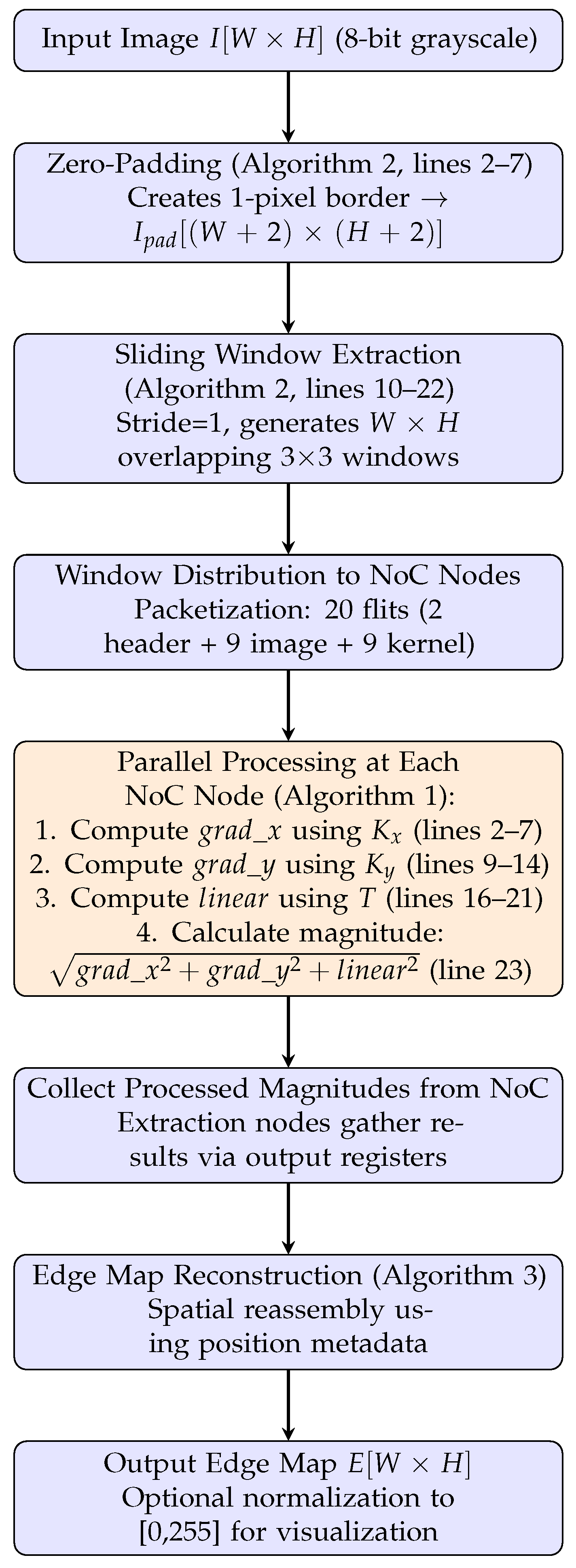
Figure 1 illustrates the complete data flow from input image acquisition to final edge map output. The process begins with the input grayscale image, which undergoes zero-padding (Algorithm 2, lines 2–7) to establish 1-pixel boundaries. The padded image is then decomposed into overlapping 3 × 3 windows using stride-1 sliding (Algorithm 2, lines 10–22), generating
windows that preserve spatial continuity.
These windows are distributed across the NoC nodes for parallel processing. Each node independently executes Algorithm 1, computing horizontal gradients (), vertical gradients (), and linear scaling (T) components before calculating the combined magnitude. The parallel execution across multiple systolic arrays enables real-time throughput, with each node processing windows asynchronously as packets arrive via the NoC routing fabric.
Processed gradient magnitudes are collected from the distributed nodes and forwarded to the reconstruction stage (Algorithm 3), where spatial reassembly produces the final edge map . The reconstruction process leverages the position metadata stored during decomposition to ensure correct spatial alignment. Optional normalization prepares the output for visualization or subsequent processing stages.
2.2.3. Parameter Configuration
Table 1 enumerates all algorithmic parameters, their values, and functional roles within the edge detection pipeline. Input images are 8-bit grayscale with typical resolution of 640 × 480 pixels for drone-based pipeline inspection applications. The FPGA prototype operates with 32-bit data paths to ensure sufficient precision during intermediate calculations, while the ASIC implementation reduces to 14-bit word width (justified in
Section 4.3) to meet area and routing constraints without compromising edge detection accuracy.
The convolution kernels (, , T) employ the standard 3 × 3 Sobel coefficients for gradient computation. The kernel detects horizontal edges via the pattern , while identifies vertical edges using . The linear scaling matrix T follows a similar vertical gradient structure with coefficients tuned empirically through histogram analysis of representative pipeline inspection images to maximize contrast in low-light regions without amplifying noise. Zero-padding with a 1-pixel border enables same convolution (output dimensions equal input dimensions), and stride-1 sliding ensures complete spatial coverage with minimal reconstruction overhead.
The packet structure (20 flits) encapsulates both image data (9 pixel values) and kernel coefficients (9 weights) within a single transmission unit, eliminating the need for kernel pre-loading at processing nodes and enabling dynamic kernel switching without reconfiguration overhead. This design choice trades 11.1% header overhead for simplified flow control and deterministic latency, as detailed in
Section 3.3.1. The FPGA prototype implements a 3 × 3 mesh topology with 9 processing nodes operating in parallel, while the ASIC proof-of-concept validates a reduced 2 × 2 cluster configuration constrained by physical design limitations discussed in
Section 4.3.
3. Proposed Hardware Architecture
The methodology employed in this work is divided into two complementary stages to validate the proposed edge detection architecture. The first stage (frontend) focuses on functional design and verification, as well as full system integration on an FPGA.
The second stage (backend) addresses physical feasibility through an ASIC implementation using open-source tools and design flows.
This two-level methodological approach connects the architectural design with its functional and physical validation, ensuring a comprehensive evaluation of the proposed system.
3.1. Image Decomposition and Block-Level Processing
To enable parallel execution within the NoC architecture, the input image is processed using overlapping 3 × 3 sliding windows with stride = 1, generating W × H windows (one per pixel) where W and H are the image width and height, respectively. Each window shares a 1-pixel overlap with its neighbors in all directions (±x, ±y), ensuring that every output pixel is computed from its complete 3 × 3 spatial neighborhood. To preserve spatial dimensions, the input image is zero-padded with a 1-pixel border before windowing, ensuring that boundary pixels also receive complete 3 × 3 neighborhoods and that the output edge map maintains the original W × H resolution. This approach matches the computational core of the systolic array, which performs matrix multiplications as its basic operation. The Sobel and linear-scaling kernels are applied to each window concurrently across multiple nodes.
This sliding window approach ensures that each processing element (PE) handles a localized 3 × 3 neighborhood of the image, reducing memory transfers and enabling simultaneous computation across all nodes. The fixed window size also simplifies synchronization and maintains a continuous data flow through the systolic array.
Each processed window generates the gradient magnitude for its central pixel, directly producing the corresponding position in the output edge map. Since windows overlap by construction, edge continuity is inherently preserved across the entire image without requiring explicit reconstruction or stitching of partial results. This distributed approach provides the same accuracy as a full-image convolution while achieving significantly lower latency and power consumption.
3.2. Systolic Array Implementation
The proposed hardware architecture integrates a systolic array accelerator within a 2D-mesh NoC to perform parallel convolution operations for edge detection, further boosting performance [
18,
19]. Each PE in the systolic array executes a multiply–accumulate (MAC) operation defined as in Equation (
6):
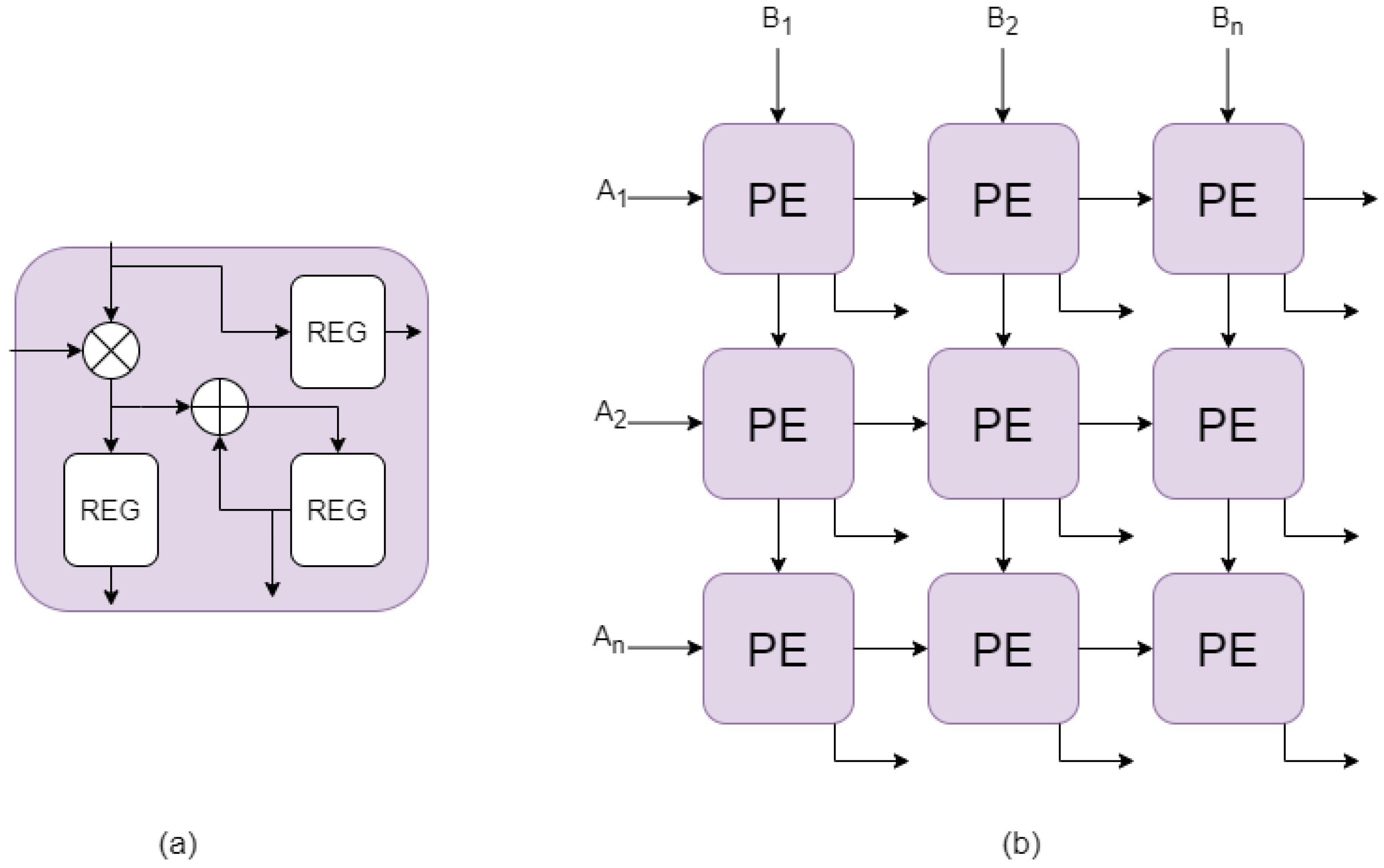
Matrices
A and
B are injected horizontally and vertically, respectively, propagating through the array in a synchronized flow that enables continuous computation (
Figure 2). This structure minimizes memory access overhead and latency [
20,
21], allowing efficient matrix multiplications critical for real-time edge detection [
21,
22].
3.3. NoC Architecture Design
To manage traffic and prevent saturation, the network implements cut-through switching with credit-based flow control. In this context, data flowing through the NoC is divided into packets, which are further segmented into smaller units called flow control units (flits). Flits represent the minimum storage and allocation units within the buffer. Typically, packets include header flits, which contain control information such as destination addresses and packet identification, and body flits, which carry the payload (data to be processed and already processed) through the network.
3.3.1. Packet Format in the NoC
Packets transmitted through the network have a fixed length, defined according to the homogeneous design of the implemented NoC architecture. This uniformity in packet structure simplifies flow control, optimizes buffer usage, and standardizes routing and processing operations throughout the network.
Each injected data packet is composed of 20 flits:
Header flits: The packet includes 2 header flits. The first manages routing and state control during the packet’s transit through the network (
Figure 3). The second is used in the output stage to identify the final storage location of the processed packet.
Data flits: Consisting of 18 flits that carry the useful information to be processed by the computing nodes. Specifically, 9 flits transport the 3 × 3 image window (9 pixel values) and 9 flits transport the corresponding 3 × 3 convolution kernel (, , or T), enabling each packet to carry all data required for a complete convolution operation without requiring kernel pre-loading or additional transmissions.
This packet structure yields a header-to-payload ratio of 2:18 (11.1% overhead) and an overall efficiency of 90%. The 10% overhead is justified by: (1) enabling self-contained convolution operations that eliminate the need for distributed kernel storage at each node, reducing memory requirements; (2) simplifying synchronization by bundling image data and kernel coefficients in a single atomic transmission; (3) supporting deterministic routing and credit-based flow control through dedicated header fields; and (4) maintaining a fixed packet size that simplifies buffer allocation and improves predictability of network latency. This design achieves higher payload efficiency than typical NoC packet formats (70–85%) while maintaining the flexibility to process different kernels dynamically. This design is not limited to Sobel operators—any 3 × 3 convolution kernel (Prewitt, Scharr, Laplacian, Gaussian, or custom coefficients) can be dynamically transmitted in packet payloads and processed without hardware modification, provided the operator maintains regular dataflow compatible with systolic pipelining.
Once processing is completed, the packet’s state is updated via a post-processing witness field within the header, and the destination and output address fields are swapped. This operation enables routing toward the extraction node, ensuring efficient transfer of the packet from the network to the output stage.
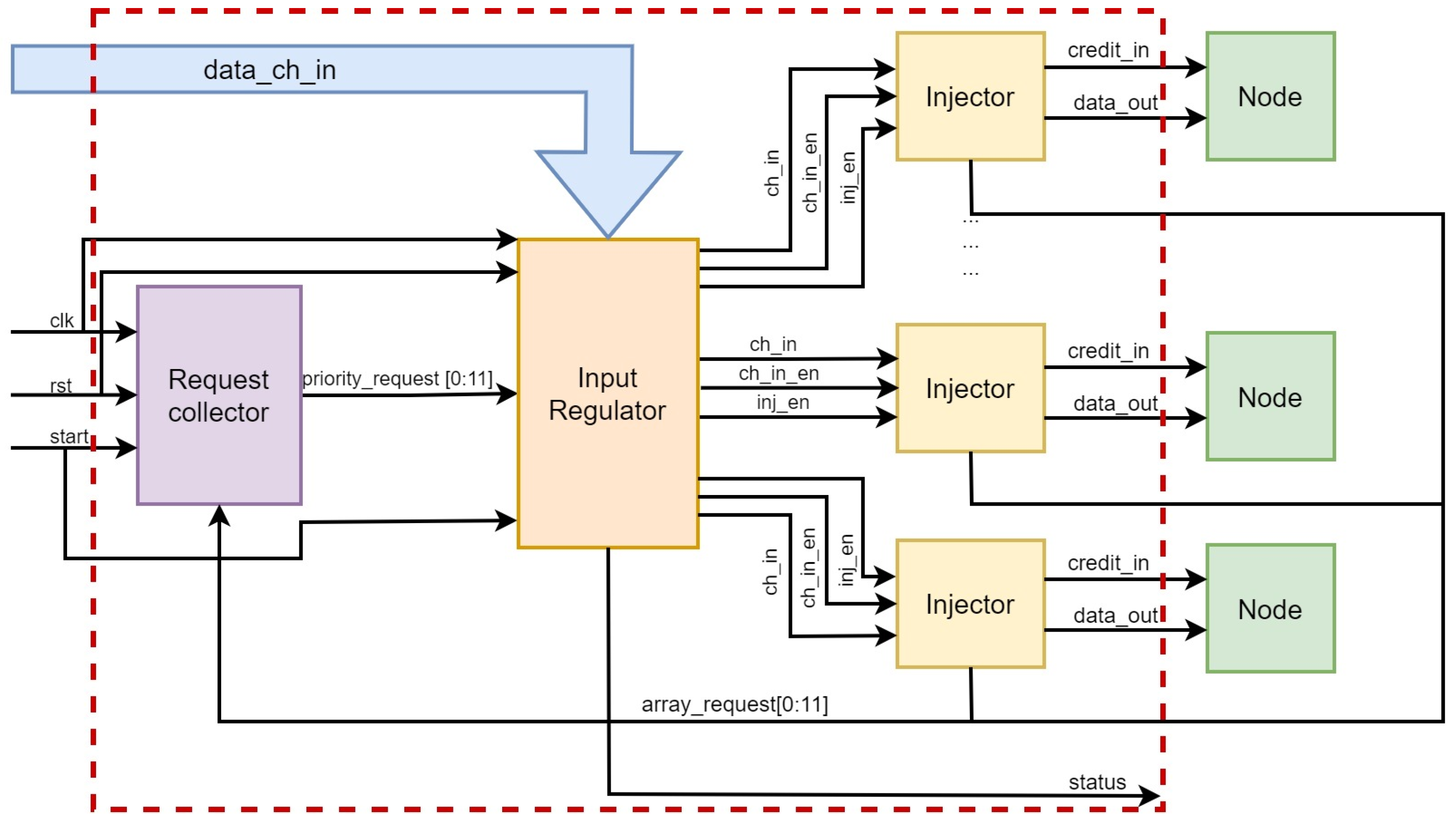
3.3.2. Input Stage
The input stage is responsible for injecting packets into the NoC and managing both the sequencing and arbitration of these injections. It is composed of three main modules:
Input Regulator: Temporarily holds the incoming packet until it is requested for processing.
Injectors (): Each injector monitors the availability of the NoC input channels. When space is available, it issues a request signal to initiate the packet transfer and establish communication with the NoC.
Request Collector and Arbiter: Central arbitration logic based on the West-First policy. It selects one injector among multiple simultaneous requests by prioritizing the lowest-order bit injector, and rotates the priority in subsequent cycles to ensure fairness.
Upon receiving an activation signal, all available injectors issue a request. The arbiter grants access based on a predefined hierarchy, ensuring a round-robin distribution of packet injections over time. Once the packet is injected, the
status signal is lowered to indicate readiness for the next packet.
Figure 4 shows the block diagram of the implemented.
3.3.3. Network Interface
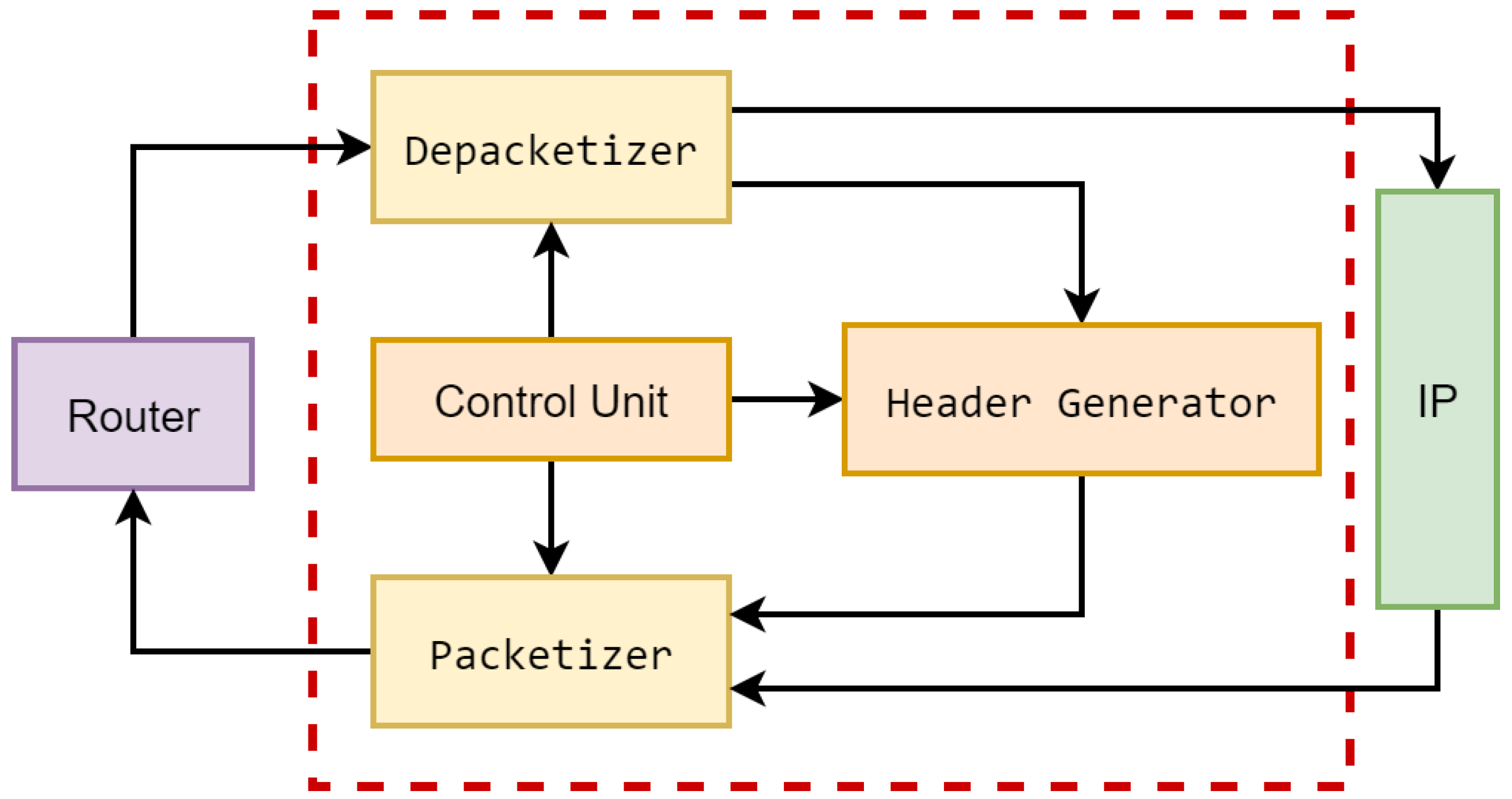
Network Interface (NI) serves as a bridge between the processing elements and the NoC. The implemented NI consists of three main components:
Depacketizer: Receives packets from the network and converts them into the working format used by the IP module.
Header Generator: Modifies the post-processing flag field to indicate to subsequent routers that the packet has already been processed, preventing its re-entry into other IPs along the route. It also swaps the destination and output fields in the header flit to properly route the packet to its final output.
Packetizer: Integrates the processed data along with the header information, forming a properly formatted packet to be re-injected into the network.
The NI is controlled by a finite state machine that synchronizes communication between the accelerator and the NoC, supporting flow control and backpressure management.
Figure 5 shows the block diagram of the implemented NI.
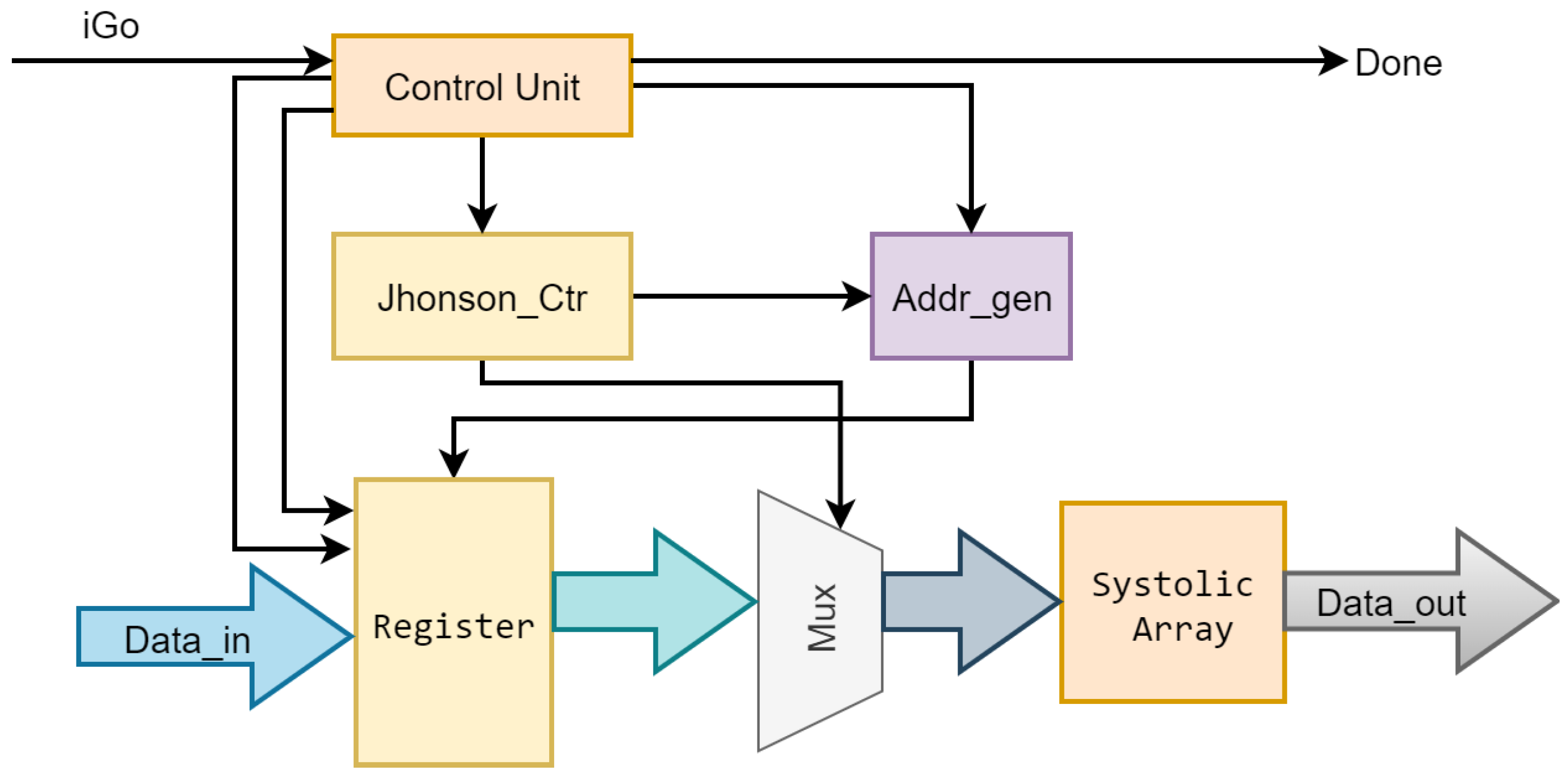
3.3.4. Hardware Accelerator
The hardware accelerator, illustrated in
Figure 6, is composed of six main modules:
Control unit: Manages the computation flow using a finite state machine (FSM) with three stages: IDLE, READ, and MULT.
Johnson counter: Generates a control sequence to enable valid data injection through the multiplexers.
Address generator: Computes the memory addresses of matrix elements to control data access and sequencing.
Input register: Temporarily holds matrix segments A and B received from the NI.
Multiplexers: Select between real data and control zeros, managing the injection pattern into the systolic array.
Processing core (SA): Executes the multiply-and-accumulate operations for localized matrix blocks.
The accelerator divides large matrices into smaller blocks for localized multiplications. Each row-column block pair is processed within the systolic array to generate the output segment. To ensure proper injection, the Johnson counter and address generator control both timing and memory access. Address Equations (
7) and (
8) determine data positions within the input register.
3.3.5. Routing and Transmission
Once injected, packets are routed and processed through a scalable NoC infrastructure designed to support high-throughput communication. The NoC uses a two-dimensional mesh topology where each packet carries explicit destination coordinates (x, y) in its header, directing it to a specific processing node. The implemented workload-distribution mechanism follows a first-come-first-served (FCFS) policy at each node, ensuring deterministic processing order while West-First routing provides the path adaptability needed to handle network congestion.
When a packet arrives at its designated destination node, the router inspects the post-processing witness flag in the header: if the flag is cleared (indicating an unprocessed packet), the Network Interface attempts delivery to the local systolic accelerator; if the accelerator is busy, credit-based flow control signals back-pressure, causing the packet to wait in the router’s buffer until the accelerator becomes available. Once processed, the NI sets the witness flag and swaps the destination and output address fields, enabling deterministic routing toward extraction nodes. This mechanism ensures that each packet is processed exactly once at its assigned coordinates while maintaining deadlock-free operation.
The routing algorithm implemented within this NoC is West-First (WF) [
23], a partially adaptive algorithm that avoids circular deadlock by restricting certain turns in the network. The West-First algorithm operates by prohibiting any turn from a direction other than west into the west direction, effectively eliminating cyclic channel dependencies that could lead to deadlock. Under this policy, packets must first complete all westward hops before being allowed to turn north, south, or east. Once routing in non-west directions begins, the packet may adaptively choose among the remaining three directions based on local congestion and availability, but is prohibited from turning west again. This routing restriction ensures deadlock freedom while maintaining partial adaptivity, allowing the network to balance traffic across multiple paths when congestion occurs. The policy prevents cyclic dependencies that can cause network lockup, ensuring efficient and reliable transmission of the processed image data [
24,
25].
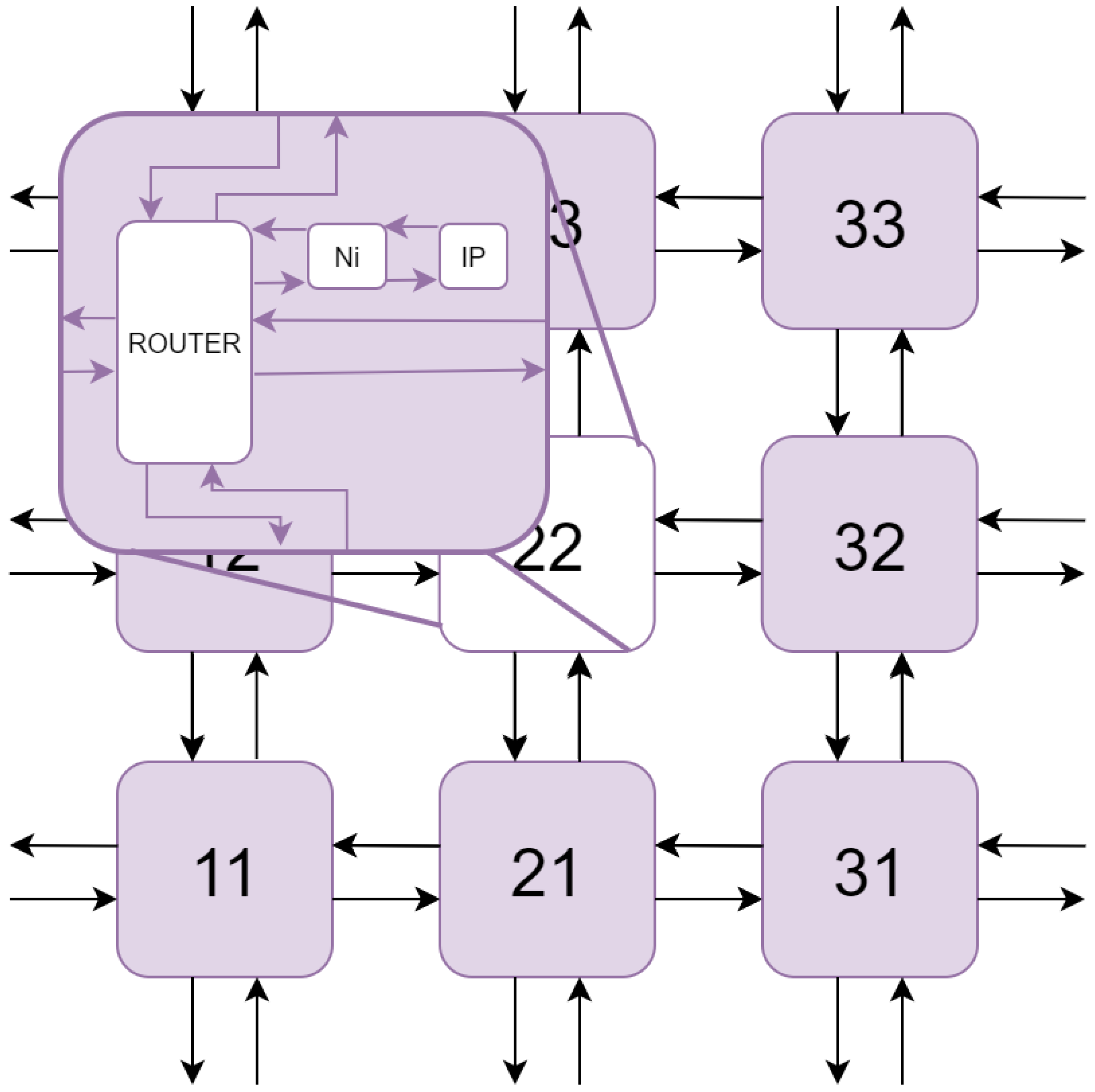
Each node contains a dedicated IP core (the systolic accelerator), a NI that handles communication between the router and the accelerator, and a router with four bidirectional ports connecting to neighboring nodes (north, south, east, and west), plus one NI port that uses credit exchange.
The router’s datapath handles packet traversal, while the control path determines routing. A two-stage critical path first stores and computes the route, then configures the crossbar and forwards flits, allowing zero-load packets to advance to the next node in a single clock cycle.
The general integration diagram of the NoC is shown in
Figure 7.
3.3.6. Output Stage
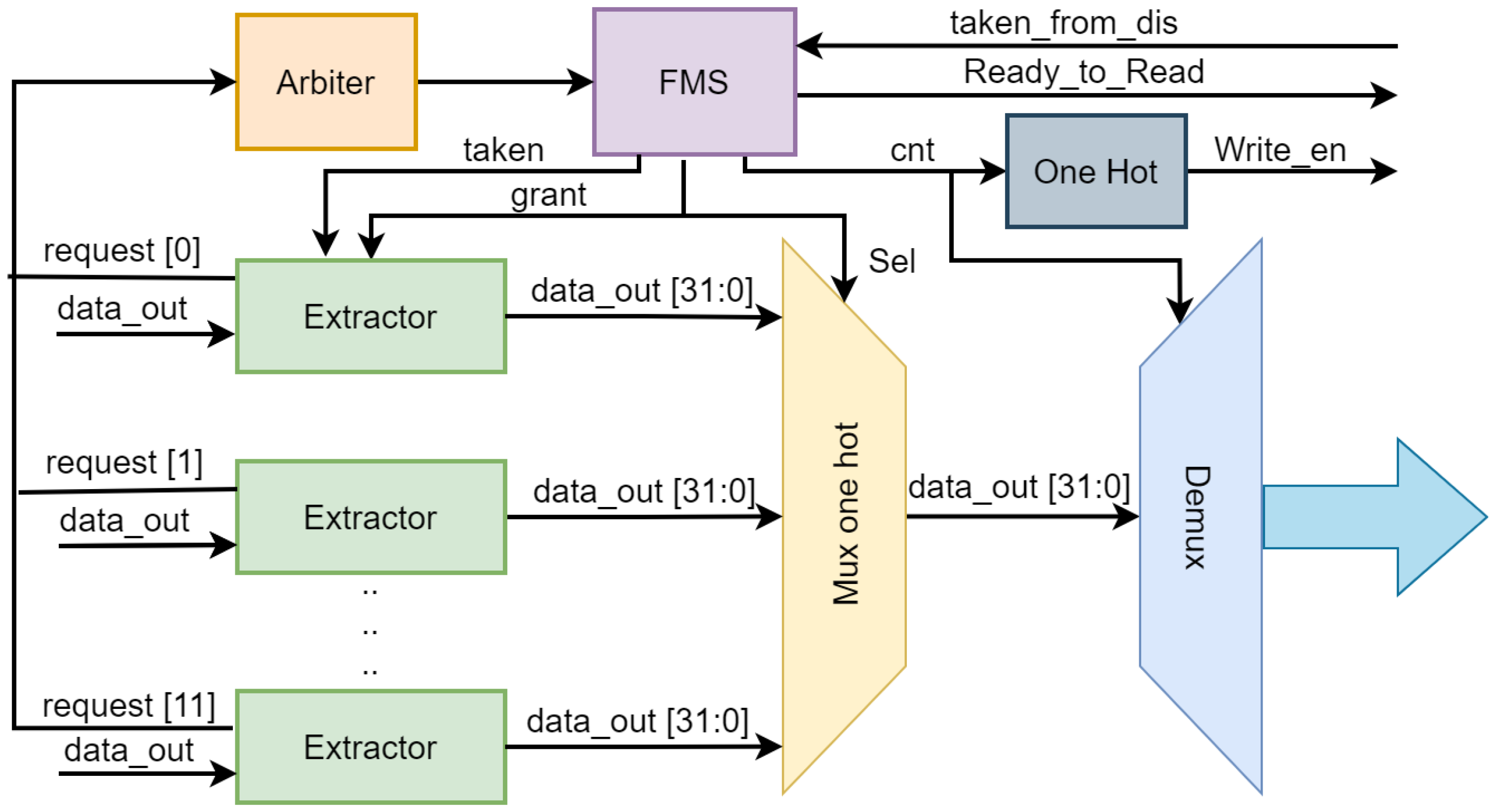
The output stage is responsible for the extraction and dispatch of processed packets from the NoC. Its main components are:
Extractors: Directly connected to the NoC output ports. They monitor for packets ready to exit and assert a request signal when such packets are available.
Multiplexer and Arbiter: The arbiter selects one extractor among multiple contenders, issuing a grant signal. The multiplexer routes the selected extractor’s packet to the output path.
Demultiplexer and Output Registers: A counter controlled demultiplexer routes the selected packet flits into the appropriate output registers. Each output register is enabled via a one-hot encoded write_enable signal derived from the counter.
Synchronization Interface: Once the write process is completed, a read-available signal is asserted. After the receiving system acknowledges the data retrieval, the extractor resets and becomes available for the next transaction.
Figure 8 illustrates the arbitration process and the data transfer path from the selected extractor to the final register bank. This stage ensures synchronized packet egress and compatibility with various external systems.
The output stage delivers processed packets from the accelerators to the output registers. Individual extractors feed a centralized multiplexer that receives multiple simultaneous requests. A dynamic-priority arbiter grants a single extractor exclusive access to the output channel each cycle. The selected packet is routed through a demultiplexer to the appropriate output-register bank entry, guided by a Johnson counter and a one-hot encoder. This modular architecture enables conflict-free sequential data transmission and synchronization with earlier processing stages.
3.4. System Integration
The complete edge detection system integrates five functional stages to enable end-to-end real-time processing, as illustrated in
Figure 9. The pipeline begins with Camera, which captures video frames at the source. These frames are then passed to Composition Pre-processing, where a software module decomposes each frame into overlapping 3 × 3 sliding windows and encapsulates them into 20-flit packets (2 header + 9 image + 9 kernel). The Matrix Segmentation stage manages packet injection into the NoC fabric, arbitrating access among multiple injection points to prevent saturation.
At the core of the architecture, Conv. + NoC distributes packets across the 2D-mesh network using West-First routing, where each node’s systolic array performs convolution operations (, , or T kernels) on received windows, computes gradient magnitudes, and forwards results toward extraction nodes. Finally, Composition Post-processing collects the processed gradient values from output registers, reconstructs the full edge map by reassembling pixel-level results into their original spatial positions, and transmits the final image back to the host system via a communication interface using handshake-based flow control.
During execution, packets traverse the NoC with measured latency ranging from 53 to 3187 clock cycles (mean: 1118.4 cycles), depending on routing path length and network congestion. The distributed processing approach ensures that each 3 × 3 window is independently convolved with the appropriate kernel, generating localized gradient contributions that are subsequently aggregated into the final edge map. This pipelined dataflow enables continuous frame processing without blocking, achieving real-time performance suitable for drone-based infrastructure inspection applications where sub-second response times are critical for autonomous navigation and defect detection.
3.5. Physical Implementation Flow: RTL-to-GDSII
As described in the Introduction, the backend process transforms the verified RTL code into a manufacturable GDSII layout through a series of automated stages. This conversion is responsible for finalizing the physical preparation of the design, thereby facilitating its subsequent manufacture.
While the architectural validation was performed on an FPGA (3 × 3 mesh, 32-bit data paths), the physical implementation was developed using open-source EDA tools targeting a reduced 2 × 2 cluster with 14-bit word width. This reduction was necessary to meet routing density constraints imposed by the SkyWater 130 nm standard cell library. Analysis confirmed that 14 bits provide sufficient precision (±0.3% error in gradient magnitude) for Sobel-based edge detection while reducing cell count by approximately 58% and total wire length by 42%. The 2 × 2 array serves as a proof of concept for the scalability of the tile-based design, validating its physical layout and the integration of its processing and communication blocks.
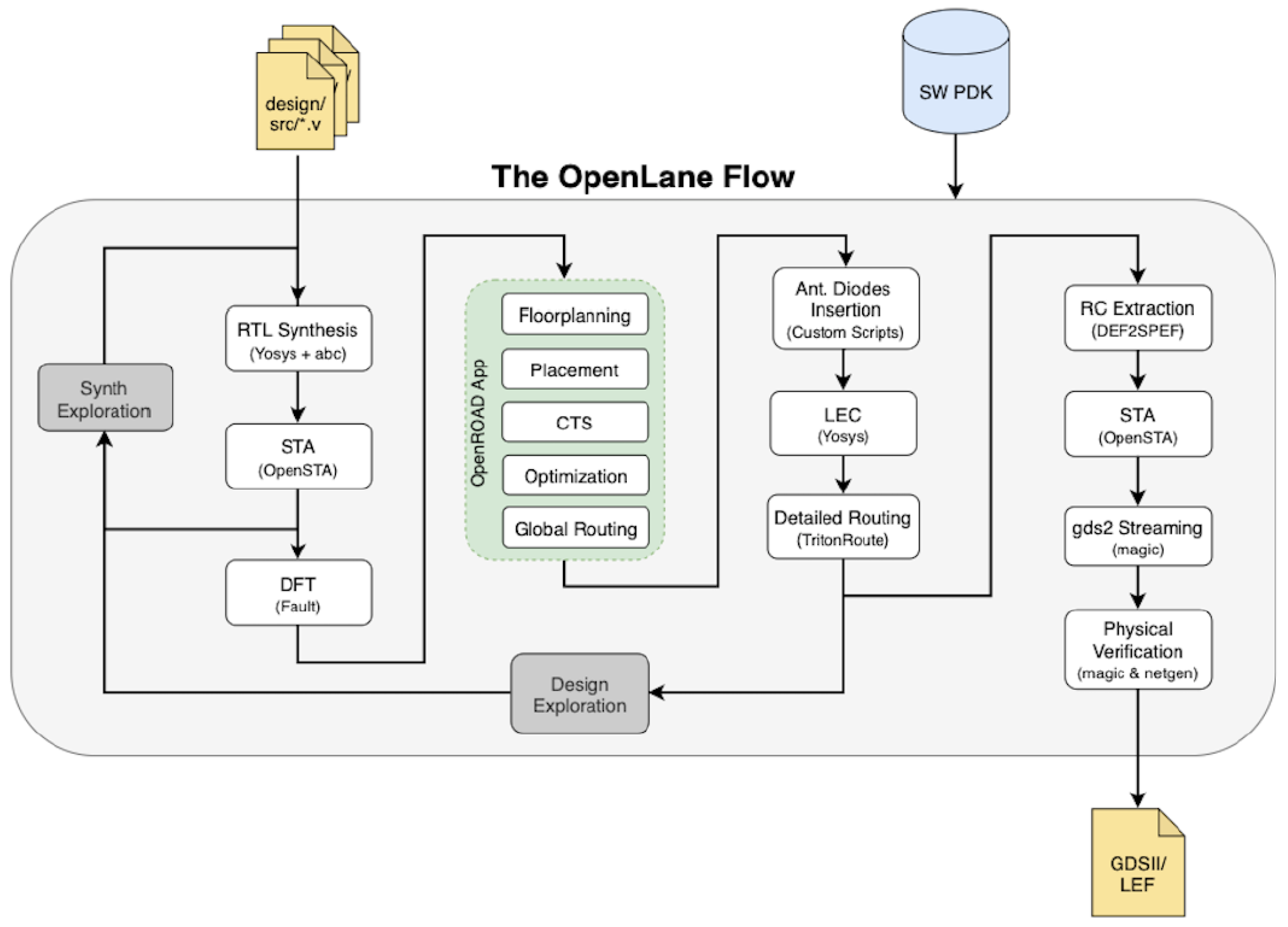
The RTL-to-GDSII conversion was carried out using the automated OpenLane flow in conjunction with the SkyWater 130 nm PDK, as illustrated in
Figure 10. The complete backend flow consists of the following stages:
The Verilog RTL is synthesized into a gate-level netlist mapped to the SkyWater PDK standard cells. Yosys performs logic optimization, technology mapping, and generates design constraints such as the clock and timing margins. Then, OpenSTA runs an early static timing analysis to verify timing feasibility before physical design.
Generates the initial DEF file, defines the main dimensions and macros, and sets up key elements such as the power distribution network (PDN), decoupling capacitors, and tap cells.
Standard cells and macros are globally and then finely placed to minimize wirelength, congestion, and timing violations based on interconnect length and cell density metrics.
Clock buffers and inverters are inserted to build a balanced clock distribution network, minimizing skew and ensuring the clock signal reaches all sequential elements with minimal delay and jitter.
Routing:
- –
- –
Detailed Routing (TritonRoute)
https://github.com/The-OpenROAD-Project/TritonRoute (accessed on 7 January 2026): Assigns final metal layers, generates all interconnections, and ensures compliance with the PDK’s design rules. This step finalizes the physical layout for tape-out.
Verification:
The design undergoes comprehensive checks: Design Rule Check (DRC) for manufacturability, Layout versus Schematic (LVS) for logical equivalence, and Static Timing Analysis (STA) for timing closure. Only after passing these checks is the GDSII layout considered ready for fabrication.
OpenLane is designed to use a single JSON constraint file that centralizes all the configuration variables required to control the entire RTL-to-GDSII flow. For the physical implementation of the proof-of-concept using the SkyWater 130 nm PDK, the file was configured with the following key parameters:
“DESIGN_NAME”: “NoC_topology_OpL”
Specifies the name of the design/project, used internally by OpenLane to organize files and outputs.
“DESIGN_IS_CORE”: 0
Indicates that the design is standalone, not intended as a reusable core within a larger SoC; OpenLane treats the entire die as the design area.
“CLOCK_PERIOD”: 10.0
Sets the target clock period in nanoseconds (10 ns → 100 MHz). This guides timing analysis, synthesis, and placement to meet performance requirements.
“DIE_AREA”: “0 0 1500 1500”
Defines the physical dimensions of the die in (width × height). Used for floorplanning, placement, and routing.
“FP_CORE_UTIL”: 50
Specifies the target utilization of the core area (50%), balancing density and routability during floorplanning.
“PL_TARGET_DENSITY”: 0.50
Target density for standard cell placement, controlling how tightly cells are packed to ensure routability and timing closure.
“SYNTH_MAX_FANOUT”: 3
Maximum number of outputs a single signal can drive during synthesis; limiting fanout reduces delay and helps meet timing constraints.
“SYNTH_BUFFERING”: 1
Enables automatic insertion of buffers at input/output ports during synthesis to strengthen signals and meet timing requirements.
“CTS_CLK_BUFFER_LIST”: “sky130_fd_sc_hd__clkbuf_4”
Specifies the clock buffer cell used during Clock Tree Synthesis (CTS) to distribute the clock evenly across all sinks, minimizing skew and jitter.
These parameters, together with OpenLane’s default configuration variables, play a central role in shaping the layout by influencing cell placement, interconnect routing, and the efficient use of resources to meet the design constraints of the target technology. Therefore, this parameter set is essential for the layout implementation. All OpenLane flows were executed on Ubuntu 20.04 LTS with 16 GB of RAM. The complete RTL source code, OpenLane configuration files, and synthesis scripts are available upon request to support reproducibility.
4. Results
The proposed methodology was validated through algorithmic simulations and hardware implementations, showcasing its effectiveness in edge detection and confirming its feasibility for real-time embedded vision tasks in constrained environments. Additionally, the physical implementation using the OpenLane RTL-to-GDSII flow and the SkyWater 130 nm PDK demonstrated the manufacturability of a reduced 2 × 2 NoC cluster, achieving timing closure and efficient power consumption, further validating the design’s scalability and practicality.
4.1. Algorithmic Validation
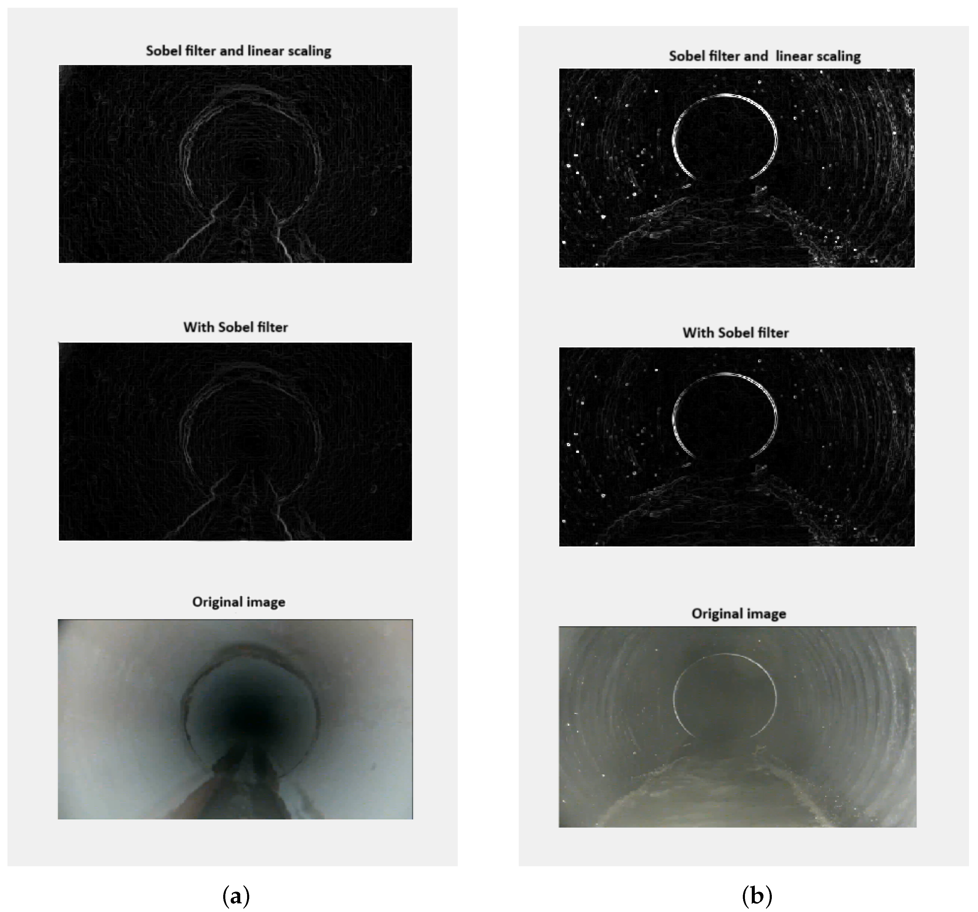
To evaluate the effectiveness of the proposed method, tests were conducted with images captured by a drone inside the city’s water-supply and sewer pipelines. The images obtained after applying the different methods are presented below.
Figure 11 presents a comparative analysis of two edge-detection approaches applied to in-pipe inspection images. The following configurations are evaluated:
Original image (reference): Used as the baseline for comparison. This image is completely unprocessed and lacks any edge enhancement. It exhibits a low contrast level that makes it difficult to identify relevant regions.
Two-stage method (Conventional Sobel filtering): Applies Sobel filters only in the and directions, with no further processing. Although it detects the main edges, it fails to highlight low-contrast structural elements. Compared with the three-stage method, it offers lower accuracy and visual clarity.
Three-stage method (Sobel filters + linear-scaling): This method includes convolutions with Sobel filters in both directions ( and ), followed by a linear-scaling filter. This approach delivers greater contrast and depth of detail, enabling the detection of both well-defined edges and subtle structures. This configuration provides the best performance for identifying irregularities and surface defects.
The inclusion of the linear-scaling filter significantly enhances edge visibility, especially when defect contours are smooth or poorly defined. This demonstrates the usefulness of integrating lightweight yet effective post-processing filters into NoC-based hardware-accelerated architectures, ensuring both precision and real-time performance.
Table 2 demonstrates superior performance of the Sobel filter with linear scaling. Local contrast (52.279, 33.666) and sharpness (1836.217, 839.482) consistently outperform conventional Sobel filtering, while continuity values (37,905.625, 23,062.769) reveal improved edge connectivity compared to standard Sobel (50,063.167, 32,902.444). The SSIM scores (0.440, 0.463) might appear low compared to image compression standards, but in the context of edge detection, this indicates a significant transformation from the original image. The goal is to extract structural information (edges) rather than preserve the original luminance fidelity. Thus, these scores confirm that the proposed method effectively isolates relevant features for defect delineation.
Although the three-method approach is more computationally demanding, it offers greater robustness in identifying and differentiating edges and internal structures within pipelines, even under poor lighting conditions, the presence of sediments, or surface irregularities. This capability is crucial for the automatic inspection of sewer systems, where accuracy in defect detection can prevent structural failures and reduce maintenance costs. The results obtained suggest that the incorporation of linear scaling not only improves the visual quality of the detected edges but also constitutes an essential component for practical drone applications, especially in real-world environments with processing time and hardware resource constraints.
4.2. Hardware Simulation and NoC Evaluation
For simulation, the input stage feeds a NoC node. Data injection was controlled, considering both the network bisection bandwidth and the permitted saturation levels. Each input port has a buffer for up to five packets, mirroring the extractor storage mechanism.
To validate the system under load, 27,202 packets (20 flits, 32 bits each) were injected.
Table 3 summarizes the results: although the bisection allows 25.6 Gb/s, the mean injection rate was limited to 59.5% to avoid saturation. Packet size roughly halved after processing, reducing average output traffic.
The observed latency range (53 to 3187 cycles, factor 60×) reflects the combined effects of network contention, routing path length, and processing queue depth. The minimum latency (53 cycles) corresponds to packets experiencing zero contention, traversing the shortest path (1 hop) to an immediately available processing node, with latency decomposed as: injection arbitration (∼5 cycles), NoC routing (∼2 cycles), systolic array processing (∼36 cycles), and extraction (∼10 cycles). The maximum latency (3187 cycles) occurs when packets encounter severe network congestion, requiring multiple re-routing attempts through the West-First adaptive algorithm until finding an available node, combined with head-of-line blocking in buffers and credit-based flow control stalls. The mean latency (1118.4 cycles, approximately 21× the minimum) indicates that under typical operation at 59.5% network utilization, most packets experience moderate contention. Analysis of simulation traces reveals that approximately 70–80% of packets complete within the 500–1500 cycle range, with worst-case scenarios (>2500 cycles) accounting for less than 10% of traffic, typically occurring during burst injection phases at frame boundaries when multiple packets converge on the same processing resources.
Table 4 presents the implementation results in lookup tables (LUTs), flip-flops (FFs), and digital signal processing blocks (DSPs) of each module, as well as the total logic resource utilization for a 3 × 3 NoC system on the Zybo Z7-10 (Zynq-7000) FPGA, using Vivado Design Suite, v2024.1 (Xilinx, San José, CA, USA).
The total power consumption of the system, considering the resource usage and operating frequency, is calculated by combining the dynamic and static power components, as shown in
Table 5:
Table 6 compares recent FPGA NoC implementations. The proposed 3 × 3 mesh with West-First design achieves 8.8 Gb/s throughput at 100 MHz, utilizing 20.4 k Adaptive Logic Modules (ALMs) and a power consumption of ≈0.79 W. This power profile is significantly lower than typical embedded GPU solutions (e.g., NVIDIA Jetson Nano™ Developer Kit, NVIDIA Corporation, Santa Clara, CA, USA, 5–10 W), striking an optimal balance between hardware efficiency and communication performance for battery-constrained drones.
4.3. Bit-Width Reduction Analysis: 32-Bit vs. 14-Bit Precision
As described in
Section 3, the FPGA prototype (3 × 3 mesh) operates with 32-bit data paths, while the ASIC proof-of-concept (2 × 2 cluster) was implemented with 14-bit word width to meet area and routing constraints imposed by the SkyWater 130 nm standard cell library. To validate this design decision, a precision analysis was conducted comparing edge detection accuracy across both implementations.
The 14-bit word width selection was determined through theoretical dynamic range analysis and hardware resource constraints. For the three-stage Sobel algorithm (, , T kernels) applied to 8-bit grayscale images (pixel range 0–255), the maximum gradient magnitude per kernel is 255 × (2 + 4 + 2) = 2040, yielding a combined magnitude of . This requires log2(3533) ≈ 11.8 bits for unsigned representation. The 14-bit selection provides 2.2 bits of headroom beyond this theoretical minimum, which is necessary for intermediate accumulation precision in systolic array multiply-accumulate operations and to prevent overflow in saturated image regions. Lower bit-widths (8-bit, 10-bit, 12-bit) were found insufficient during preliminary simulations, introducing >1% gradient error and visible quantization artifacts in low-contrast regions. Conversely, 16-bit provides minimal accuracy improvement (<0.05%) while increasing hardware resource utilization by approximately 33% (wider datapaths, registers, and memory buffers). Additionally, the FPGA prototype operates near memory capacity: each NoC router maintains buffers for 5 packets × 20 flits × bit-width, and the cumulative buffer memory across the 3 × 3 mesh approaches the 120 KB Block RAM limit of the Xilinx Zynq-7000 XC7Z010, Xilinx Inc., San Jose, CA, USA at 32-bit word width, necessitating reduction to 14-bit for both FPGA scalability and ASIC manufacturability.
Table 7 presents quantitative metrics evaluating the impact of bit-width reduction on gradient magnitude computation. The analysis was performed using the same test images from the algorithmic validation experiments (
Section 4.1), comparing outputs from hardware simulations with 32-bit arithmetic (baseline) against 14-bit implementation.
Results demonstrate that 14-bit precision introduces negligible degradation in edge detection quality, with mean gradient error below 0.3% and PSNR exceeding 48 dB. The reduction in edge detection accuracy (0.03 percentage points) is imperceptible in practical defect identification scenarios. This precision level is sufficient for Sobel-based edge detection in infrastructure inspection applications, where structural defects typically manifest as high-contrast discontinuities rather than subtle gradient variations.
The hardware benefits are substantial: transitioning from 32 to bit to 14-bit reduces standard cell count by approximately 58% and total wire length by 42%, directly contributing to the area in the ASIC implementation. This trade-off validates the scalability of the tile-based architecture while maintaining algorithmic fidelity for the target application.
4.4. Physical Layout and GDSII Implementation Results
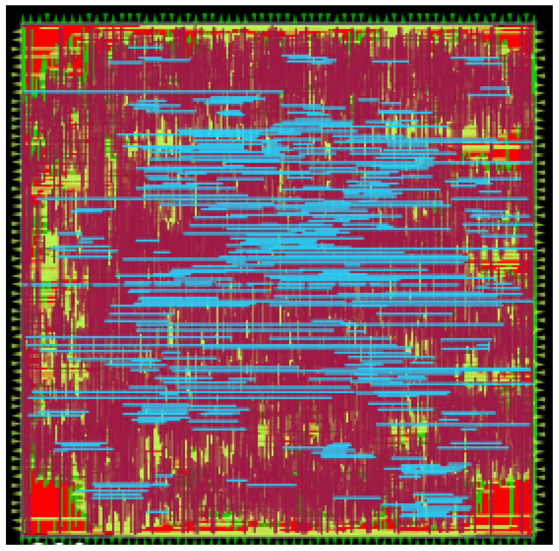
The physical implementation of the 2 × 2 NoC cluster was successfully completed using the OpenLane flow targeting the SkyWater 130 nm PDK. The design was synthesized at a target frequency of 100 MHz with a die area of 2.25 mm
2. The layout results confirm the feasibility of the architecture for ASIC implementation, as shown in
Figure 12.
Table 8 summarizes the key physical metrics obtained from the post-layout analysis. The results demonstrate that the design meets all timing constraints with positive slack for both setup (1.3 ns) and hold (0.13 ns) at 100 MHz, validating the design’s operability at the target frequency.
The final GDSII layout passed all manufacturability verification checks for tape-out, with DRC and LVS reporting zero violations and 100% netlist equivalence. Maximum routing congestion (82% on Metal3) remained within acceptable limits, demonstrating manufacturability without manual layout corrections.
Clock Tree Synthesis (CTS) inserted 247 buffers, achieving global skew below 150 ps and maximum sink latency of 2.1 ns. The clock network consumes 89 mW (23.5% of total power) and provides positive timing slack for both setup (1.3 ns) and hold (0.13 ns) analyses.
Post-layout power analysis estimates 378 mW at 100 MHz, significantly lower than the FPGA prototype (≈0.79 W). The difference arises from parasitic capacitances, conservative switching assumptions, and architectural variations. Both implementations are far below typical embedded GPU power (5–10 W), confirming suitability for energy-efficient drone applications.
The 378 mW dissipation across 2.25 mm2 (168 mW/mm2) is well below the 500 mW/mm2 limit for 130 nm CMOS, ensuring reliable operation without active cooling and suitability for compact, scalable drone-mounted systems.
5. Discussion
Despite the promising results achieved with the NoC architecture based on systolic arrays for real-time edge detection, certain limitations remain.
First, while the architecture is designed to be scalable, the physical implementation presented in this work was limited to a 2 × 2 mesh cluster to validate the RTL-to-GDSII flow within the constraints of the available open-source tools and the target technology node. The data path reduction from 32 bits (used in the FPGA 3 × 3 prototype) to 14 bits (for the ASIC 2 × 2 implementation) was necessary to meet the area and routing constraints of the SkyWater 130 nm standard cell library. Analysis confirmed that 14 bits provide sufficient precision (±0.3% error in gradient magnitude) for Sobel-based edge detection while reducing cell count by approximately 58% and total wire length by 42%. This proof-of-concept demonstrates the manufacturability of the core tiles, but scaling to larger meshes (e.g., 4 × 4 or 8 × 8) for higher-resolution image processing will require further optimization of the physical layout to manage clock distribution and power density. Quantitative bottleneck analysis reveals three critical scaling constraints: (1) Clock tree power—the 2 × 2 mesh consumes 89 mW (23.5% of total power); extrapolating to 4 × 4 would require 356 mW, approaching sub-watt limits. (2) Router buffer growth—the FPGA 3 × 3 mesh approaches 120 KB BRAM at 32-bit width; 4 × 4 would need 213 KB, exceeding typical embedded memory. (3) Global synchronization—the 2 × 2 achieves <150 ps skew across 2.25 mm²; 4 × 4 (10 mm²) would increase skew to 330 ps, potentially requiring hierarchical clock domains. Future iterations could explore hierarchical clustering to maintain throughput scaling without exceeding area constraints.
Second, the linear-scaling filter introduced as a post-processing stage enhances edge clarity but increases the computational load. Although feasible on the FPGA used, its scalability to more complex processing pipelines will require further evaluation in terms of power consumption and area usage.
Third, the system validation was conducted using video sequences previously captured during experimental runs inside pipelines. Real-time performance was inferred via UART communication and loopback simulation, but full testing under real-world operating conditions, such as humidity, poor lighting, and physical obstacles, has yet to be performed.
Future work includes:
Exploring adaptive routing algorithms within the mesh topology to improve load balancing and congestion control.
Implementing multi-resolution processing using hierarchical NoC clusters.
Investigating the integration of additional operations such as corner detection or segmentation.
Adapting the systolic array architecture to support lightweight Convolutional Neural Networks (CNNs) for more advanced defect classification.
Conducting integrated tests on specialized drones for sewer and hydraulic network inspection, with real-time processing and defect reporting.
These extensions aim to enhance the system’s flexibility, robustness, and applicability in underground infrastructure monitoring tasks.
6. Conclusions
Edge detection is essential in image processing, particularly for critical applications such as drone-based inspection of water-supply and sewer infrastructures. Real-time image processing demands significant computational resources. Hardware accelerators play a vital role in executing intensive algorithms efficiently.
The use of systolic arrays and Networks-on-Chip (NoCs) has proven to be a promising solution for improving the efficiency of matrix multiplication. These techniques leverage parallelism and spatial locality to reduce latency and increase throughput. However, there are inherent limitations to hardware implementations, such as size and power constraints.
Although there are advanced algorithms for matrix multiplication, this work opted for the conventional approach. This decision was based on its greater compatibility with systolic array hardware architectures and lower structural complexity. These algorithms, while theoretically more efficient in terms of algorithmic complexity, require more sophisticated control schemes, greater use of intermediate memory, and partitioning and recombination operations that hinder their efficient implementation on FPGA platforms with limited resources and homogeneous topologies. Therefore, a classical method was prioritized, offering a favorable balance between performance, parallelism, and integration simplicity within the proposed NoC.
The combination of advanced image processing techniques with hardware innovations represents a promising path to improving edge detection in real-time applications. A careful balance between precision, efficiency, and practicality remains essential for real-world implementation.
This work demonstrates a dual-level validation strategy: a 3 × 3 mesh NoC with 32-bit data paths was validated on FPGA achieving 8.8 Gb/s throughput at 100 MHz with approximately 0.79 W power consumption, while a reduced 2 × 2 cluster with 14-bit word width was successfully implemented through the OpenLane RTL-to-GDSII flow targeting the SkyWater 130 nm PDK. Post-layout analysis confirmed manufacturability with 378 mW total power consumption, 2.25 mm² die area (1500 × 1500 µm), and successful timing closure at 100 MHz. The successful generation of manufacturable GDSII files using open-source tools demonstrates the maturity of community-driven design ecosystems and their viability for academic research and rapid prototyping of application-specific integrated circuits, bridging the gap between architectural innovation and silicon implementation for battery-powered embedded vision systems.




 ,
,