1. Introduction
Modern developments in optoelectronic devices for the visible and near-infrared ranges, particularly in medical and industrial equipment, need to solve the problem of electromagnetic compatibility (EMC). These devices must operate efficiently in the optical spectral range, despite the effects of electromagnetic interference in the microwave range. The sources of such interference can be lightning, powerful radars, gyrotrons, klystrons, wireless communication devices, etc. The article [
1] presented an overview of electromagnetic interference (EMI) threats, discussed an approach to assessing the consequences they produce, and proposed options for mitigating them. Image disruption in a digital CCD camera caused by a controlled electromagnetic interference was studied in [
2]. The emergence of image abnormalities in complementary metal oxide semiconductor (CMOS) image sensors when exposed to high-power electromagnetic radiation was experimentally studied in [
3]. A very recent article [
4] examines the current state of research on attack methods targeting camera systems, providing a comprehensive review of various electromagnetic attack methods and their implications.
In this regard, specialized shielding filters are being actively developed to suppress unwanted electromagnetic interference (EMI) from passing into optoelectronic devices having simultaneously high transparency in the optical range [
5,
6]. Transparent conductive oxides [
7], such as indium tin oxide (ITO) [
5,
8,
9,
10,
11], indium zinc oxide (IZO) [
6,
12,
13], zinc-doped tin oxide (ZTO) [
12,
14], aluminum-doped zinc oxide (AZO), and fluorine-doped zinc oxide (FZO) [
15].
The most studied and widely used oxide semiconductor is ITO. Its thin films are characterized by ultra-low resistivity (which provides high microwave shielding effectiveness) and high transmittance in the visible spectral region. The optical properties of ITO films in the visible spectral region have been studied in sufficient detail (see [
7,
16] and references therein). According to experimental studies, ITO films with a DC sheet resistivity of
= 3.5–22 Ohm/sq provide an average optical transmittance of 0.80–0.84 (in the visible wavelength region from 0.4 to 0.8 µm) [
16]. At the same time, the results of studies of the interaction of microwave radiation with ITO-based shielding filters are quite fragmentary. According to [
17], in the frequency range of 8.5–12 GHz, the maximum value of the shielding effectiveness, 26.8 dB, was obtained using ITO film with a sheet resistivity of 14.8 Ohm/sq, with a transmission value in the visible range of ~0.7. The authors of [
18] experimentally observed a decrease in the shielding effectiveness from 20 to 16 dB with an increase in the radiation frequency from 2 to 12 GHz for an ITO film with a sheet resistivity of ~20 Ohm/sq, with an average transparency of ~0.84 in the wavelength range of 0.38–0.77; however, the physical nature of the observed dependencies were not discussed in their work. In [
19], an ITO film with a lower DC sheet resistivity (
~4 Ohm/sq) deposited on K108 glass was studied. The experiment demonstrated good transparency of the structure in the visible range (~0.8) and an increase in the shielding effectiveness from 26 to 34 dB with an increase in the radiation frequency from 12 to 24 GHz. The paper [
19] noted that the relatively high efficiency of microwave shielding in the ITO film/K108 glass structures is due to the high reflectivity of the ITO film, while the absorption losses are negligibly small. However, the cited paper also did not provide a theoretical analysis of the spectral dependence of the shielding effectiveness.
The paper [
20] aimed to develop ITO-coated PET-based microwave metamaterial
absorbers. In the 4–16 GHz range, a peak absorptivity of 0.986 was observed (apparently, the shielding effectiveness was ~20 dB). Li et al. developed a high-performance microwave absorber, which is a glass slab sandwiched between two ITO films with different sheet resistances [
21]. They achieved a shielding effectiveness of 24.3 dB (absorptivity of 0.995) in the 13–16 GHz range with a visible transmittance of 0.89.
Feng et al. developed and experimentally investigated EMI shielding filters with excellent parameters [
22]. They applied a multilayer ITO/Ag/ITO film to the polycarbonate substrate, which provided a shielding effectiveness of 36.5 dB in the 8–26 GHz range with a light transmittance of 0.875 at a wavelength of 550 nm. Furthermore, they designed a symmetrical structure with multilayer ITO/Ag/ITO films applied to both sides of the polycarbonate substrate, which resulted in a significant increase in shielding effectiveness to 67.5 dB, while maintaining a rather high light transmittance of 0.857. The article does not provide a theoretical analysis of the microwave transmission spectra of the structures studied.
In the present paper, we perform a comprehensive study aimed at improving EMI shielding windows for optoelectronic systems. The object of the study is ITO film-based shielding filters, which use borosilicate glass K108 as a substrate. Borosilicate glass is a standard material for protective windows in optoelectronic devices due to the following properties: high structural perfection of the glass (enabling high-quality images with large diameters and thicknesses of the protective glass); low absorption coefficient and low refractive index in the visible range (ensuring high transparency); relatively high hardness and chemical resistance, as well as a low coefficient of thermal expansion (which is important for outdoor applications of optoelectronic devices); commercial availability of glass substrates of various thicknesses and lateral dimensions. Two grades of borosilicate crown glass are commonly used to fabricate optical windows and lenses: BK7 (SCHOTT) and its radiation-resistant analog, K108 (LZOS). For this study, we found it convenient to use K108 glass as a substrate material, as we had previously obtained experimental data on the complex refractive index of this glass over a wide spectral range, including optical, terahertz, and microwave frequencies [
23]. This allowed us to numerically model the transmission and reflection spectra of the ITO film/K108 glass structures under study.
The interaction of the shielding filters with microwave radiation in the frequency range of 2–23 GHz was experimentally studied, which significantly expands the operating range towards lower frequencies. Furthermore, experimental studies were conducted on ITO films with rather low values of DC sheet resistivity—down to 2.3 Ohm/sq. As far as we know, there are no published data on the precise transmittance and reflectivity spectra of the ITO film-based shielding filters in such a wide area of microwave spectral range with such a small value of the ITO film sheet resistivity.
Theoretical modeling of microwave transmission and reflection for the ITO-based shielding filters has been performed using the transfer matrix method. The cases of normal and oblique incidence of microwave radiation are considered. The model spectra adequately describe the experimental results. It was shown that for a given substrate thickness, the spectral characteristics of the filters depend on a single parameter—the DC sheet resistivity of the ITO film. The dependence of the filter’s spectral characteristics on the glass substrate thickness was considered. The possibility of improving the spectral characteristics of filters by using substrates with a lower static dielectric constant was discussed.
For the first time, a method has been developed for predicting the microwave shielding efficiency of ITO film/K108 glass structures based on measurements of the structure’s transmission in the terahertz range, which are carried out using less complex measuring equipment. This method provides an error of less than 0.7 dB.
Finally, studies have been conducted aimed at increasing the transparency of the ITO-based microwave shielding filters in the optical spectral range. This task was solved by using antireflective coatings applied to both surfaces of the structure.
2. Transmittance and Reflectivity Spectra of the Shielding Filters in the Microwave Range: Theoretical Modeling
In this paper, we examine shielding filters, which are a thin ITO film on glass. Experiments with microwave radiation were carried out at frequencies
from 3 to 23 GHz. At such low frequencies, the dielectric constant of a conductive ITO film can be described in the framework of the Drude model, where the square of the complex refractive index of the film,
, turns out to be purely imaginary and can be expressed in terms of the DC sheet resistivity of the film
and the film thickness
as follows [
16]:
which results in
Here, we use the Gaussian system of units in all analytic expressions. The conditions for the applicability of relations (1) and (2) to ITO films in the specified frequency range are the inequalities
≪ 32,000 cm
2/(Vs) and
=
≪ 1.6 Ohm·cm, where
and
are, respectively, the electron mobility and DC volume resistivity of the film. With respect to conducting ITO films of submicron thickness obtained by cathode sputtering of indium and tin oxides in a magnetron discharge plasma, these conditions are obviously fulfilled (see [
16]).
Prior to discussing the interaction of microwave radiation with ITO film/K108 glass structures, it is advisable to consider the microwave performance of a free-standing ITO film. Film transmission and reflection modeling can be performed using the transfer matrix
M:
where
and
are transfer matrices for the interfaces vacuum/ITO film and ITO film/vacuum, respectively:
and the propagation matrix for the ITO film is indicated by
:
Transmittance
, reflectivity
, and absorptivity
of the free-standing ITO film can be found using the following equations (for details, see [
16]):
Relations (1)–(6) show that in this case the coefficients
,
, and
are uniquely determined by the two quantities:
and (
). With a fixed value of DC sheet resistivity, the refractive index
and extinction coefficient
are inversely proportional to
, while the electromagnetic wave phase shift
after passing the film is directly proportional to
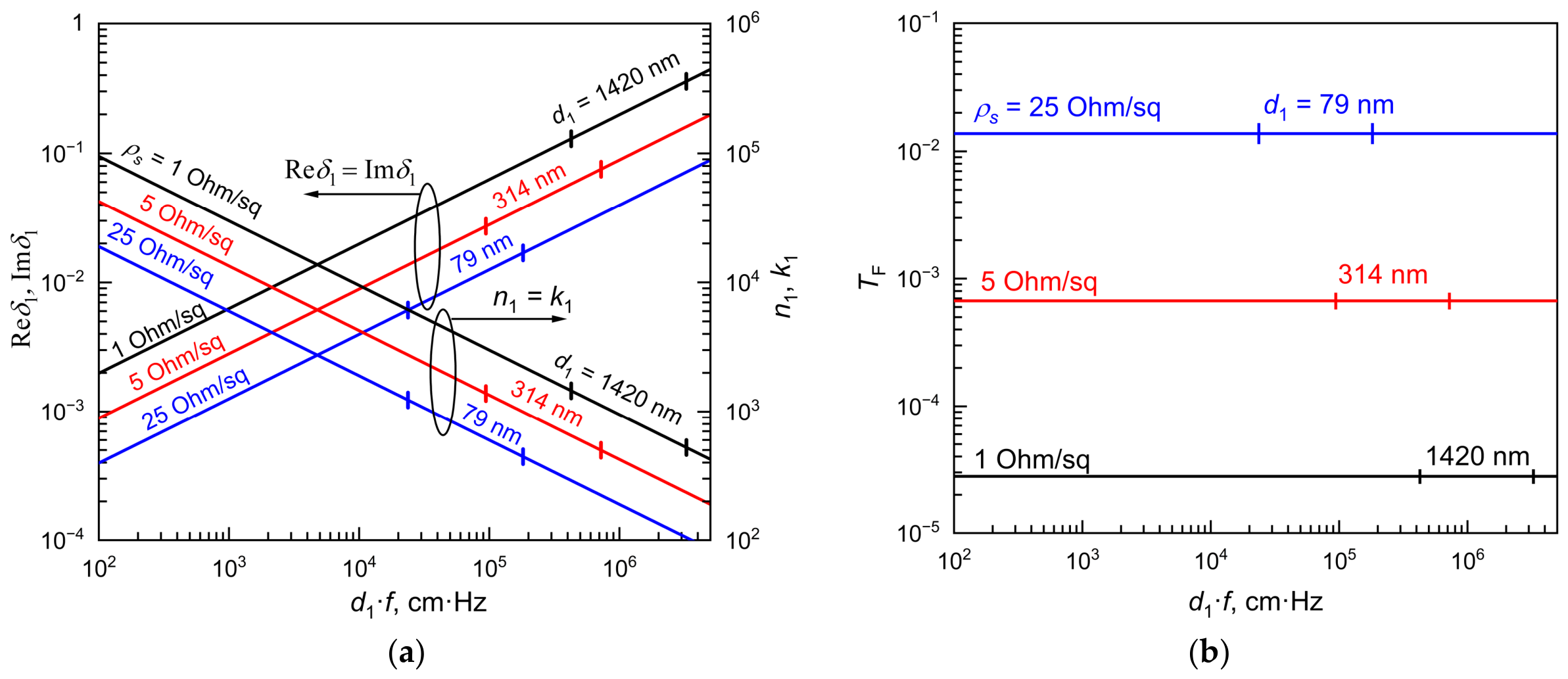
. The transmittance simulation results for the free-standing ITO films turn out to be rather unexpected: when the value (
) changes by several orders of magnitude, the relative transmittance change becomes very small (for a fixed value of DC sheet resistivity), see
Figure 1. For example, when
= 5 Ohm/sq, a decrease in (
) by four orders of magnitude is accompanied by an increase in
n1 and
k1 by two orders of magnitude and a decrease in Re
and Im
by two orders of magnitude, while transmittance
varies negligibly: from 3.4348 × 10
−4 to 3.4375 × 10
−4 (the relative transmittance change is only ~0.0008).
In the limit
corresponding to thin films and low frequencies, the Formulas (1)–(6) result in
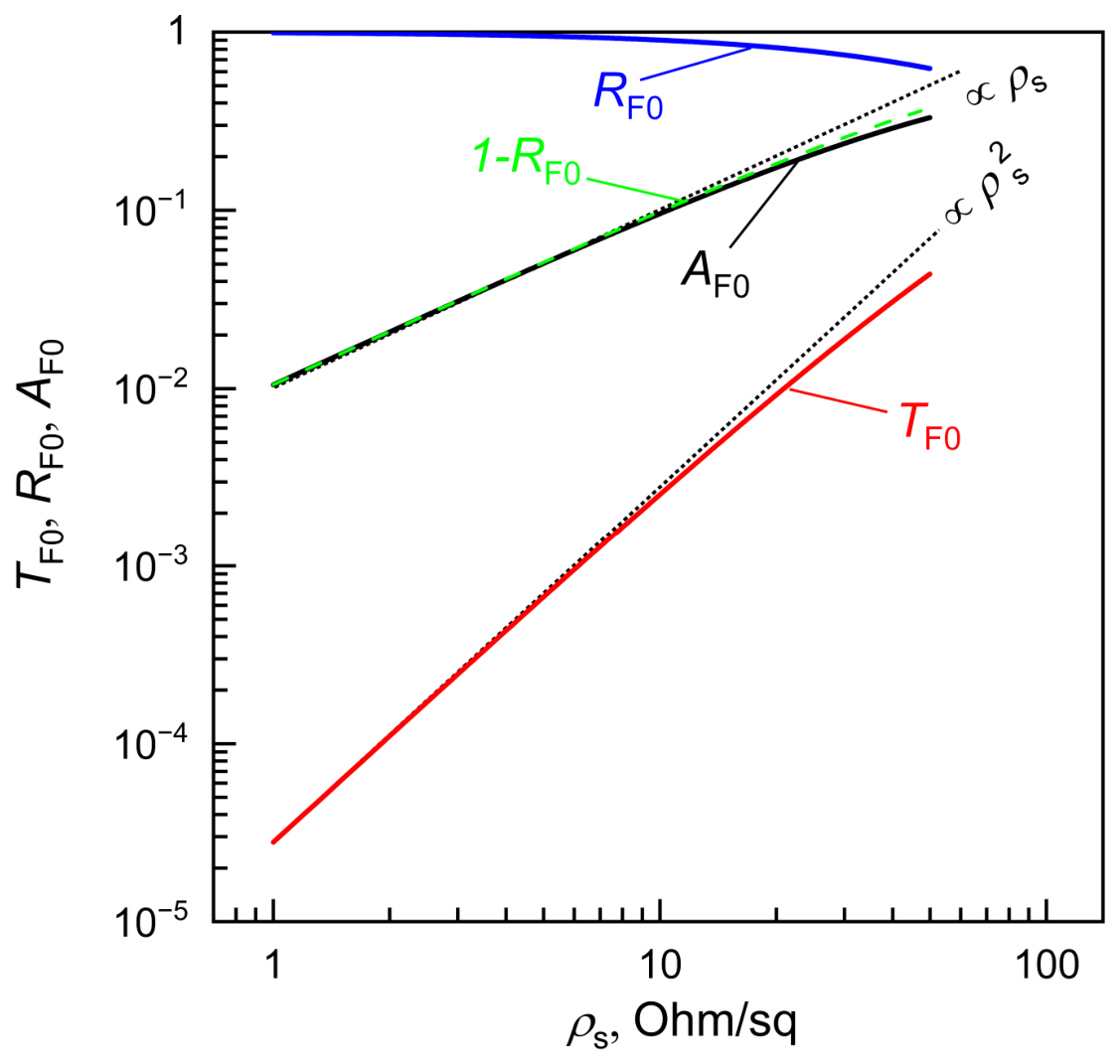
Figure 2 shows the calculated dependences of these limit values on the DC sheet resistivity in the range from 1 to 50 Ohm/sq. As can be seen from the figure, the transmittance
decreases rapidly with decreasing the DC sheet resistivity, while the dependence
) asymptotically tends to the quadratic function
. In the range
= 1…10 Ohm/sq the transmittance has a very small value: ~10
−5…10
−3. This is largely due to the high reflectivity
, namely,
→1 at
→0. The dashed line in
Figure 2 shows the fraction of non-reflected radiation (
. As can be seen from the figure, it is very close to absorptivity:
As the DC sheet resistivity decreases, both of these values asymptotically approach the linear function const ×
and, as a result, the fraction of transmitted radiation
becomes smaller and smaller, decreasing according to the quadratic law at
≪
in the Gaussian system of units, or at
≪ 188 Ohm/sq.
To build the spectral dependence of the transmission for a free-standing ITO film at a given DC sheet resistivity of the film
, the film thickness
should be set. As a first approximation, we can use experimental data on the
dependence obtained in [
16] for ITO films produced by the method of cathode sputtering of an indium and tin oxide target in magnetron discharge plasma. According to the results of this work, ITO films with
= 1, 5, and 25 Ohm/sq have a thickness
= 1420, 314, and 79 nm, respectively. The spectra
calculated at the specified values of
and
within the frequency range
≤ 23 GHz are represented in
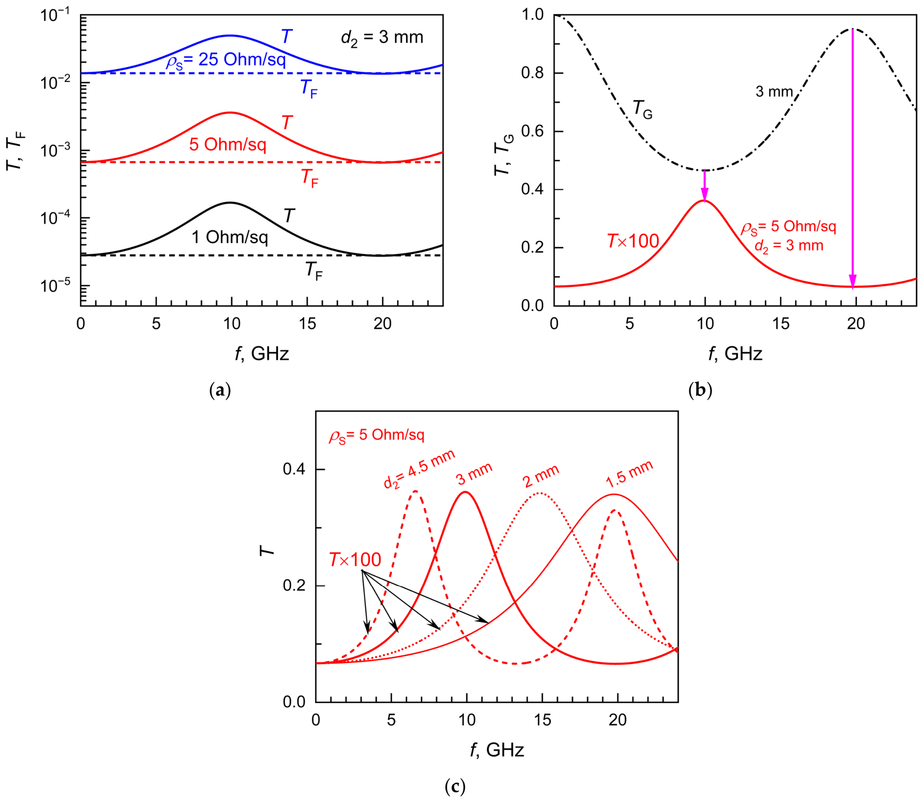
Figure 3a by dashed lines. Note that for a given DC sheet resistivity, the function
is monotonically decreasing, but even at the high-frequency boundary of our experiments (
= 23 GHz), the relative decrease in the transmittance in comparison to the transmittance limit
does not exceed 0.001 (for
1 Ohm/sq). Such a small change in
Figure 3a is not noticeable, being less than the width of the curve
. In other words, for transmission of the free-standing ITO film, the approximation
≈
is very good over the entire frequency range under study. Similarly, in
Figure 1b, no noticeable change in the values of the
function is observed for a film with a given DC sheet resistivity
within the experimentally studied range of
values. The value of
determines the ITO film thickness
. In the experiment, the minimum and maximum operating frequencies were 3 GHz and 23 GHz, respectively. In the figure, the boundaries of the experimentally examined range of the product
are marked with vertical strokes on each curve
.
In general, depending on the chosen ITO film manufacturing technology, the dependence of
) may vary.
Figure 4 shows the experimental dependences
from our work [
16] and from five other papers in which the ITO film was deposited on various substrates by magnetron sputtering with significantly different parameters (oxygen partial pressure, substrate temperature, and deposition rate). As can be seen from the figure, varying the technological parameters can result in a 2–4 times increase in the film thickness (compared to the value of
(
) from [
16]) for a given value of
. However, the calculation shows that even a 4-fold increase in thickness compared to
) from [
16] changes the transmittance
of free-standing ITO film negligibly: the relative change does not exceed 0.01. In
Figure 1b and
Figure 3a, such a change is less than the line width and not noticeable. Thus, using data on
(
) from [
16] is a very good approximation for modeling the microwave transmission of ITO films with DC sheet resistivity of 1 … 25 Ohm/sq—regardless of the film production technology.
Let us consider now the interaction of microwave radiation with an ITO film/K108 glass shielding filter. Earlier in [
16], the modeling of the transmission and reflection spectra of ITO film/K108 glass structures
in the optical range was considered, where radiation interference in the thick glass substrate was suppressed by the spectrometer resolution. For this, a modified transfer matrix method was used, in which the substrate was considered as an “incoherent layer” randomly changing the phase of the electromagnetic wave.
In the microwave range, on the contrary, interference in the glass substrate is well observed, and the usual transfer matrix method can be used to calculate the transmittance
T and reflectivity
R of the structures:
where
and
denote propagation matrices for ITO film (thickness
) and K108 glass (thickness
), respectively, and
,
, and
denote interface transfer matrices for vacuum/ITO film, ITO film/K108 glass, and K108 glass/vacuum interfaces, respectively (for details, see [
16]).
To numerically simulate the transmission and reflection spectra of ITO film/K108 glass shielding filters in the microwave spectral range (
< 24 GHz), Formula (1) for the complex refractive index of ITO film
was used, as well as experimental data on the complex refractive index and absorption coefficient of glass K108:
and
, where
and
are expressed in GHz and cm
−1, respectively [
23].
The simulation results for the transmittance spectra at a fixed glass thickness (
= 3 mm) but with different DC sheet resistivities of the film
are represented by solid lines in
Figure 3a. As for the case of free-standing films, the data on
) were taken from [
16].
Figure 3a demonstrates that the microwave transmittance of the ITO film/K108 glass structure varies greatly with the frequency of radiation. Obviously, this dependence is due to the interference of radiation in a thick glass substrate. Indeed, the minima of the transmittance curve of ITO film/K108 glass structure coincide in spectral positions with the maxima of the transmittance spectrum for a glass substrate without a film. Let us explain the reason for this inversion.
Interference oscillations in the microwave transmittance spectrum for a glass substrate without a film can be described by the Airy formula [
23]:
where
is the phase shift during the two-fold passage of radiation through a glass substrate,
is the intensity reflection coefficient for the glass K108/vacuum interface. The simulated microwave transmittance spectrum for bare K108 glass with a thickness of
= 3 mm is shown in
Figure 3b by a dashed line marked with label
. The spectral position of the
N-th interference maximum for a glass substrate without a film is determined by the condition
, i.e.,
Since for the K108 glass at
≤ 23 GHz
= const = 2.520, the first-order interference maximum (
N = 1, δ = 2π) corresponds to the frequency
= 19.8 GHz (see
Figure 3b).
At the same frequency in the ITO film/K108 glass structure, a phase jump of
(due to the reflection of the radiation wave from the well-conducting ITO film at the glass/film interface) is added to the phase shift when the radiation passes twice through the glass thickness (equal to
). This phase jump is provided with the relations:
(see Equation (2) and data on
in
Figure 1a). As a result, at this frequency in a substrate with a conductive interface,
, and the resulting transmission of the ITO film/K108 glass structure reaches a minimum value (see
Figure 3b). Similarly, at a frequency
= 0, the transmittance spectrum of the ITO film/K108 glass structure demonstrates the interference minimum of zero order (
= 0,
=
). It is important to note that for a given value of DC sheet resistivity of the film, the minimum transmittance values of the ITO film/K108 glass structure coincide with the transmittance value of the free-standing ITO film (see
Figure 3a).
Similarly, the spectral position of the
N-th interference minimum for a glass substrate without a film is determined by the condition
and can be obtained from the relation:
The interference minimum of zero order (
N = 0,
) corresponds to the frequency
= 9.9 GHz. When a conductive ITO film is applied to one of the glass surfaces, a phase jump of
is added to the indicated phase shift due to the reflection of the radiation wave at the glass/film interface. As a result, at this frequency,
changes sign:
, and the resulting transmittance of the ITO film/K108 glass structure reaches a maximum value (see
Figure 3b), which is several times higher than the transmittance of the free-standing ITO film.
The ITO film/K108 glass structure provides the most effective suppression of microwave radiation in frequency regions close to transmittance minima. With a glass substrate thickness of = 3 mm, these are the ≤ 3 GHz and 17 GHz ≤ ≤ 23 GHz regions. The simulation results confirm that, from the point of view of microwave radiation suppression, it is more expedient to use ITO films with low DC sheet resistivity: with a decrease in from 5 to 1 Ohm/sq, the microwave transmission decreases from ~8 × 10⁻⁴ to ~3 × 10⁻⁵ (in the indicated spectral regions).
Varying the thickness of the glass substrate makes it possible to shift the area of effective microwave radiation suppression. According to the simulation results, varying the thickness of the K108 glass over the range 1.5–4.5 mm makes it possible to cover the entire microwave range from 0 to 23 GHz (see
Figure 3c).
Finally, we examined how the microwave transmittance of the ITO film/K108 glass structure changes as the radiation propagation direction deviates from the normal to the structure’s surface. An incident electromagnetic wave of arbitrary polarization can be represented as a superposition of waves with
s-polarization (when the electric field of the wave is perpendicular to the plane of incidence) and
p-polarization (when the electric field of the wave lies in the plane of incidence). The transmittance of the ITO film/K108 glass structure for
s-polarized and
p-polarized radiation was calculated using the transfer matrix method and the formulas from paper [
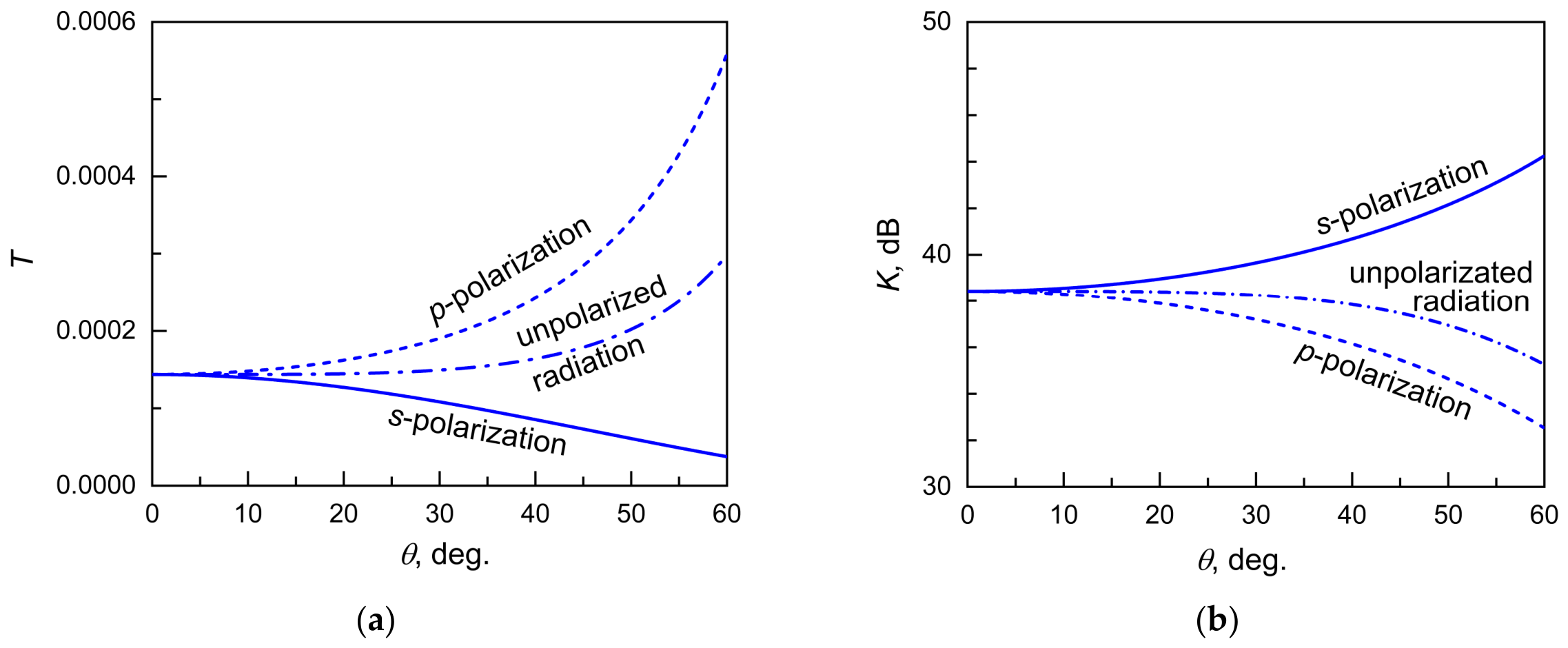
29]. An ITO film with a DC sheet resistivity of 2.3 Ohm/sq on 3 mm-thick K108 glass was considered. The calculations were performed for a frequency of
= 19.8 GHz, at which the minimum transmittance value is observed at normal radiation incidence (see
Figure 3a). Recall that the same low transmittance level is achieved at infinitely low frequencies (
. The calculation results are presented in
Figure 5a. As the angle of incidence
increases, transmittance
decreases monotonically for
s-polarized radiation, while it increases monotonically for
p-polarized radiation (in the range of angles considered). If the radiation is unpolarized, the transmittance can be found as half the sum of the transmittances for
s-polarized and
p-polarized radiation. Compared to
p-polarized radiation, the transmittance for unpolarized radiation increases significantly more slowly with increasing angle of incidence. It is more convenient to quantify the angular dependence of the microwave performance of shielding filters in terms of microwave shielding effectiveness, which is usually determined as
(dB) = 10 × lg(1/
). Calculations showed that for
s-polarization, with an increase in the incidence angle from 0° to 45°, microwave shielding effectiveness increases by 3 dB (from 38.4 dB to 41.4 dB), while for
p-polarization, it decreases by 3 dB (see
Figure 5b). The change in microwave shielding effectiveness for unpolarized radiation is only –0.9 dB, which can be considered insignificant.
3. Transmittance and Reflectivity Spectra of the Shielding Filters in the Microwave Range: Experiment and Discussion
To study the microwave performance of the shielding filters in the microwave range correctly, samples with a diameter exceeding the wavelength of the probing radiation are required. In this work, the operating frequency range extended from 3 to 23 GHz, which corresponds to wavelengths from 100 to 13 mm. For such studies, plane-parallel plates of K108 glass with a thickness of = 3 mm and a diameter of 200 mm were used.
For applying ITO films to a K108 glass plate, the method of cathode sputtering of an indium and tin oxides target (In2O3:SnO2 = 90:10) in magnetron discharge plasma was used. The target size was 820 × 80 mm. Sputtering was carried out in a reactive mode in an Ar + O2 gas mixture (300 and 15 cm3, respectively). The substrate was located parallel to the target and moved reciprocatingly along the target width at a speed of 10 mm/s. The substrate temperature was 300 °C. At a magnetron power of 5 kW, the film growth rate was 7.14 nm per pass. The resulting film thickness depended on the number of passes.
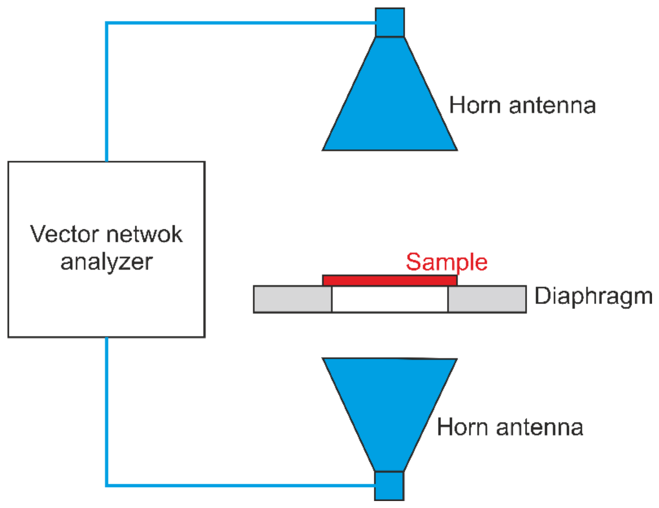
Measurements of the microwave transmittance and reflectivity spectra for the shielding filters were performed in free space using an anechoic chamber. A schematic diagram of the experimental setup is presented in
Figure 6. The vector network analyzer R&S ZVA40 was used as a microwave generator and detector. Ultra-wideband lens horn antennas were connected via coaxial cables to the generator output and detector input. The horn antennas were aligned vertically while the irradiated sample surface was oriented horizontally. The input aperture of 180 mm in diameter was provided by a circular metal diaphragm with broadband absorbing coatings. Sample transmittance and reflectivity were measured at normal incidence of microwave radiation. During reflectivity measurements, the microwave generator was simultaneously used as a detector. When conducting experiments, we followed the methodology described in the paper [
30]. All measurements were carried out with a spectral resolution of 0.01 GHz.
We also prepared witness samples with the same ITO films on round, plane-parallel plates of K108 glass with a thickness of 3.0 mm and a smaller diameter (50 mm). Firstly, these samples were used to determine the parameters of ITO films using non-contact methods developed earlier (see [
16]). Namely, the DC sheet resistivity of the ITO films,
, was determined from the transmittance spectra of the shielding filters measured using the terahertz time domain spectroscopy (THz TDS). Then, the ITO film thickness,
, was found from the transmittance and reflectivity spectra of the shielding filters in the optical range. In this paper, experimental studies were conducted for three ITO film/K108 glass structures with different thicknesses of conductive film
. The parameters of the structures studied are given in
Table 1.
Secondly, on the basis of witness samples, studies were conducted on the possibility of improving the performance of the shielding filters in the optical range by means of additional antireflective coatings (see
Section 4).
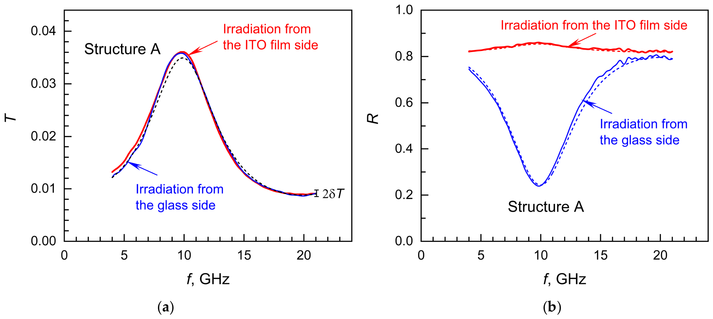
The results of the study of the microwave transmittance and reflectivity spectra for Structure A are presented in
Figure 7.
Figure 7.
Comparison of the experimental microwave transmittance and reflectivity spectra with simulated ones for Structure A under different conditions: (i) with normal incidence of microwave radiation at the ITO film surface and (ii) with incidence of the radiation at the glass surface. Experimental data are shown with solid lines, while the simulation results are shown with dashed lines. Structure parameters are listed in
Table 1. Simulated spectra are calculated at the best-fit value of
(see
Table 2). (
a) Transmittance spectra. (
b) Reflectivity spectra.
Figure 7.
Comparison of the experimental microwave transmittance and reflectivity spectra with simulated ones for Structure A under different conditions: (i) with normal incidence of microwave radiation at the ITO film surface and (ii) with incidence of the radiation at the glass surface. Experimental data are shown with solid lines, while the simulation results are shown with dashed lines. Structure parameters are listed in
Table 1. Simulated spectra are calculated at the best-fit value of
(see
Table 2). (
a) Transmittance spectra. (
b) Reflectivity spectra.
In the experiment, the transmission of ITO film/K108 glass structure was first measured under normal incidence of microwave radiation at the ITO film surface, and then under incidence of the radiation at the glass surface. The transfer matrix calculations show that the transmission spectra should be the same in both cases. The maximum transmittance at the frequency
= 9.9 GHz corresponds to the zero-order interference in the glass K108 with a thickness of
= 3 mm (see
Section 2). The slight difference between the two measured spectra is due to measurement errors (see
Figure 7a). For Structure A, the standard deviation of the experimental spectra from each other, averaged over the operating spectral range, is
= 6.3 × 10
−4. We took this value as the absolute error of the experiment. The minimum transmission of the structure
= 0.0088 ± 0.0006 was observed at a frequency
= 19.8 GHz, corresponding to the first-order interference minimum.
The model transmission spectrum of the ITO film/K108 glass structure can be calculated using the transfer matrix method (see
Section 2). Using the DC sheet resistivity of the ITO film as a fitting parameter, we adjusted the model spectrum for Structure A (dashed line on
Figure 7a) to match the experimental results (solid lines on
Figure 7a). The objective function
served as a measure of the deviation of the model spectrum from the experiment, where
is the number of experimental points;
and
are the experimental and simulated transmittance spectra, respectively, under irradiation from the ITO film side; and
and
are the experimental and simulated transmittance spectra, respectively, under irradiation from the glass side. As mentioned above,
. The best-fit value of the DC sheet resistivity of the ITO film for Structure A is
(19.9 ± 0.9) Ohm/sq. The absolute error for
was determined using the dependence of the objective function
on
near the minimum point, taking into account the accuracy of the experimental measurements of transmittance,
(for details, see [
16]). A convenient quantitative measure of the quality of the fit of the model curve to the experimental results is the coefficient of determination R
2. With the best-fit value of the fitting parameter
, the model microwave transmittance spectrum for Structure A is characterized by R
2 = 0.996, indicating good agreement between the modeling result and experiment.
The experimental reflectivity spectra for Structure A are presented in
Figure 7b by solid lines. The spectrum obtained when radiation falls on the structure from the side of the ITO film is radically different from the spectrum obtained when radiation falls from the opposite side (from the glass side). Firstly, these spectra are antiphase. Namely, at the frequency of
= 9.9 GHz, the first spectrum shows an interference maximum (of the zero order), while the second spectrum shows an interference minimum (of the zero order). On the contrary, at the frequency of
= 19.8 GHz, the first spectral curve reaches an interference minimum (of the first order), while the second one reaches an interference maximum (of the first order). Secondly, the contrast of the interference pattern (the ratio of the maximum reflectivity to the minimum one) for these two spectra differs significantly: when radiation falls on the structure from the side of the ITO film,
1.04, and when radiation falls from the side of the glass substrate,
3.3.
The reflectivity spectra of Structure A were modeled using the transfer matrix method
with the same parameters that were used above to model the transmittance spectra. The simulation results are shown in
Figure 7b with dashed lines. The patterns of reflectivity spectra revealed in the experiment are in satisfactory agreement with the simulation results. In particular, the coefficient of determination R
2 = 0.993 for the model reflectivity spectrum of Structure A under the incidence of the microwave radiation at the glass surface.
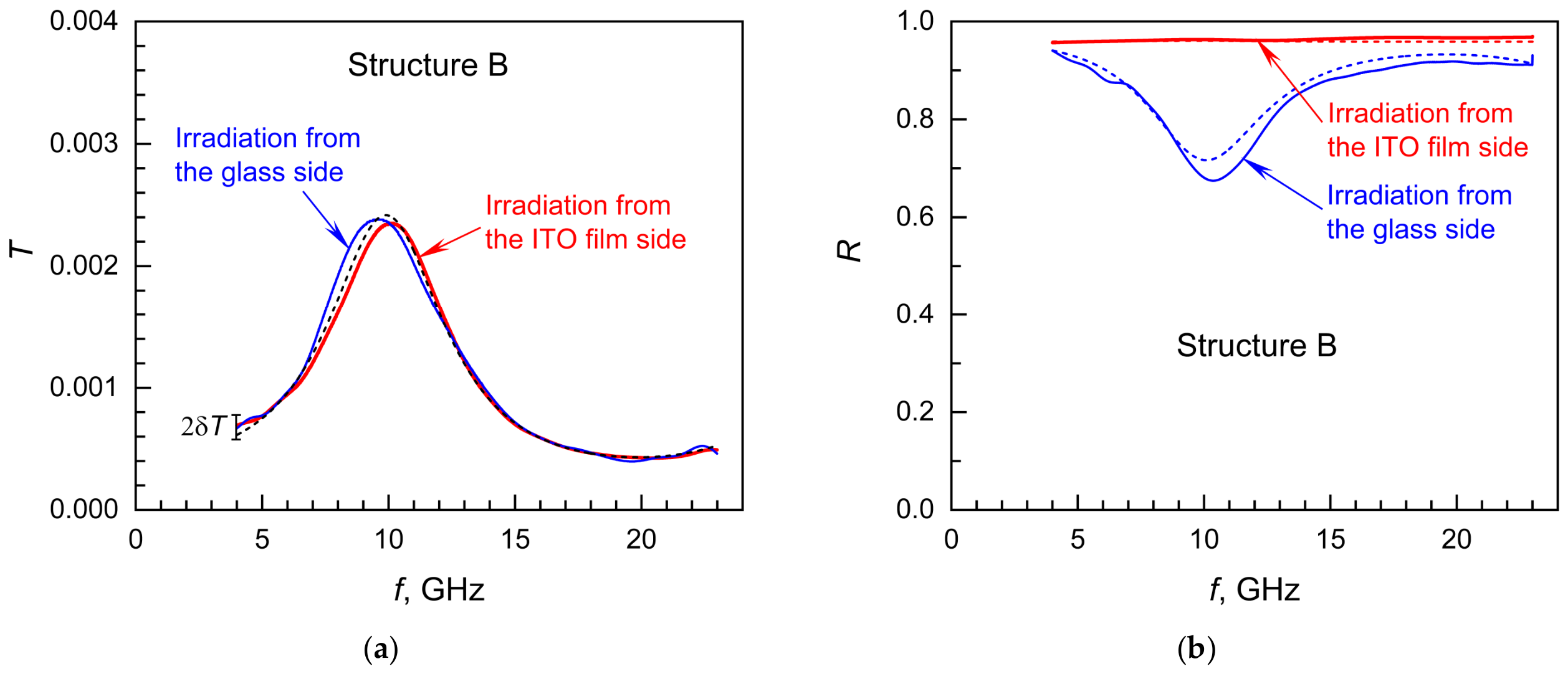
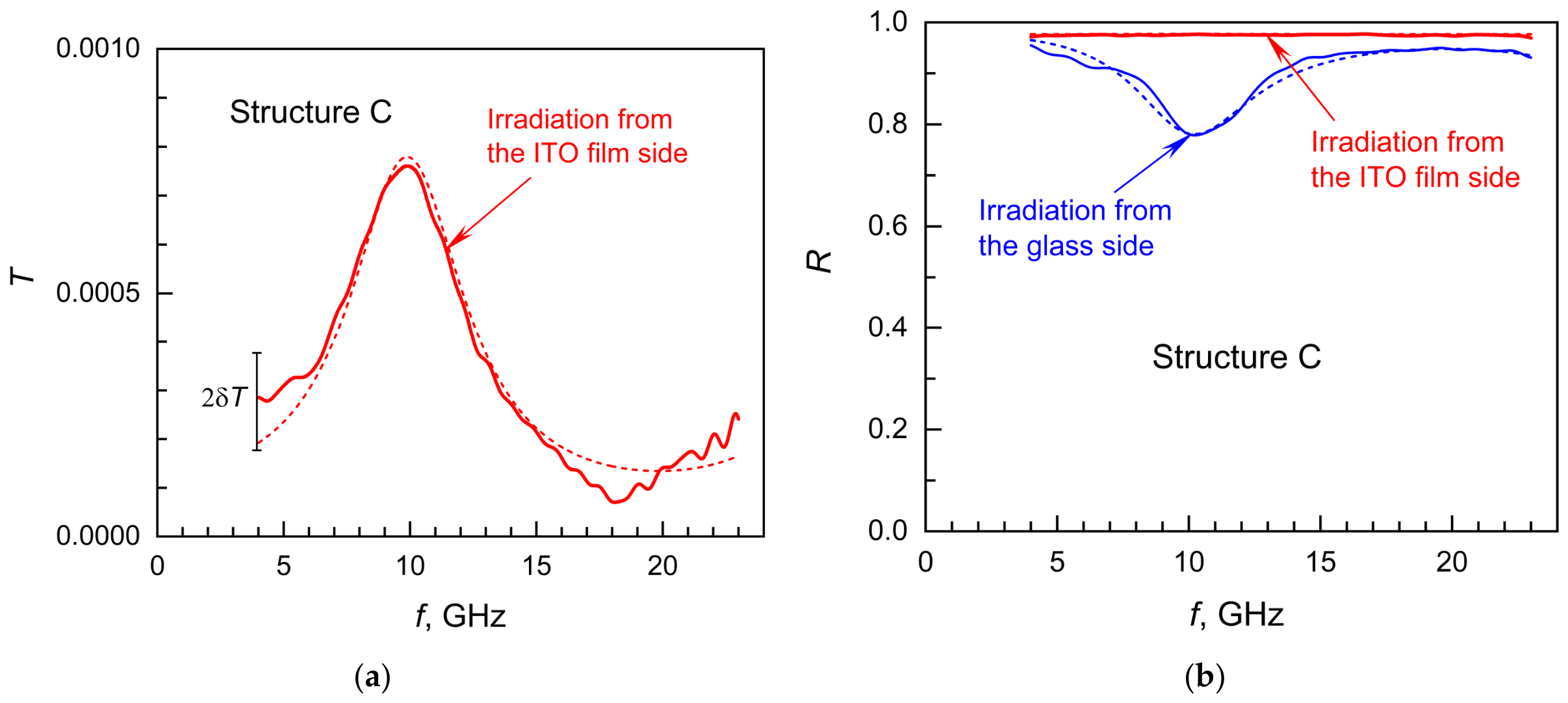
A similar analysis of the experimental microwave transmittance and reflectivity spectra was also performed for Structures B and C. The spectra for these structures (see solid lines in
Figure 8 and
Figure 9) are qualitatively similar to the spectra for Structure A. Since the thickness of the glass substrate is the same for all structures, the studied spectra preserve the spectral positions of all extremes. At the same time, the absolute values of transmittance
and reflectivity
, at any given frequency, change significantly with a decrease in the DC sheet resistivity of the ITO film.
By fitting the model microwave transmittance spectra to the experimental spectra, the value of the DC sheet resistivity
of the ITO film for Structures B and C, namely, (4.0 ± 0.4) and (2.3 ± 0.5) Ohm/sq, respectively, was determined. For each structure, the minimum value of the objective function
, which was achieved during the fitting process, turned out to be close to the absolute experimental error
(see
Table 2), which indicates the adequacy of the model used. Note that the values of
determined from the microwave transmittance spectra of structures with a diameter of 200 mm, within the margin of error, coincide with the values found from the transmittance spectrum of the witness samples (50 mm in diameter) measured using terahertz time domain spectroscopy (see
Table 2). This enables one to predict the microwave performance of the ITO film/K108 glass structures using simple THz transmittance measurements of small-diameter samples. In principle, this avoids the need for direct measurement of microwave shielding effectiveness, which requires depositing an ITO film on a large-diameter substrate (≥200 mm) and using complex equipment for measurements in the gigahertz range.
Model microwave transmittance and reflectivity spectra for Structures B and C, simulated at best-fit parameters, are shown in
Figure 8 and
Figure 9 by dashed lines. The figures illustrate that the model spectra are in satisfactory agreement with the experimental ones. Coefficients of determination for these spectra are quite close to 1. Namely, R
2 = 0.987 and 0.934 for the transmittance spectra of Structures B and C, respectively (see
Table 2). For the reflectivity spectra under structure irradiation from the glass side, R
2 = 0.924 and 0.945 for Structures B and C, respectively.
Microwave shielding effectiveness is usually determined as
. According to the simulation results (
Section 2), the transmittance
of the ITO film/K108 glass structure takes minimum values near the frequencies corresponding to the interference minima of the zero and first orders. Accordingly, in these spectral regions, the microwave shielding effectiveness will reach its maximum values.
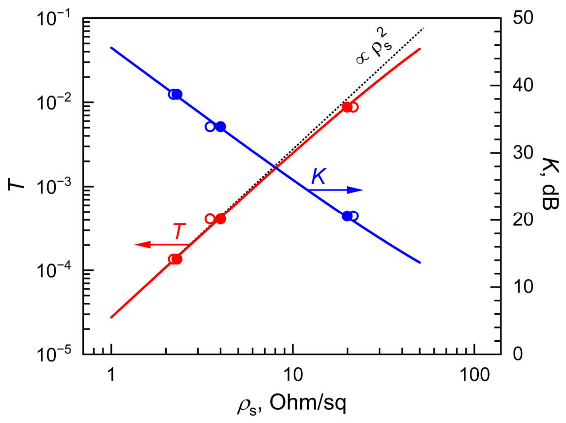
Figure 10 shows the results of calculating
T and
in these spectral regions for the shielding filters depending on the DC sheet resistivity of the ITO film at a constant glass thickness (3 mm). As noted in
Section 2, by changing the thickness of the glass substrate within the range of 1.5–4.5 mm, it is possible to move the frequency region of effective suppression of electromagnetic radiation within the frequency range from 0 to 23 GHz.
At small DC sheet resistivities ( Ohm/sq), the dependence tends asymptotically to the quadratic function (the same dependence is typical for a free-standing film). When decreases from 5 to 1 Ohm/sq, the model calculation predicts an increase in the microwave shielding effectiveness from 31.8 to 45.6 dB.
The results of the experimental determination of
and
for Structures A, B, and C are shown by circles in
Figure 10. Filled circles correspond to the values of
found from fitting transmittance spectra in the GHz range, while empty circles correspond to the values of
determined from THz TDS measurements (see
Table 2). It should be noted that the use of the latter to evaluate the microwave shielding effectiveness of the ITO film/K108 glass structures using the model discussed in
Section 2 provides accuracy of at least 0.7 dB. The maximum value of the microwave shielding effectiveness in our experiments was 38.7 dB (in Structure C).
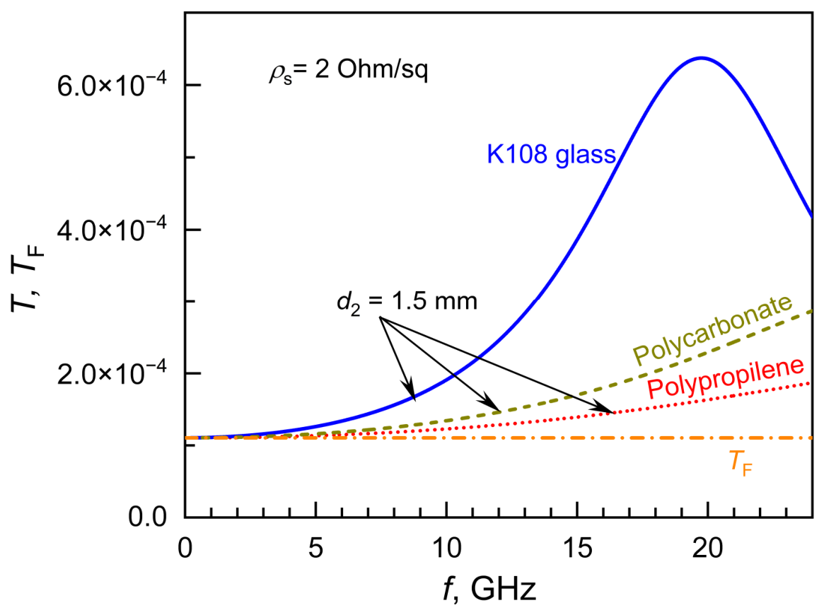
We also conducted a theoretical simulation of the ITO film-based microwave shielding filters using alternative substrates. It has been found that using transparent substrates with a lower static dielectric constant can improve the filter performance.
Figure 11 shows, for example, simulated transmittance spectra for shielding filters with identical ITO films (
= 2 Ohm/sq) deposited on 1.5 mm-thick substrates made of different materials: (i) K108 glass with a static dielectric constant of
(0) = 6.35, (ii) polycarbonate with
(0) = 3.0, and (iii) polypropylene with
(0) = 2.1.
Polypropylene provides relatively low transmission over the entire frequency range from 0 to 23 GHz, which is of interest to us: = (1.1–1.8) × 10−4; however, it does not have high enough transparency in the visible region of the spectrum, so it is impractical to use it as a substrate for ITO-based microwave shielding filters. Polycarbonate seems to be a more suitable substrate material. It has a good transparency in the visible region of the spectrum (~0.9) and, at the same time, when a conductive ITO film is applied to it, provides significantly more effective suppression of microwave radiation compared to the K108 glass filter (by 1.7–2.8 times in the frequency range from 12 to 23 GHz). Thus, using material with a lower static dielectric constant as a substrate makes it possible to expand the frequency range in which the ITO film-based shielding filter effectively suppresses microwave radiation.
4. Increasing Transparency of the Shielding Filters in the Optical Range Using Antireflective Coatings
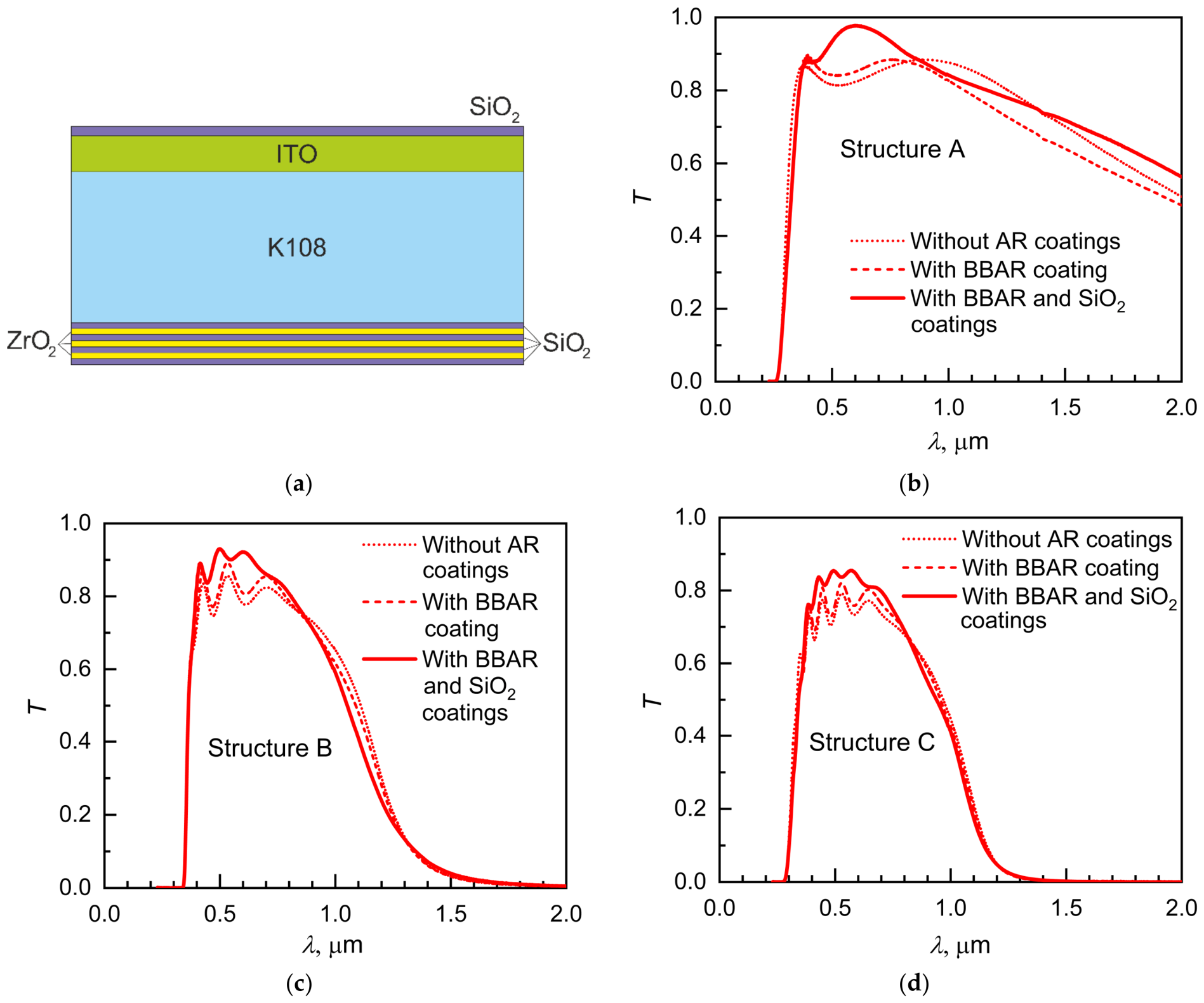
To increase the transparency of the ITO film/K108 glass microwave shielding filters in the optical range, the filters were additionally covered with antireflective (AR) coatings. Witness samples with a diameter of 50 mm were used for these studies.
First, a multilayer broadband antireflective (BBAR) coating was deposited onto the back side of the glass substrate of each shielding filter. The coating consisted of seven alternating layers of SiO2 (4 layers) and ZrO2 (3 layers). Then, a SiO2 antireflective coating was deposited onto the ITO film surface of all filters.
The optical range performance of the microwave shielding filters was examined on three types of samples: (i) ITO film/K108 glass structure without any AR coatings, (ii) the same structure after application of multilayer BBAR coating, and (iii) the structure with SiO2 coating in addition to BBAR coating. Such samples were made on the basis of each of the structures A, B, and C.
Figure 12 presents experimental transmittance spectra of the microwave shielding filters in the wavelength range from 0.25 to 2.0 microns, which completely covers the visible region of the spectrum and partially the ultraviolet and near-infrared regions. The spectra of samples with antireflective coatings are qualitatively similar to the spectra of the ITO film/K108 glass structures without AR coatings, which were previously studied in detail in [
16].
In all samples in the visible spectral range (0.4 µm <
< 0.8 µm), transmittance oscillations were observed due to the Fabry–Perot interference in the ITO film. As the DC sheet resistance of the ITO film decreased (Structure A → Structure B → Structure C), the oscillation period decreased, reflecting an increase in the thickness of the film
(see
Table 1). The bandwidth of the samples was restricted from the long-wavelength side by the free-electron absorption. As the DC sheet resistivity of the ITO film decreased, the long-wave transmission cutoff shifted towards short wavelengths, reaching
≈ 1.2 μm at
= 2.3 Ohm/sq (Structure C). A short-wave transmission cutoff, observed at
≈ 0.28–0.35 µm, is associated with interband absorption in ITO.
It is convenient to characterize the performance of the microwave shielding filters in the visible spectral region by the transmittance value averaged over the wavelength range from 0.4 to 0.8 microns. As the DC sheet resistivity of the ITO film decreases from 21.5 to 2.2 Ohm/sq, structures without AR coatings demonstrate a decrease in the average optical transmittance from 0.84 to 0.74 (see
Table 3) due to an increase in the free electron absorption.
After applying multilayer BBAR coating to the free surface of the glass substrate, the average optical transmittance of the shielding filters increases very slightly: for example, from 0.74 to 0.76 in Structure C and from 0.80 to 0.83 in Structure B. However, subsequent application of SiO2 AR coating on top of the ITO film results in a noticeable increase in the average optical transmittance: up to 0.81 in Structure C and up to 0.88 in Structure B.
On the one hand, Structure C is somewhat inferior to Structure B in terms of radiation transmission in the operating visible region of the spectrum, but on the other hand, it protects 3 times better from the unwanted effects of microwave radiation (see
Figure 10). Calculations show that a further decrease in the DC sheet resistivity of the ITO film to 1 Ohm/sq can provide a decrease in the transmittance of the shielding filter in the microwave range to 2.8 × 10
−5, which corresponds to the microwave shielding effectiveness of 45.6 dB. However, at the same time, the average transmittance in the visible spectral region drops below 0.7 (even when using BBAR and SiO
2 coatings).
5. Conclusions
The interaction of electromagnetic radiation with indium tin oxide films in the microwave spectral range has been studied experimentally. The transmittance and reflectivity spectra of the ITO films deposited on a borosilicate glass substrate have been measured in the frequency region from 3 to 23 GHz. Measurements were performed for two experimental configurations: (i) under normal incidence of microwave radiation at the ITO film surface and (ii) under incidence of the radiation at the glass surface. The transmission spectra were the same in both cases, while the reflection spectra were significantly different. The transformation of the spectra was studied when the DC sheet resistivity of the ITO film decreased from ~20 to 2.3 Ohm/sq.
Theoretical modeling of the spectra for ITO film/K108 glass structures was performed by means of the transfer matrix method using the Drude model for the dielectric permittivity of ITO and experimental data on the complex refractive index of K108 glass.
The model spectra reproduced well all the features of the experimental microwave range spectra. It was shown that for a given thickness of the glass substrate, the transmittance and reflectivity spectra of the ITO film/K108 glass structures were fully determined by only one parameter of the ITO film, namely, its DC sheet resistivity.
At a given DC sheet resistivity, the transmittance of the ITO film/K108 glass structure periodically changed with the frequency; the period of this change coincided with the period of the interference pattern in the transmittance spectrum of the glass substrate without the ITO film. However, the interference pattern in the transmittance spectrum of the ITO film/K108 glass structure is phase-shifted by with respect to the interference pattern in the glass substrate without the ITO film.
In particular, for extremely low frequency, the transmittance of the glass substrate without the ITO film reached a maximum value, while the transmittance of the ITO film/K108 glass structure reached a minimum value (zero-order interference minimum). The first-order interference minimum on the transmission curve of the ITO film/K108 glass structure with a glass thickness exceeding 2 mm had a frequency less than 23 GHz.
According to calculations, varying the thickness of the K108 glass within 1.5–4.5 mm makes it possible to achieve a transmission level close to the minimum at any point in the microwave range from 0 to 23 GHz.
A simulation of microwave shielding filters based on ITO films has been performed using alternative substrates with a static dielectric constant less than that of K108 glass. It is shown that in this case, the frequency region in which the shielding filter based on ITO film effectively suppresses microwave radiation can be significantly expanded.
According to the simulation results, the minimum microwave transmittance of an ITO film deposited on the K108 glass substrate decreased from 6.6 × 10⁻⁴ to 2.8 × 10⁻⁵ Ohm/sq, and the maximum microwave shielding effectiveness increased from 31.8 to 45.6 with a decrease in from 5 to 1 Ohm/sq. The results of the experiments confirm this conclusion. It was shown that the contactless method for determining using THz TDS measurements provided accuracy sufficient to predict microwave shielding effectiveness with an error of no more than 0.7 dB. THz TDS measurements can be carried out on ITO film/K108 glass structures of small diameter (50 mm or less), which, in principle, avoids direct measurements of microwave shielding effectiveness, which require the manufacture of test structures of large diameter (~200 mm) and the use of complex measuring equipment.
Studies have been conducted on the possibility of increasing the transparency of the ITO-based microwave shielding filters in the optical spectral range by means of antireflective coatings. A multilayer SiO2–ZrO2 BBAR coating was deposited onto the back side of the glass substrate of each shielding filter, while a SiO2 antireflective coating was deposited onto the surface of the ITO film.
It has been experimentally demonstrated that by applying such coatings to the ITO film/K108 glass structure with a sheet film resistivity of 2.3 Ohm/sq, its average transmittance in the visible spectral region increased from 0.74 to 0.81.
The results of the conducted research make it possible to find a balance between microwave shielding effectiveness and transmittance in the optical range when creating ITO-based microwave shielding filters for specific applications.



 ,
,