Article

Analysis and Design of a Transient-State Resonant Converter Used as a Frequency Multiplier

by
Josué Lara Reyes
1,
Mario Ponce-Silva
1,*,
Leobardo Hernandez-Gonzalez
2,*,
Claudia Cortés-García
1,
Jazmin Ramirez-Hernandez
2,
Susana E. DeLeon-Aldaco
1,
Oswaldo Ulises Juarez-Sandoval
2 and
Ricardo E. Lozoya-Ponce
3
1
Tecnológico Nacional de México-CENIDET, Av. Palmira s/n, Col. Palmira, Cuernavaca 62490, Mexico
2
Escuela Superior de Ingeniería Mecánica y Eléctrica, Unidad Culhuacan, Instituto Politécnico Nacional, Av. Santa Ana No. 1000, Col. San Francisco Culhuacan, Mexico City 04430, Mexico
3
Tecnológico Nacional de México-I.T. de Chihuahua, Av. Tecnológico #2909, Chihuahua 31200, Mexico
*
Authors to whom correspondence should be addressed.
Appl. Sci. 2025, 15(6), 3346; https://doi.org/10.3390/app15063346
Submission received: 3 February 2025 / Revised: 7 March 2025 / Accepted: 14 March 2025 / Published: 19 March 2025
(This article belongs to the Special Issue New Challenges in Low-Power Electronics Design)

Abstract

:

Featured Application

This work has several applications, in this case the idea is applied to an inductive wireless power transfer (IPT), in this application as larger the operation frequency more efficient the power transfer.

Abstract

The main contribution of this paper is to show the analysis and design of a resonant converter which was designed to operate in the transient stage and with underdamped response, where the resonant network stage has a frequency equal to “n” times the frequency of the switching stage (fsw) “fo = nfsw”. The main advantage of this design methodology is to be able to operate the converter with frequencies higher than 1 MHz in the resonant network stage, without obtaining high levels of losses in the inverse stage. To validate this design methodology, a full bridge resonant converter acting as a frequency multiplier was implemented for a low power wireless power transmission application. For the experimental tests, a base frequency of 300 kHz was decided in the inverting stage, with a frequency multiplication of n = 3, 5, 7 in the resonant network stage (900 kHz, 1.5 MHz, 2.1 MHz) for an output power of 12 watts. Experimental tests proved the operation of the converter acting as a multiplier, where it was possible to reduce losses in the inverter stage, achieving efficiencies of up to 93% in the switching stage with frequencies higher than 1 MHz.

1. Introduction

In recent years, the development of electronic systems has been improving greatly, bringing improvements in different areas, but mainly in switched mode power converters used for renewable energy applications, medical equipment devices, electric cars, and smart devices. Currently, the trend in electronic circuit design is focused on reducing cost, size, and increasing power density and efficiency of electronic systems [1,2,3]. Operating at high frequencies is an excellent way to achieve these objectives since it minimizes the size of the components that store energy, which reduces the cost of the overall converter and enhances the power density. Resonant converters are commonly employed in these applications because they allow for high frequency operation and soft switching, which significantly reduces switching losses [4].
The issue with these types of converters is that operating at frequencies above 1 MHz typically necessitates the use of expensive electronic cards in the control stage, special semiconductors, and control methods applied to the inverter/rectifier stage, increasing the circuit’s total cost and complexity [5].
Typically, resonant converters are designed in a steady state and analyzed using the first harmonic approximation method, which is a modeling methodology that assumes only the first harmonic signal contributes to power transfer [6,7]. The performance of resonant circuits operating in the transient state has not received much attention, and it is quite interesting to see what applications the analysis of resonant circuits operating in the transient state can be utilized for [8].
This paper presents the analysis and design in the transient state of a resonant converter acting as a frequency multiplier, where the oscillation frequency of the current in the resonant tank is equal to “n” times the switching frequency at the inverter stage (fo = nfsw), allowing it to operate at high resonant frequencies in the resonant network without needing a high switching frequency in the inverter. The concept of frequency multipliers is not new; numerous publications have already been published.
A frequency multiplier is a DC circuit in which the frequency of the output signal is a harmonic component of the frequency of the supply signal. If the frequency of the input signal is “fsw”, a resonant tank can be used to filter out the unwanted frequency components and leave only the signal component whose frequency is “nfsw” at the output [9,10,11,12]. These circuits are commonly utilized in high-frequency RF applications where parasitic semiconductor components limit the maximum working switching frequency, such as switched mode inverters and power amplifiers.
Unlike conventional frequency multipliers, which require decomposing a signal with harmonic content and then filtering out unwanted harmonics using bandpass circuits, the methodology presented in this work achieves frequency multiplication naturally through the underdamped transient response of a series RLC circuit. This approach eliminates the need for additional filtering and simplifies circuit design, allowing for higher power levels and reducing losses compared to conventional harmonic filtering-based frequency multipliers.
These frequency multiplication approaches have been presented in the design of DC-DC converters, but they are not widely used since the output power of a frequency multiplying inverter is intrinsically low when compared to the ratings of the needed devices. The low power levels at which frequency multipliers usually work limit the applications in which they can be used, being used only in radio frequency applications, which is where power levels in the order of milliwatts are usually handled [13,14,15,16].
The transient design methodology presented in this work allows a resonant converter to act as a frequency multiplier, where the operating power is not limited only to low levels and brings advantages in the operation of the converter as well as in the reduction of losses in the switching stage. This design methodology is different from the harmonic selection technique for frequency multiplication, which has already been studied and applied to wireless power transmission [17,18,19]. It is important to clarify that this methodology is not aimed at communication applications, where frequencies in the GHz range are common. Excessively multiplying frequency would require extremely large inductors and very high-quality factors, impacting efficiency. This proposal mainly targets practical applications requiring relatively high frequencies (MHz) while using lower frequencies at the switching stage, ideal for wireless power transfer, induction heating, and wireless charging of electric vehicles.
The theoretical analysis of the multiplier circuit designed in transient and with underdamped response was presented in [20], where the operation of a series RLC circuit acting as a frequency multiplier was verified by simulation in SPICE, which reached the established operating parameters. This prior work provided the fundamental understanding of how the transient response of an underdamped RLC circuit could be leveraged to achieve frequency multiplication, without requiring harmonic filtering or direct high-frequency switching. The insights gained from this analysis were instrumental in developing the transient design methodology for the resonant converter presented in this work, extending the theoretical findings into a practical implementation.
In this work, the analysis presented was used for the development of the transient design methodology of the resonant converter acting as a multiplier, since, as shown in Figure 1, it is only necessary to replace the bipolar DC voltage source by a full-bridge inverter in order to apply the transient analysis in a resonant inverter and then in a resonant converter. A detailed literature review revealed that no previous studies have reported resonant converters explicitly designed to operate in transient conditions. Existing works primarily focus on steady-state analysis using methods such as the First Harmonic Approximation (FHA) or other conventional modeling techniques. Therefore, this work represents the first experimental validation of a resonant converter designed specifically for transient operation, marking a novel contribution in the field of high-frequency power electronics.
The resonant converter designed to operate in the transient state presented in this work was used in a wireless power transmission application, which is a currently relevant application and where the performance of the converter could be verified, since usually in this type of applications very high operating frequencies are required, with low levels of losses mainly in the switching stage.
The converter complied with the established operating parameters, which were verified first by simulation in SPICE, and then during the experimental tests. The transient operation allowed to greatly reduce the losses in the switching stage, because it was possible to operate with a frequency much lower than the one present in the resonant tank. Regarding the losses in the inductive coupling between the transmitter-receiver inductor pair, these are not affected to a great extent by the transient operation, as well as the losses in the rectification stage, which was the one with the highest losses due to the high operating frequencies at which the rectifier was exposed.
The transient operation to operate the resonant converter as a frequency multiplier only brought benefits to the inverter stage, which is in charge of providing the base switching frequency fsw. The analysis and design methodology used in this work, as well as the results obtained after the experimental tests, are presented below.

2. Resonant Converter Transient

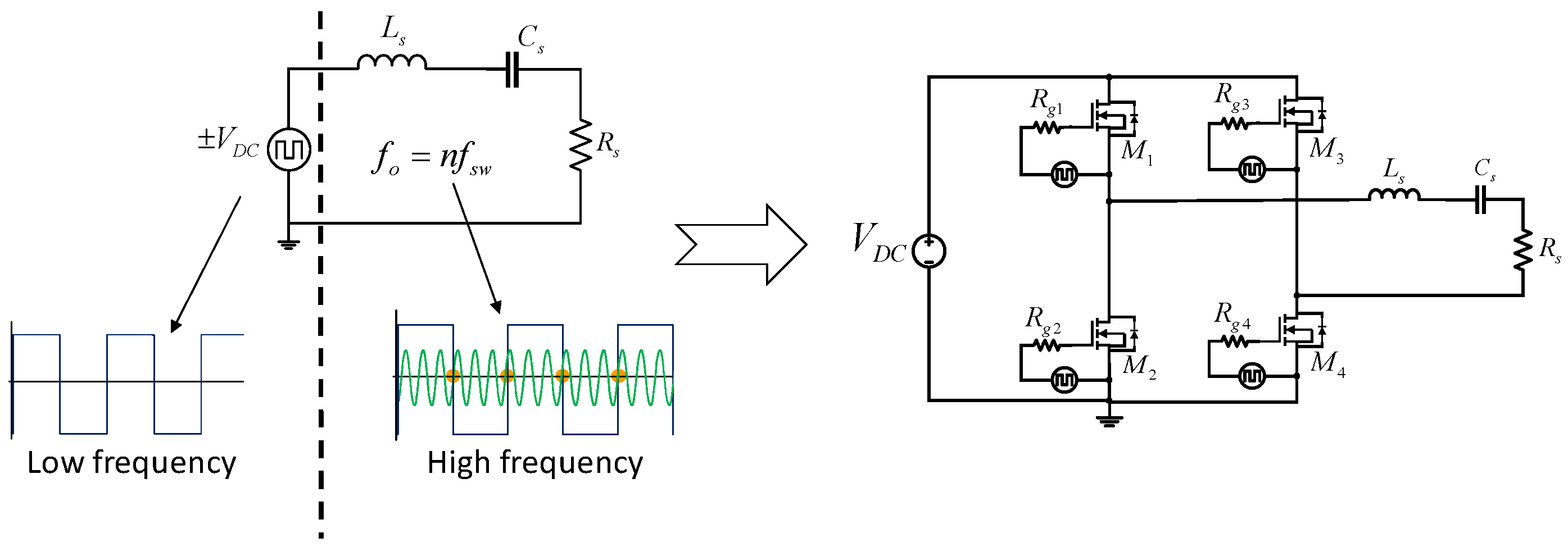
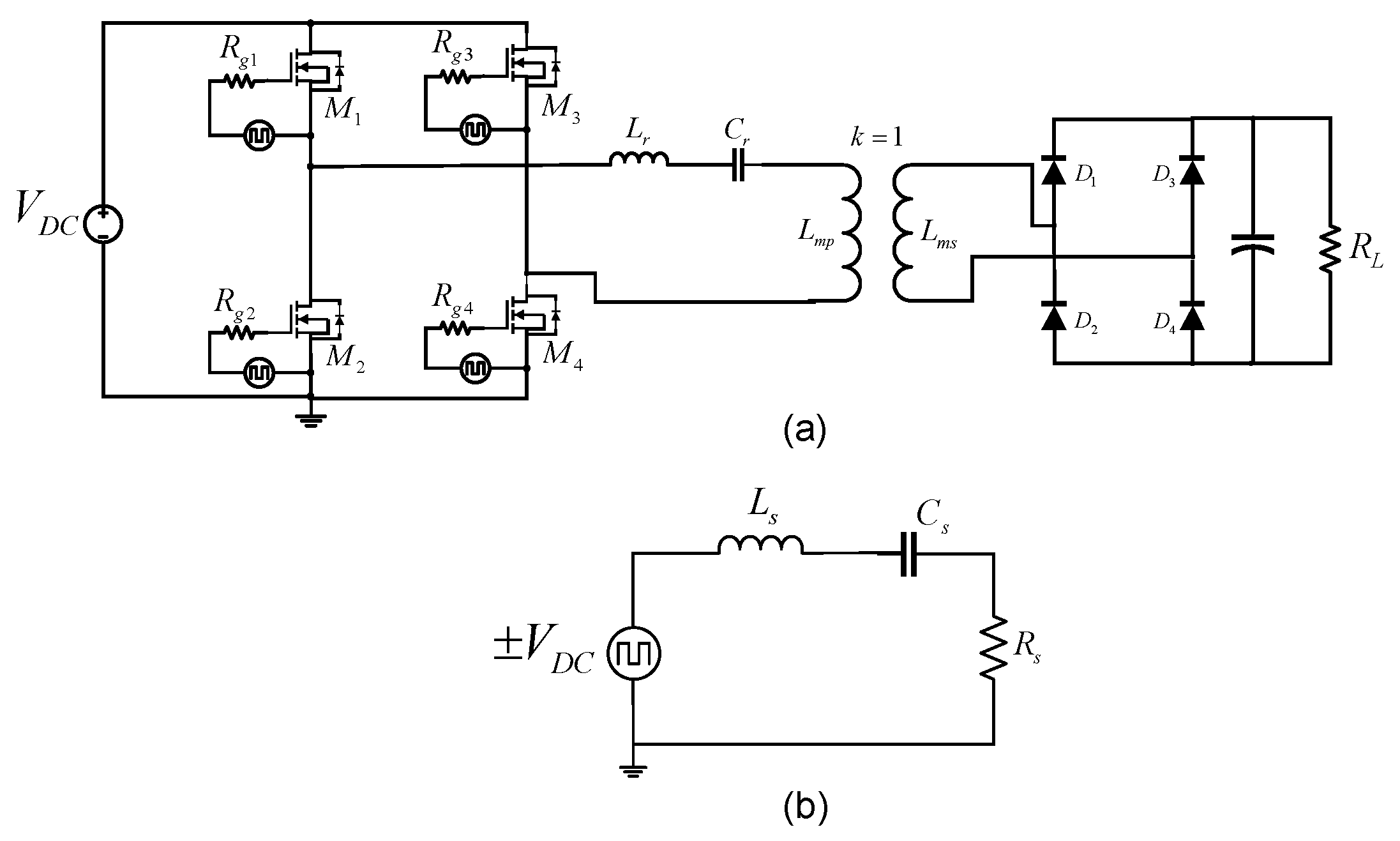
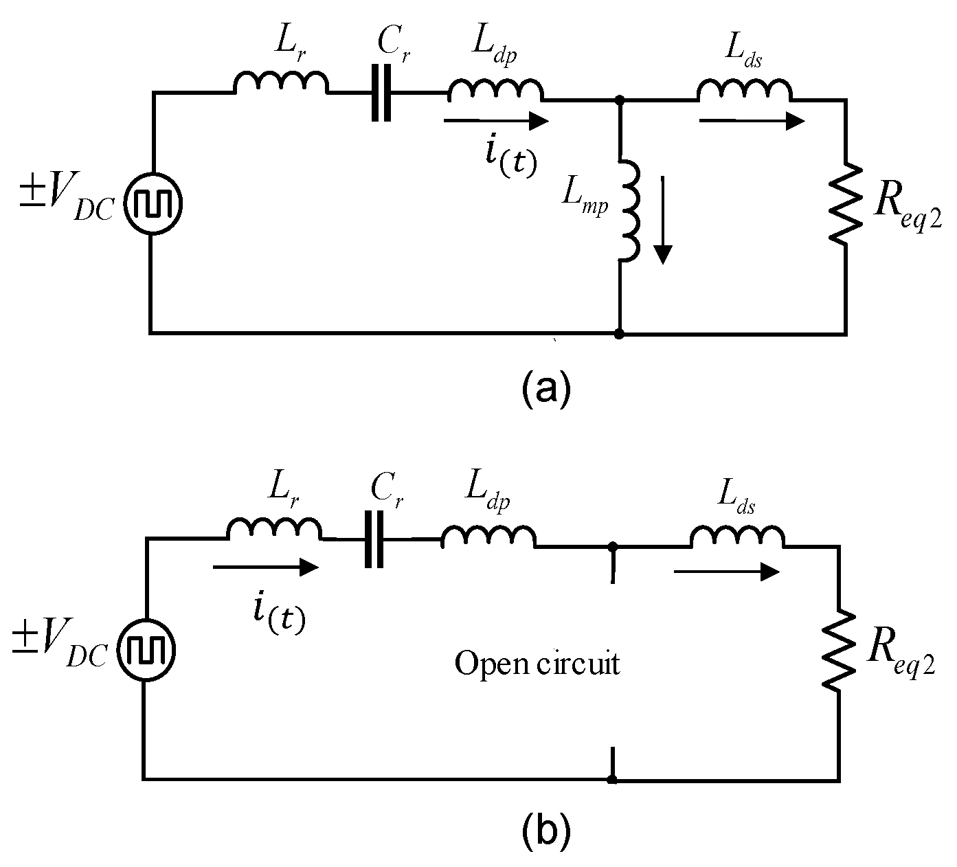
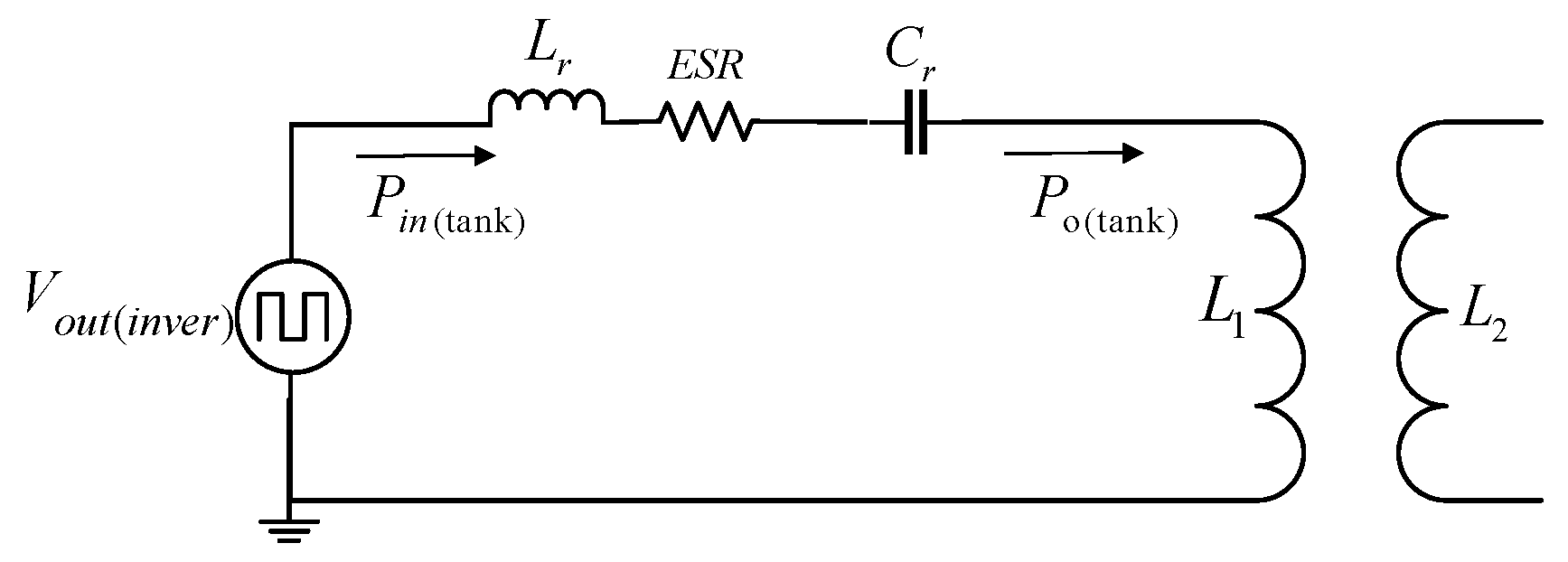
2.1. Determination of Equivalent Circuits for Transient Design of the Resonant Converter

The design methodology of the transient resonant converter in Figure 2a consisted of determining the equivalent circuits of each stage of the converter until reaching the equivalent RLC circuit in series, as shown in Figure 2b, where the transient analysis shown in [17] is applied.
The analysis begins by replacing the output voltage of the full bridge inverter with a bipolar square voltage source. The rectifier stage and the load at the output are replaced by its equivalent resistive value “Req1” which is defined by (1). The procedure to determine Req1 is shown in detail in [2].
The equivalent circuit replacing the rectifier by its resistive value is shown in Figure 3, where the primary stray inductance Ldp and secondary stray inductance Lds are also considered to determine the following equivalent circuits. These parasitic inductances must be measured in the circuit, considering the operating frequency and the power transmission distance [18].
R e q 1 = 8 R L η r e c π 2
where RL is the load resistance at the converter output, ɳrec is the efficiency of the full bridge rectifier.
The following equivalent circuit is determined considering the magnetizing inductance Lmp and the secondary distortion inductance, as shown in Figure 4a. Performing the reactance analysis between the components Lmp, Lds, and Req2, two new equivalent components Leq1 and Rs are obtained, resulting in a series circuit as shown in Figure 4b. Equations (4) and (5) determine the reactances of the equivalent components Xleq and Rs, where in each equation the operating frequency fo is considered to be the switching frequency fsw multiplied by the multiplier “n”, as shown in (2) and (3).
f o = n f s w
ω o = 2 π f o
X L e q = X L m p X L d s X L m p + X L d s + R e q 2 2 R e q 2 2 + X L m p + X L d s 2
R s = j X L m p 2 R e q 2 R e q 2 2 + X L m p + X L d s 2
where Xlmp is the reactance of the magnetizing inductance, Xlds is the reactance of the secondary stray inductance, and Req2 is the equivalent resistance of the rectifier reflexed to the primary side, which is of the same value as Req1 ≈ Req2.
Considering the operating frequency fo in the resonant tank of the converter, the value in henries of the equivalent inductor Leq1 is determined by (6).
L e q 1 = X L e q 2 π f 0

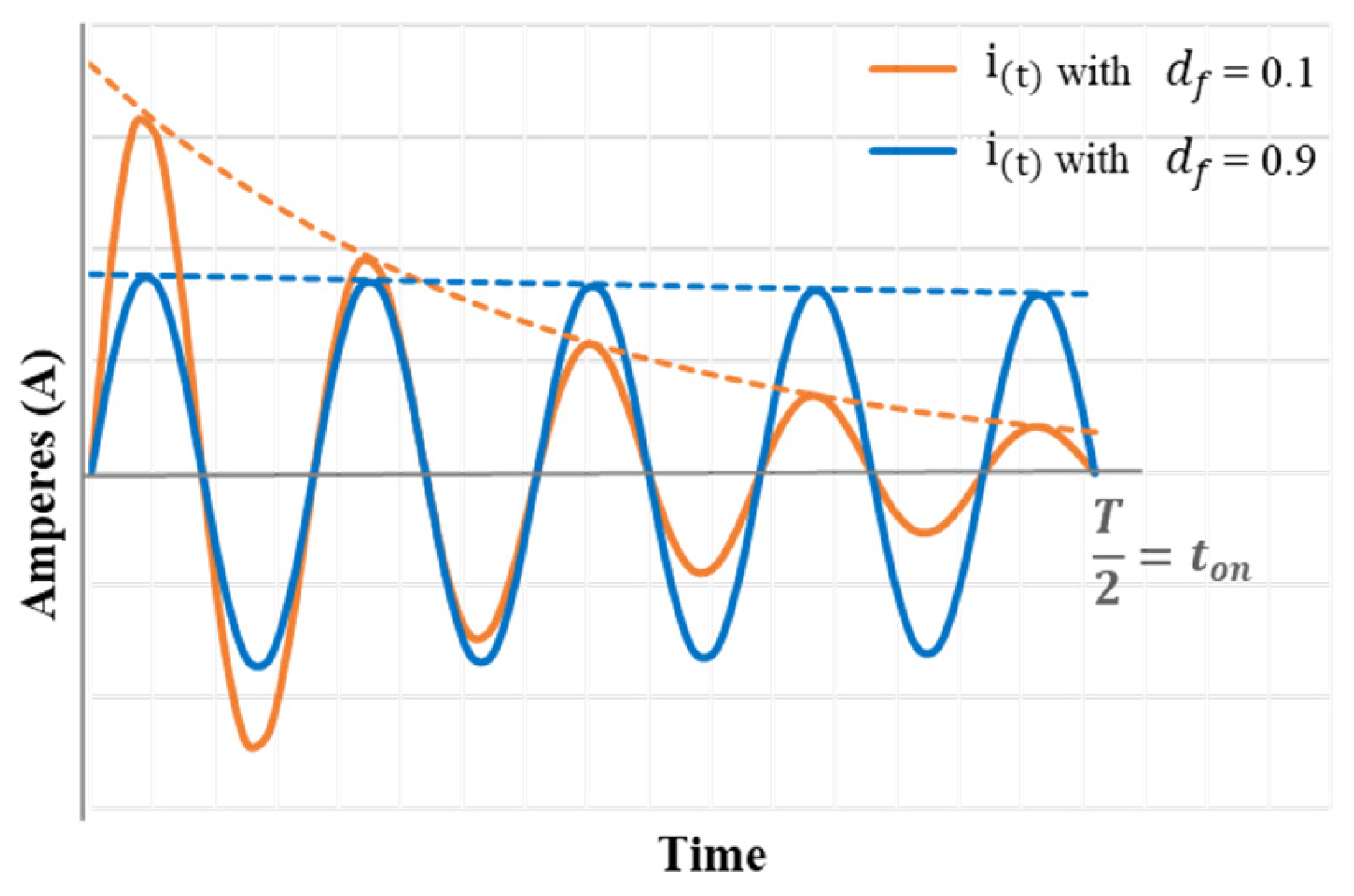
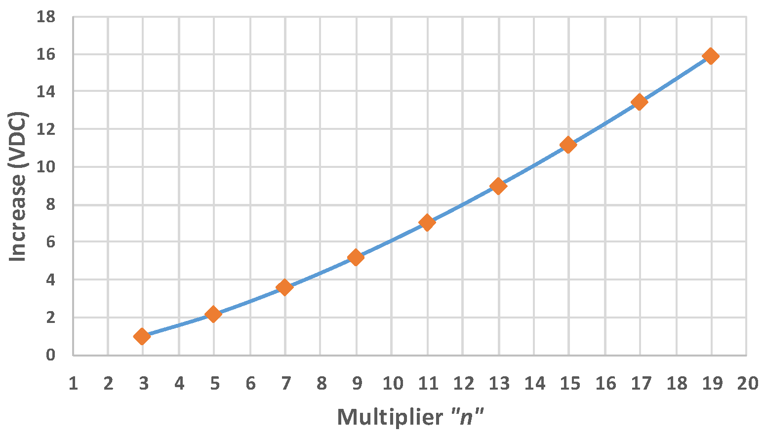
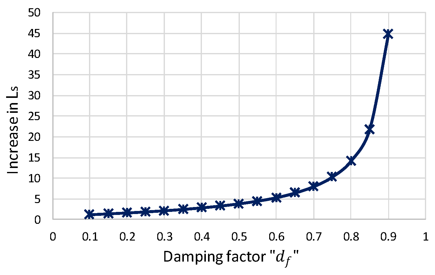
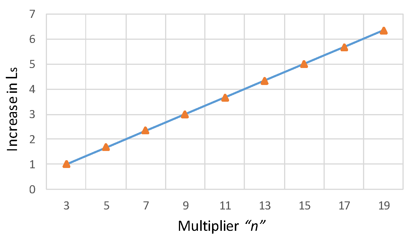
2.2. Optimization Constant “g” for Satisfying the Series Condition of the RLC Equivalent Circuit

As shown in Figure 1, the transient analysis shown in [20] is applied to a series RLC circuit, as shown in Figure 4b, so the equivalent circuit of the resonant converter in Figure 4a must act as a series circuit. Figure 5a shows the equivalent circuit where the magnetizing inductance is being considered, which affects the transient behavior and underdamped response, since, depending on the value of the resistance Req2, the current can be diverted to the magnetizing inductance, affecting the desired operation of the circuit and no longer behave as a series circuit.
To solve the drawback presented by the magnetizing inductance Lmp in the circuit, it is necessary to propose operating conditions for the current to flow only to the equivalent resistance Req2, as shown in Figure 5b.
In the circuit of Figure 5a, if the inductive reactance of Lmp is much larger than the equivalent resistance Req2, the current will flow only to Req2. Equation (7) introduces the optimization constant “g”, which proposes the necessary operating condition for the current to flow only to Req2, indicating that the value of the magnetizing reactance Xlmp is at least 10 times greater than Req2.
X L m p = ω o L m p = g R e q 2
where g is the optimization constant and its value is g ≥ 10. Considering the constant “g” in the equivalent circuit of the resonant converter, it is necessary to determine the value of the load RL necessary to satisfy the operating condition proposed by (7). Considering (7) and solving for RL:
R L = 2 π 3 f o L m p 8 g η r e c .
Equation (8) defines the value required in the RL load at the output of the resonant converter for the equivalent circuit to behave as a series RLC circuit as shown in Figure 5b.

2.3. Transient Operation of the RLC Equivalent Circuit in Series of the Resonant Converter

Considering the operating condition of (7) and the value of RL given by (8), the equivalent circuit of the resonant converter is behaving as a series RLC circuit as shown in Figure 5b.
In the circuit of Figure 5b, the total series inductance value is the sum of the inductances Lr, Ldp, and Leq1. This total series inductance value Ls in the series equivalent circuit must maintain the current oscillations in the resonant tank at the operating frequency determined by the multiplication between the inverter frequency and the multiplier fo = nfsw, where the switching frequency fsw and the multiplier “n” are values set in the operating parameters of the inverter. Equation (9) determines the value of Ls.
L s = L r + L d p + L e q 1 = D R s a 2 n f s w π
where D is the inverter duty cycle, Rs is the total series resistance in the equivalent circuit, n is the frequency multiplier, “a” is the underdamping constant determined.
a = π n ln d f
where df is the decay factor and defines the decay in the amplitude of the current up to the half-period of the inverter switching signal. The decay factor df is a parameter that is set in the operating specifications of the inverter and can have values from df = 0.1 − 0.9. Figure 6 shows the effect of the decay factor on the current waveform, where the higher the value, the more sinusoidal waveforms can be obtained, as shown in the blue graph in Figure 6. The decay factor is an important parameter in the transient operation of the circuit; [20] explains in detail the most important characteristics and implications.
Considering (9), it is possible to determine the value of the inductance Lr by means of (11), where Lr is the inductance in the resonant tank of the underdamped converter. The value of the capacitor that is in the resonant tank is determined by (12), where the total series inductance Ls of the equivalent RLC circuit is considered. The capacitor Cr that is in the converter tank is the same series capacitor Cs = Cr shown in the equivalent RLC circuit in Figure 2.
L r = L s L d p L e q 1
C r = 1 ω o L s

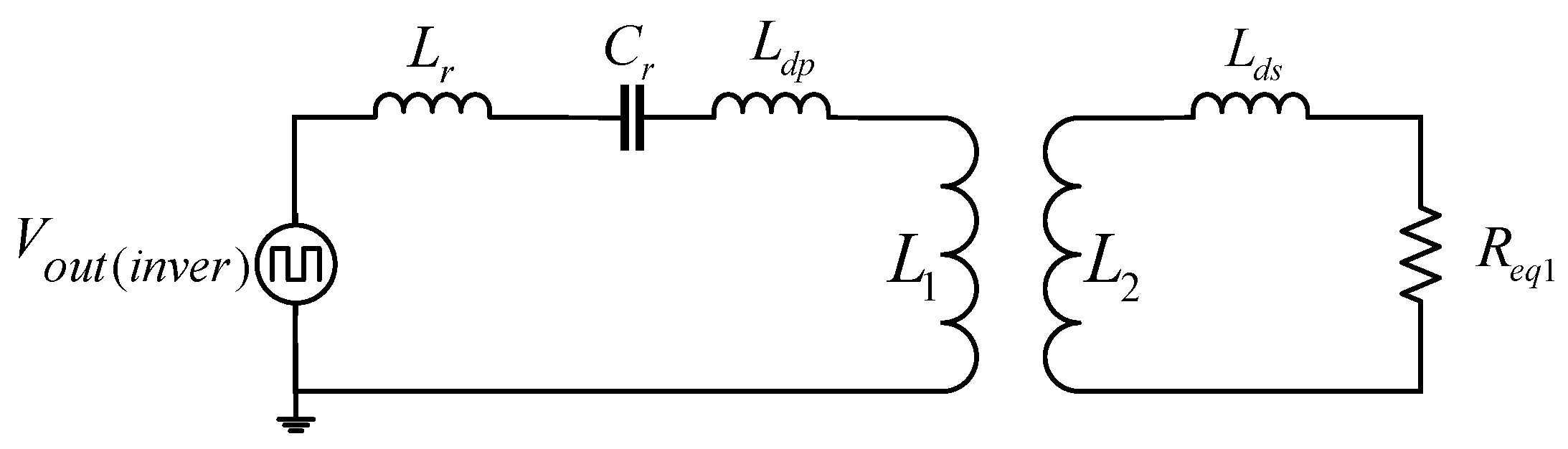
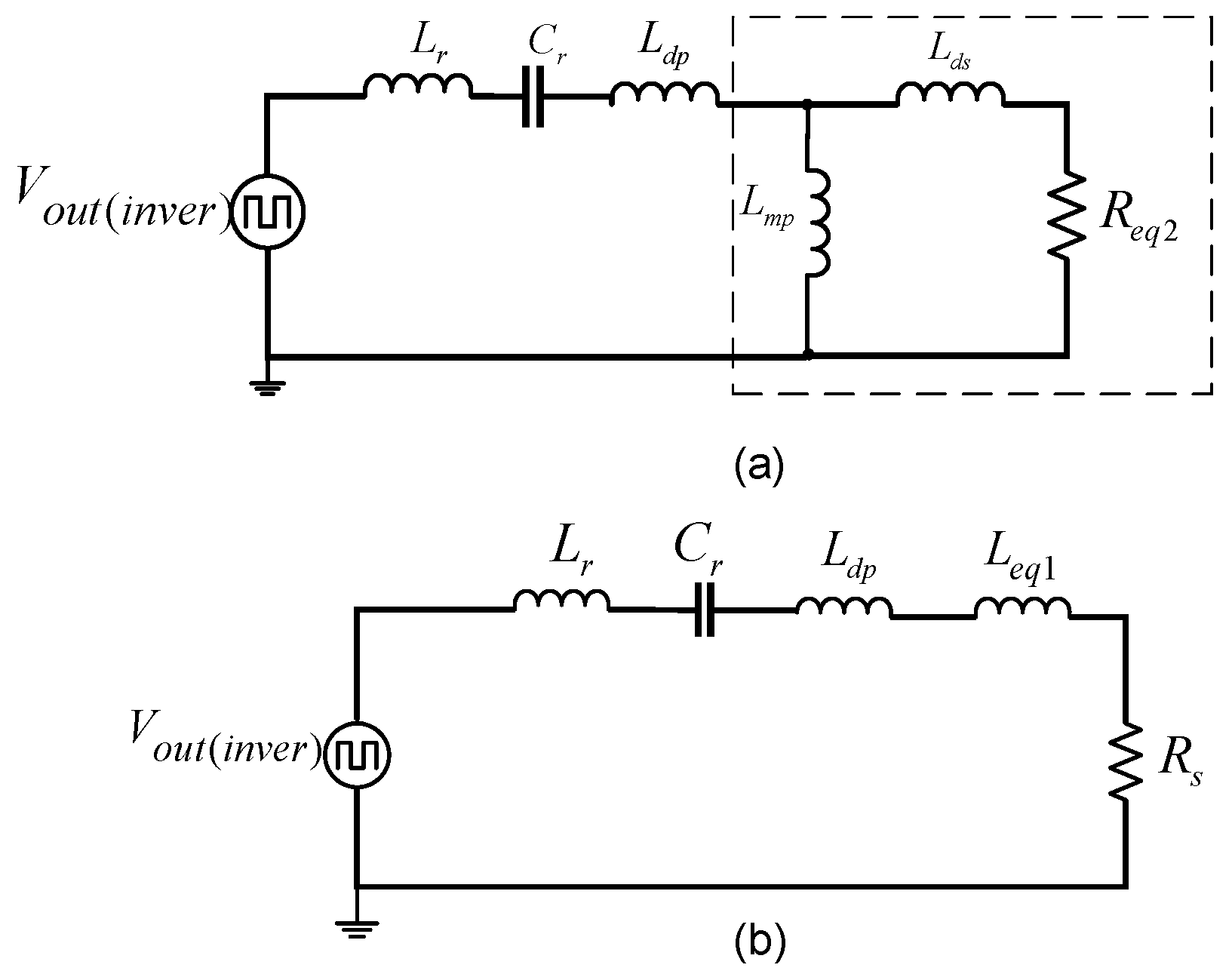
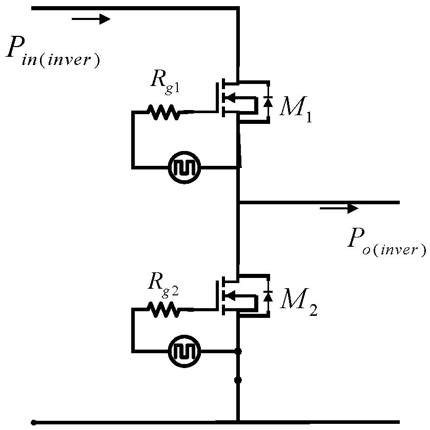
2.4. Reduction of Components in the Switching Stage

As shown in Figure 1, the equivalent series RLC circuit requires a bipolar voltage source at the input, which leads to the use of a full bridge inverter with four switches in the transient resonant converter. But, due to the series capacitor of the RLC circuit and taking into account the Fourier series decomposition of the signal, it is possible to filter the dc component of a unipolar voltage signal at the input of the circuit, allowing the use of a class D topology inverter to reduce the circuit components.
The output voltage of a Class D inverter is a unipolar voltage signal, where after removing the DC component, it behaves as a bipolar voltage signal in the series RLC circuit, with the characteristic that now the maximum voltage is divided by two. To use an inverter with unipolar output voltage like that of the Class D inverter, the same design methodology must be followed as with a bipolar source at the input of the circuit, but the DC voltage must be multiplied by two to achieve the output power set, as shown in Figure 7b. The DC voltage required for a given power output is calculated by (13).
V D C = P o R s D 2 a 2 ( 1 + c o d d ) 2 b
where Po is the output power at the load, “b” is the constant that determines the RMS current flowing in the equivalent circuit defined by (14), “c” is the constant that determines the voltage level stored by the capacitor Cr defined by (15).
b = a 1 e 2 n π a 4 n π
X C 1 + e n π a 2 D R s a X C 1 + e n π a
The topology of the resonant converter that was implemented in this work used class D inverter, which allowed reducing the conduction losses and also the total cost of the circuit. Figure 8 shows the topology of the resonant converter that was implemented and subjected to the experimental tests.

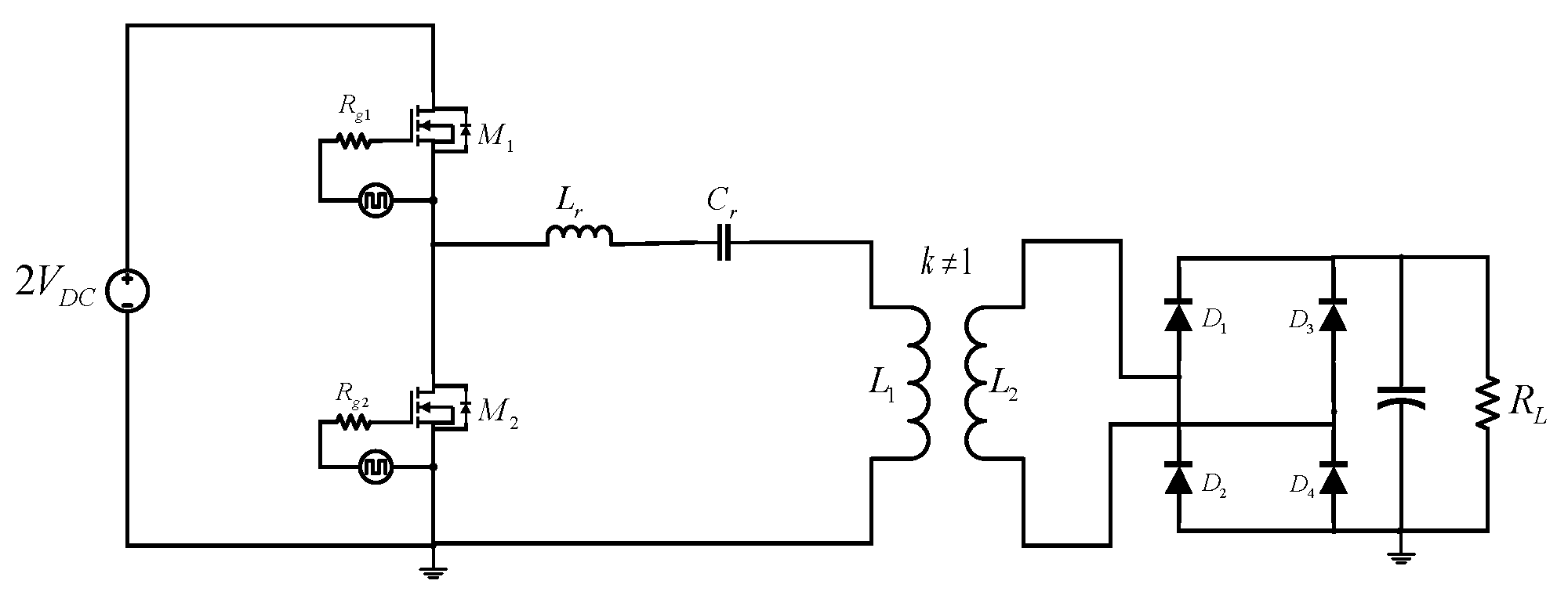
3. Design Methodology and Experimental Testing

3.1. Design Methodology and Establishment of Operating Parameters

The design methodology of the resonant converter of Figure 8 to operate in the transient state, with underdamped response and acting as a frequency multiplier, is presented below. Table 1 shows the operating specifications of the converter for experimental testing. Table 2 shows the complete transient design methodology of the converter. It is recommended to consult the work reported in [20], which explains in detail how each transient operation parameter was determined.

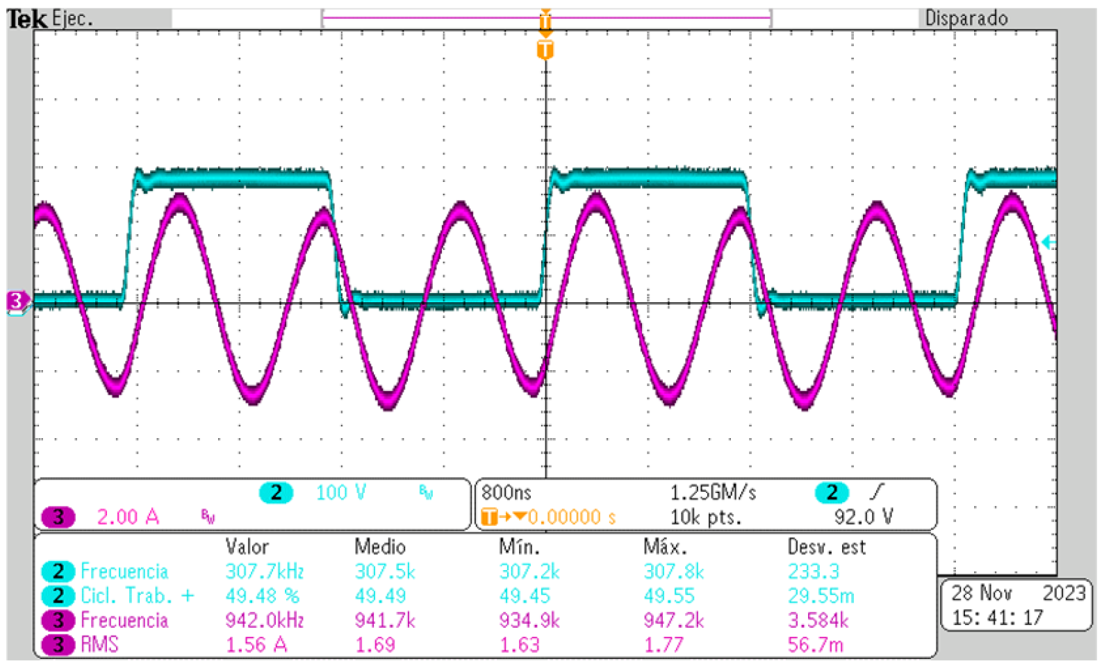
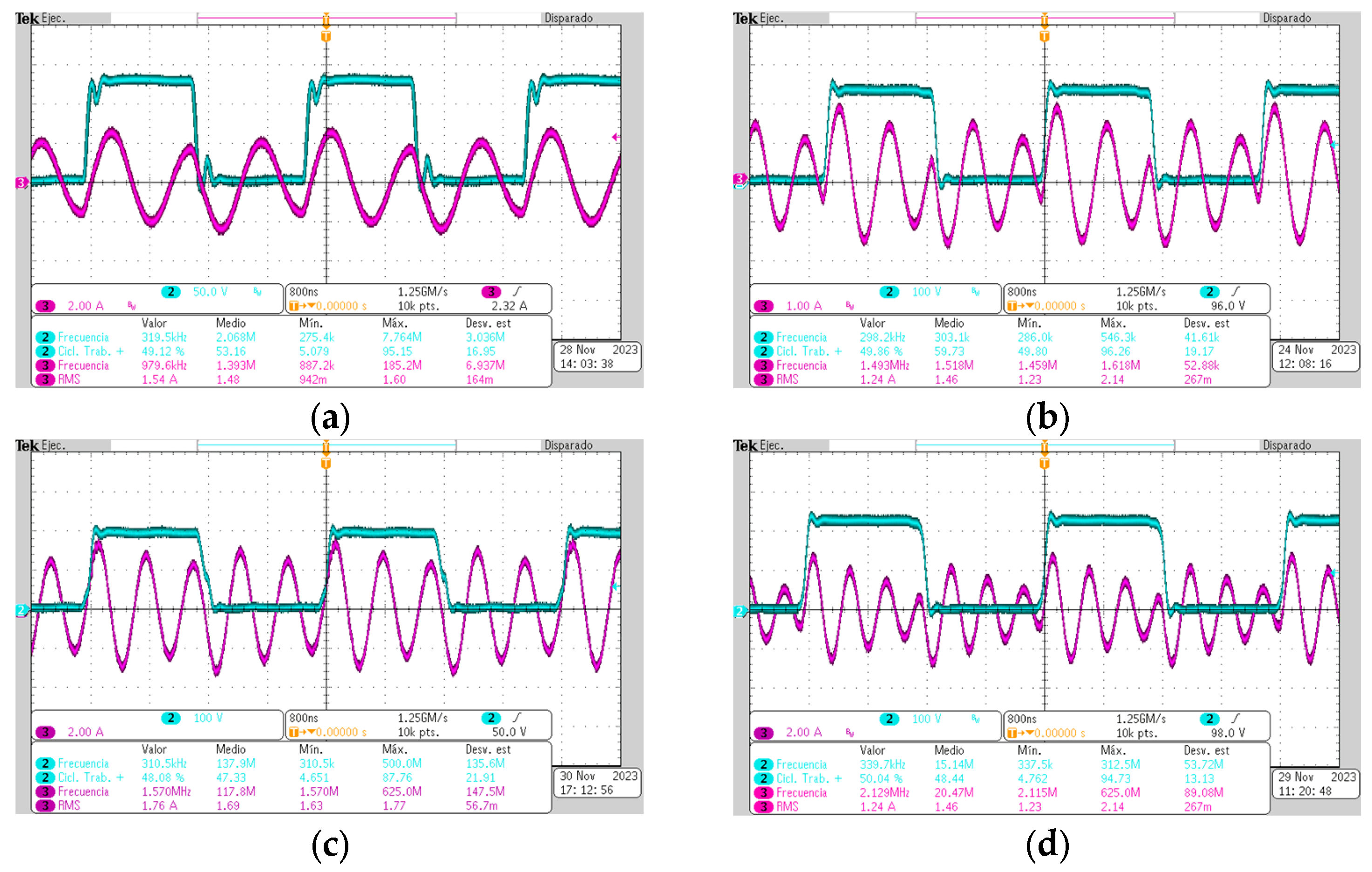
3.2. Development of Experimental Tests

To verify the operation and performance of the transient resonant converter, experimental tests of the circuit were performed. Figure 9 shows the resonant converter subjected to the experimental tests. A variable resistor was used as load on the “RL” output, and for the wireless power transfer, the pair of coupled inductors WE760308111 from Wurth Elektronik (Waldenburg, Germany) was used.
The experimental tests consisted of checking that the converter complied with the operating specifications in Table 1, in addition to checking that it was operating in the transient state and acting as a frequency multiplier in the resonant tank.
Figure 10 and Figure 11 show the oscilloscope screen captures, where it is verified that the resonant converter is operating correctly, since, as seen in Figure 10, the inverter switching frequency is fsw ≈ 300 kHz, while the frequency of the current in the resonant tank is oscillating at a frequency of fo ≈ 900 kHz, which verifies the frequency multiplication according to the value of the multiplier “n = 3”. Furthermore, the plot of the resonant tank current (purple) satisfies the value proposed by the decay factor df = 0.90, since, as can be observed, the current amplitude does not decay to a large extent until the middle of the switching signal period, preserving a completely sinusoidal waveform. Figure 11 shows the output current, power, and voltage levels, which satisfy the operating parameters.
To check the feasibility in the implementation and the performance of the transient operation, further tests were performed using values in the multiplier with n = 3, 5 ,7 and for different values in the decay factor. These tests prove that the resonant converter can act as a high frequency multiplier without limitations in the operating power level, which is one of the drawbacks of frequency multipliers where only low power values are handled.
As shown in Figure 12a–d, the current amplitude showed a slight decay up to the middle of the switching period. This was because the value in the decay factor used during the experimental tests was lower than df = 0.9 (current waveform without decay). Using low values in the decay factor such as df > 0.9, and with values in the frequency multiplier up to n = 7, allowed satisfying the established operating parameters and reaching the desired output power.
In the experimental tests, the use of air core inductors was chosen to reduce losses in the resonant tank due to magnetic hysteresis, the efficiency of the tank being only affected by the value of the parasitic series resistance ESRL of the inductor Ls.

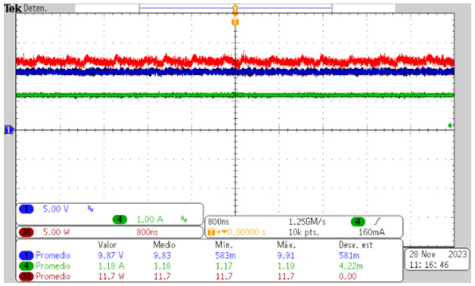
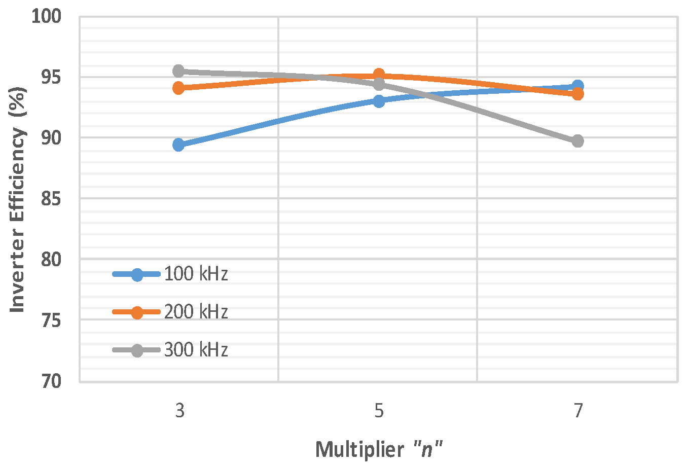
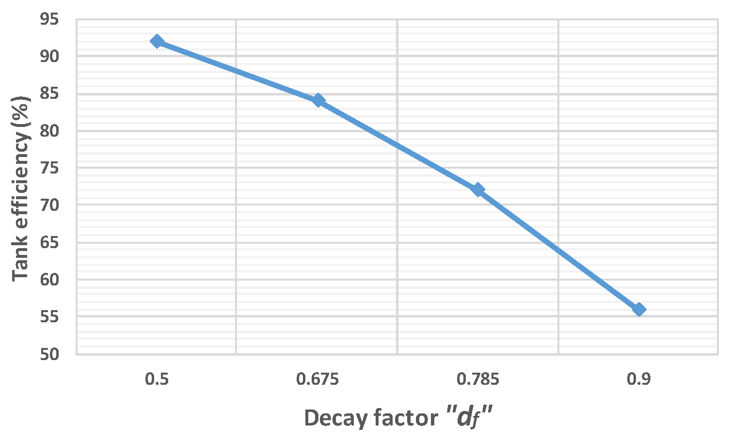
3.3. Implications on the Efficiency of the Resonant Converter Acting as a Frequency Multiplier

The resonant converter met the performance specifications and succeeded in acting as a high frequency multiplier. As shown in Figure 12a–d, tests were performed with different odd values in the multiplier and for different decay factors “df”. Using high values in the multiplier, or in the decay factor brings some implications in the circuit performance. As shown in Figure 13, increasing the value in the multiplier “n” leads to an increase in the supply voltage VDC. This is because the higher the value in the multiplier “n”, the higher the operating frequency “fo” and the higher the RL load value as indicated in (8).
The increase in the supply voltage brings with it an increase in the losses in the inverter, because the parasitic capacitances of the Mosfet are charged to the supply voltage VDC, especially the output capacitance Coss which is normally the highest capacitance. Equation (16) defines the energy in joules at which the Coss capacitance is loaded, and (17) defines the power losses in watts.
P M = 1 2 C o s s 2 V D C 2 f s w
E c o s s = 1 2 C o s s 2 V D C 2
Considering that in a class D inverter only two Mosfet switches switch in one cycle of the switching signal, the total losses of the switching stage are defined by (18).
P i n v e r = C o s s 2 V D C 2 f s w
As shown in (17), the losses increase due to the increase in the supply voltage VDC as the multiplier “n” increases, where the inverter switching frequency fsw is a fixed value and does not increase the losses in the inverter as the operating frequency fo in the resonant tank increases.
In order to check the effect on the efficiency of the converter when operating as a frequency multiplier, power measurements were made in the circuit using the digital oscilloscope, more precisely in the inverter stage and in the resonant tank, which is where the efficiency of these stages is affected due to the transient operation. The measurements in the inverter stage were performed with the switching frequencies of 100 kHz, 300 kHz, and 500 kHz. Measurements were made of the power entering Pin(inver) and the power leaving the inverter Po(inver), where the difference in power would be the losses, determined by (19).
P l o s s ( i n v e r ) = P i n ( i n v e r ) P o ( i n v e r )
Figure 14 shows the measurements made in the circuit to determine the losses in the inverter. Figure 15 shows the inverter efficiency percentages when using multiplier values with n = 3, 5 ,7. As shown in Figure 15, the lowest efficiency was obtained using the switching frequency fsw = 100 kHz, because at this frequency, the predominant losses were conduction losses due to the RMS current flowing through the resonant tank and the Rdson resistance of the Mosfet. With the switching frequencies of 200 kHz and 300 kHz, efficiencies were very close with the multiplier n = 3, and were moving away from the multiplier n = 5, where it is observed that the higher the frequency multiplication, the lower the efficiency, since the required VDC supply voltage is higher.
Regarding the efficiency of the resonant tank, it is mostly affected by the series inductance Ls, which depends on the decay factor df and the multiplier “n”. Figure 16 shows how the decay factor increases the value of the series inductance Ls needed in the circuit to operate underdamped, where using a decay factor of df = 0.9 (sinusoidal waveform) would increase almost forty-five times the value of its inductance. Figure 17 shows the increase in inductance Ls as the value of the multiplier increases, where this occurs due to the increase in the load resistance at the output RL and the increase in the equivalent series resistance Rs as the operating frequency fo in the resonant tank increases.
Figure 18 shows the measurements performed to determine the efficiency of the resonant tank, where it was necessary to measure the input power Pin(tank) and output power Po(tank). The measurements were performed with the switching frequency fsw = 300 kHz and with the multiplier n = 3 to check the performance of the converter operating with different decay factors. Figure 19 shows the tank efficiency using values at df = 0.50, 0.675, 0.785, 0.90.
As shown in Figure 19, the size of the series inductance Ls affects the efficiency of the resonant tank because the higher the inductive value, the higher the losses related to the high operating frequency, which greatly reduces the efficiency of the tank. Using high values in the multiplier “n” and high decay factors such as df = 0.9 would cause the inductance value Ls to increase greatly, being necessary to use high permeability and special magnetic cores for high frequency, to achieve the required inductance with the lowest number of turns. In addition, the use of special wiring such as Litz wire is necessary to reduce losses due to skin effect, eddy currents or proximity effect.

4. Conclusions

This paper presented the analysis and design of a class D resonant converter operating in the transient state and with underdamped response acting as a frequency multiplier for a wireless power transmission application (TPI), where the frequency multiplication occurs in the resonant tank which is equal to “n” times the switching frequency fo = nfsw. The converter operated optimally, managing to meet the proposed operating specifications, operating in the transient state and with underdamped response. The experimental tests were able to verify the performance of the converter acting as a frequency multiplier, with multiplier values of n = 3, 5, 7 in the resonant tank. The experimental tests proved that using decay factors lower than df > 0.90 (waveform with amplitude decay) does not affect the circuit performance, and reduces the losses in the converter tank.
In this TPI application, the losses in the inverter stage depend largely on the VDC supply voltage of the circuit, since as shown in (16) and (17), the higher the VDC voltage, the higher the energy stored by the output capacitance Coss and the higher the losses in the inverter. The transient operation of the converter acting as a frequency multiplier allowed reducing the losses in the switching of the inverter stage, due to the possibility of operating with a lower switching frequency than the operating frequency in the resonant tank, so that the losses are proportional to the low frequency in the inverter.
A major contribution of this work is demonstrating that frequency multiplication can be achieved naturally through the underdamped transient response of the resonant tank, without requiring harmonic filtering. Unlike conventional approaches where the switching stage operates directly at high frequencies, this methodology allows obtaining high-frequency oscillations in the resonant tank while maintaining a lower switching frequency. This results in significantly reduced losses in the inverter stage, particularly in the charging and discharging cycles of the output capacitance Coss, which would otherwise occur at a much higher rate in a conventional high-frequency resonant converter. The experimental results confirm that this approach enables efficient power conversion while simplifying the design and minimizing switching losses.
In general, the transient design methodology of the converter to achieve frequency multiplication showed good results, where for its implementation, it is necessary to consider the use of magnetic cores and Litz wire suitable for the operating frequency at which you want to operate, as well as choosing the correct decay factor to reduce losses in the resonant tank.

Author Contributions

Conceptualization, M.P.-S., L.H.-G., S.E.D.-A. and R.E.L.-P.; methodology, J.L.R., M.P.-S., J.R.-H. and S.E.D.-A.; software J.L.R., C.C.-G., J.R.-H. and R.E.L.-P.; validation, J.L.R., M.P.-S., L.H.-G., J.R.-H. and R.E.L.-P.; formal analysis, J.L.R., M.P.-S., C.C.-G. and S.E.D.-A.; investigation, J.L.R., M.P.-S., C.C.-G., S.E.D.-A. and R.E.L.-P. resources, J.L.R., M.P.-S., L.H.-G. and O.U.J.-S.; data curation, C.C.-G., J.R.-H., O.U.J.-S. and R.E.L.-P.; writing—original draft preparation, J.L.R., M.P.-S. and S.E.D.-A.; writing—review and editing, M.P.-S., L.H.-G. and C.C.-G.; visualization, C.C.-G., J.R.-H. and O.U.J.-S.; supervision, M.P.-S., S.E.D.-A. and R.E.L.-P.; project administration, M.P.-S., L.H.-G., O.U.J.-S. and R.E.L.-P.; funding acquisition, M.P.-S., L.H.-G. and O.U.J.-S. All authors have read and agreed to the published version of the manuscript.

Funding

This research received no external funding.

Institutional Review Board Statement

Not applicable.

Informed Consent Statement

Not applicable.

Data Availability Statement

The original contributions presented in this study are included in the article. Further inquiries can be directed to the corresponding authors.

Conflicts of Interest

The authors declare no conflicts of interest.

References

  1. Blaabjerg, F.; Yang, Y.; Kim, K.A.; Rodriguez, J. Power electronics technology for large-scale renewable energy generation. Proc. IEEE 2023, 111, 335–355. [Google Scholar] [CrossRef]
  2. Erickson, R.W.; Maksimovic, D. Fundamentals of Power Electronics; Springer Science & Business Media: Berlin, Germany, 2007. [Google Scholar]
  3. Ponce-Silva, M.; García-García, A.R.; Arau, J.; Lara-Reyes, J.; Cortés-García, C. Inductive Compensation of an Open-Loop IPT Circuit: Analysis and Design. Inventions 2023, 8, 104. [Google Scholar] [CrossRef]
  4. Elezab, A.; Zayed, O.; Abuelnaga, A.; Narimani, M. High efficiency LLC resonant converter with wide output range of 200–1000 V for DC-connected EVS ultra-fast charging stations. IEEE Access 2023, 11, 33037–33048. [Google Scholar] [CrossRef]
  5. Zhou, Y.; Choi, J. Design of high-frequency, load-independent resonant inverter using phase-shift control method. In Proceedings of the IEEE Applied Power Electronics Conference and Exposition (APEC), Orlando, FL, USA, 19–23 March 2023; pp. 1070–1076. [Google Scholar]
  6. Kazimierczuk, M.K.; Czarkowski, D. Resonant Power Converters; John Wiley & Sons: Hoboken, NJ, USA, 2012. [Google Scholar]
  7. Lara-Reyes, J.; Ponce-Silva, M.; Cortés-García, C.; Lozoya-Ponce, R.E.; Parrilla-Rubio, S.M.; García-García, A.R. High-Power-Factor LC Series Resonant Converter Operating Off-Resonance with Inductors Elaborated with a Composed Material of Resin/Iron Powder. Electronics 2022, 11, 3761. [Google Scholar] [CrossRef]
  8. Lopušina, I.; Bouvier, Y.E.; Grbović, P.J. Steady-State and Transient Modeling of the Series Resonant Balancing Converter. IEEE Open J. Power Electron. 2023, 4, 900–912. [Google Scholar] [CrossRef]
  9. Maji, S.; Hou, Y.; Etta, D.; Afridi, K.K. A Frequency Multiplier Architecture for High-Power High-Frequency Capacitive Wireless Charging Systems. In Proceedings of the Energy Conversion Congress and Exposition (ECCE), Nashville, TN, USA, 29 October–2 November 2023; pp. 1672–1677. [Google Scholar]
  10. Yao, J.; Li, M.; Yu, X.; Li, T.; Dai, Z. Analysis and Design of Class E Frequency Multiplier With Shunt Linear and Nonlinear Capacitances at Any Duty Cycle. IEEE Trans. Circuits Syst. II Express Briefs 2021, 69, 1827–1831. [Google Scholar] [CrossRef]
  11. Kim, T.; Jang, M.; Agelidis, V.G. Ultra-fast MHz range driving circuit for SiC MOSFET using frequency multiplier with eGaN FET. IET Power Electron. 2016, 9, 2085–2094. [Google Scholar] [CrossRef]
  12. Shinoda, K.; Fujii, M.; Matsuo, M.; Suetsuga, T.; Mori, S. Idealized operation of Class DE frequency multipliers. In Proceedings of the IEEE International Symposium on Circuits and Systems (ISCAS), Atlanta, Georgia, 12–15 May 1996; Volume 1, pp. 581–584. [Google Scholar]
  13. Zaheri, R.; Moghani, J.S. A Modular Two-Stage High Step-Down DC-DC Converter Using Frequency Multiplier Circuit for Datacenter Applications. In Proceedings of the IEEE 12th Power Electronics, Drive Systems, and Technologies Conference (PEDSTC), Tabriz, Iran, 2–4 February 2021; pp. 1–5. [Google Scholar]
  14. Oh, K.-I.; Ko, G.-H.; Kim, G.-S.; Kim, J.-G.; Baek, D. A 17.8–34.8 GHz (64.6%) Locking Range Current-Reuse Injection-Locked Frequency Multiplier with Dual Injection Technique. Electronics 2021, 10, 1122. [Google Scholar] [CrossRef]
  15. Kwiatkowski, P.; Knioła, M.; Szczepaniak, Z. Microwave Frequency Doubler with Improved Stabilization of Output Power. Sensors 2023, 23, 3598. [Google Scholar] [CrossRef] [PubMed]
  16. Li, T.; Li, M.; Dai, Z.; Pang, J.; Shi, W.; Cao, H. Analysis and Design of the Subnominal Operation of Voltage-Source Parallel Resonant Class E Frequency Multiplier. In Proceedings of the IEEE 6th International Conference on Energy Conservation and Efficiency (ICECE), Lahore, Pakistan, 15–16 March 2023; pp. 1–5. [Google Scholar]
  17. Cai, H.; Shi, L.; Li, Y. Harmonic-based phase-shifted control of inductively coupled power transfer. IEEE Trans. Power Electron. 2013, 29, 594–602. [Google Scholar] [CrossRef]
  18. Moradi, A.; Tahami, F.; GhaziMoghadam, M.A. Wireless power transfer using selected harmonic resonance mode. IEEE Trans. Transp. Electrif. 2017, 3, 508–519. [Google Scholar] [CrossRef]
  19. Zeng, H.; Yang, S.; Peng, F.Z. Design consideration and comparison of wireless power transfer via harmonic current for PHEV and EV wireless charging. IEEE Trans. Power Electron. 2016, 32, 5943–5952. [Google Scholar] [CrossRef]
  20. Lara-Reyes, J.; Ponce-Silva, M.; Hernández-González, L.; DeLeón-Aldaco, S.E.; Cortés-García, C.; Ramirez-Hernandez, J. Series RLC Resonant Circuit Used as Frequency Multiplier. Energies 2022, 15, 9334. [Google Scholar] [CrossRef]
Figure 1. Replacement of bipolar voltage source for voltage output of a full bridge inverter.
Applsci 15 03346 g001
Figure 2. Transient design methodology applied to a resonant converter, (a) Full bridge resonant converter, (b) Equivalent series RLC circuit.
Applsci 15 03346 g002
Figure 3. Replacement of the rectifier stage and load RL by its equivalent resistive value Req1.
Applsci 15 03346 g003
Figure 4. Equivalent circuit reduction considering stray inductances, (a) Determination of equivalent components from reactance analysis between Lds, Lmp, and Req2, (b) Equivalent circuit with equivalent passive components Leq1, Rs.
Applsci 15 03346 g004
Figure 5. Circuit conditioning to satisfy the series operation of the equivalent RLC circuit, (a) Series behavior of the circuit affected by the reactance of the magnetizing inductance Lmp, (b) Reactance of the magnetizing inductance acting as an open circuit.
Applsci 15 03346 g005
Figure 6. Influence of the decay factor “df” in the instantaneous current waveform (i(t)) in the resonant tank: current with less sinusoidal waveform (orange), current with sinusoidal waveform (blue).
Applsci 15 03346 g006
Figure 7. Use of Class D inverter in the switching stage, (a) Unipolar signal filtering due to the series Cr capacitor of the resonant tank, (b) Class D inverter with supply voltage doubled to satisfy the set output power.
Applsci 15 03346 g007
Figure 8. Resonant converter with class D inverter designed in transient state acting as a frequency multiplier.
Applsci 15 03346 g008
Figure 9. Implementation of the resonant converter for experimental tests.
Applsci 15 03346 g009
Figure 10. Class D inverter output voltage (blue) at fsw ≈ 300 kHz, current in the resonant tank (purple) at fo ≈ 900 kHz.
Applsci 15 03346 g010
Figure 11. Output voltage (blue), output current (green), output power (red).
Applsci 15 03346 g011
Figure 12. Current in the resonant tank with odd “n” multiplier values and switching frequency fsw ≈ 300 kHz: (a) n = 3, fo ≈ 900 kHz, df = 0.675, (b) n = 5, fo ≈ 1.5 MHz, df = 0.55, (c) n = 5, fo ≈ 1.5 MHz, df = 0.875, (d) n = 7, fo ≈ 2.1 MHz df = 0.5.
Applsci 15 03346 g012
Figure 13. Increase in VDC supply voltage due to the “n” multiplier.
Applsci 15 03346 g013
Figure 14. Measurements on the input power Pin(inver) and output power Po(inver) to determine the efficiency in the inverter stage.
Applsci 15 03346 g014
Figure 15. Measurements on the input power Pin(inver) and output power Po(inver) to determine the efficiency in the inverter stage.
Applsci 15 03346 g015
Figure 16. Increase in series inductance Ls by increasing the decay factor df.
Applsci 15 03346 g016
Figure 17. Increase in series inductance Ls by increasing the multiplier “n”.
Applsci 15 03346 g017
Figure 18. Measurements on the input and output power in the tank of the resonant converter.
Applsci 15 03346 g018
Figure 19. Efficiency in the resonant tank by increasing the decay factor df.
Applsci 15 03346 g019
Table 1. Circuit Design Parameters.
ParameterDescriptionValue
PoAverage output power12 W
VoutRMS voltage at the load resistor10 V
fswInverter switching frequency300 kHz
DDuty cycle50%
nFrequency multiplier3
dfDamping factor0.9
Table 2. Design Methodology for n = 3.
ParameterDescriptionEquationValue
foFrequency of current in the resonant tank. f s w n 900 kHz
ωoAngular frequency in the resonant tank. 2 π f o 5.654106 rad/s
ɳrecRectifier efficiency. 1 2 V f V o 0.88
RLLoad at the output. 2 π 3 f o L m p 8 g η r e c 8 Ω
Req1Rectifier equivalent resistance. 8 R L η r e c π 2 6.11 Ω
XLdsSecondary stray reactance. f o L d s 9.52 Ω
XLmpReactance of magnetizing inductance. f o L m p = g R e q 2 61.18 Ω
RsSeries resistance of the equivalent circuit. X L m p 2 R e q 1 X L m p 2 + X L m p + X L d s 2 4.54 Ω
XLeq1Equivalent inductance reactance. X L m p X L d s X L m p + X L d s + R e q 2 2 R e q 2 2 + X L m p + X L d s 2 8.63 Ω
aConstant which defines the level of underdamping of the current in the resonant tank. π n ln d f 58
LsSeries inductance of the equivalent circuit. D R s a 2 n f s w π 23.31 µH
LrInductor in the resonant tank of the converter. L s L d p L e q 1 20.26 µH
CrCapacitor in the resonant tank. 1 ω o 2 L s 1.34 nF
bConstant that determines the RMS current in the resonant tank. a 1 e 2 n π a 4 n π 0.426
XCCapacitive reactance. 1 ω o C s 131 Ω
coddConstant that determines the voltage level in the resonant tank capacitor. X C 1 + e n π a 2 D R s a X C 1 + e n π a 12.28
QQuality factor. ω o L s R s 29
VDCInput voltage. 2 P o R s D 2 a b 1 + c o d d 2 50 V
MGain in the resonant tank. 1 + c o d d b D a 0.3
Disclaimer/Publisher’s Note: The statements, opinions and data contained in all publications are solely those of the individual author(s) and contributor(s) and not of MDPI and/or the editor(s). MDPI and/or the editor(s) disclaim responsibility for any injury to people or property resulting from any ideas, methods, instructions or products referred to in the content.

