
Self-Heating Effect Coupled Compact Model to Predict Hot Carrier Injection Degradation in Nanoscale Bulk FinFETs Under Different Conditions


Abstract
1. Introduction
- (a)
- The three-dimensional structure of FinFETs leads to varying crystal orientations in the silicon substrate, creating multiple interfaces between the silicon and oxide. This increases the number of sidewall traps on the fins, thereby enhancing HCI degradation [10].
- (b)
- The use of high-K and metal gates (HKMG) alters the dominant HCI degradation and trap generation mechanisms.
- (c)
- The heat generated by current flow through the channel is difficult to dissipate, resulting in self-heating. In FinFETs, the complex fin heat dissipation structure causes a more obvious increase in channel temperature, making self-heating a significant coupling effect that must be considered [11].
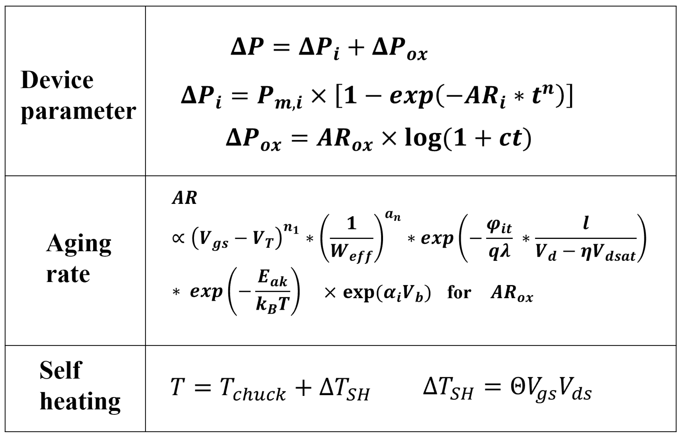
2. Compact Model and Physics
2.1. Reaction–Diffusion Framework
2.2. Discussion on Aging Rate (AR)
2.3. Discussion on Oxide Traps and Substrate Voltage
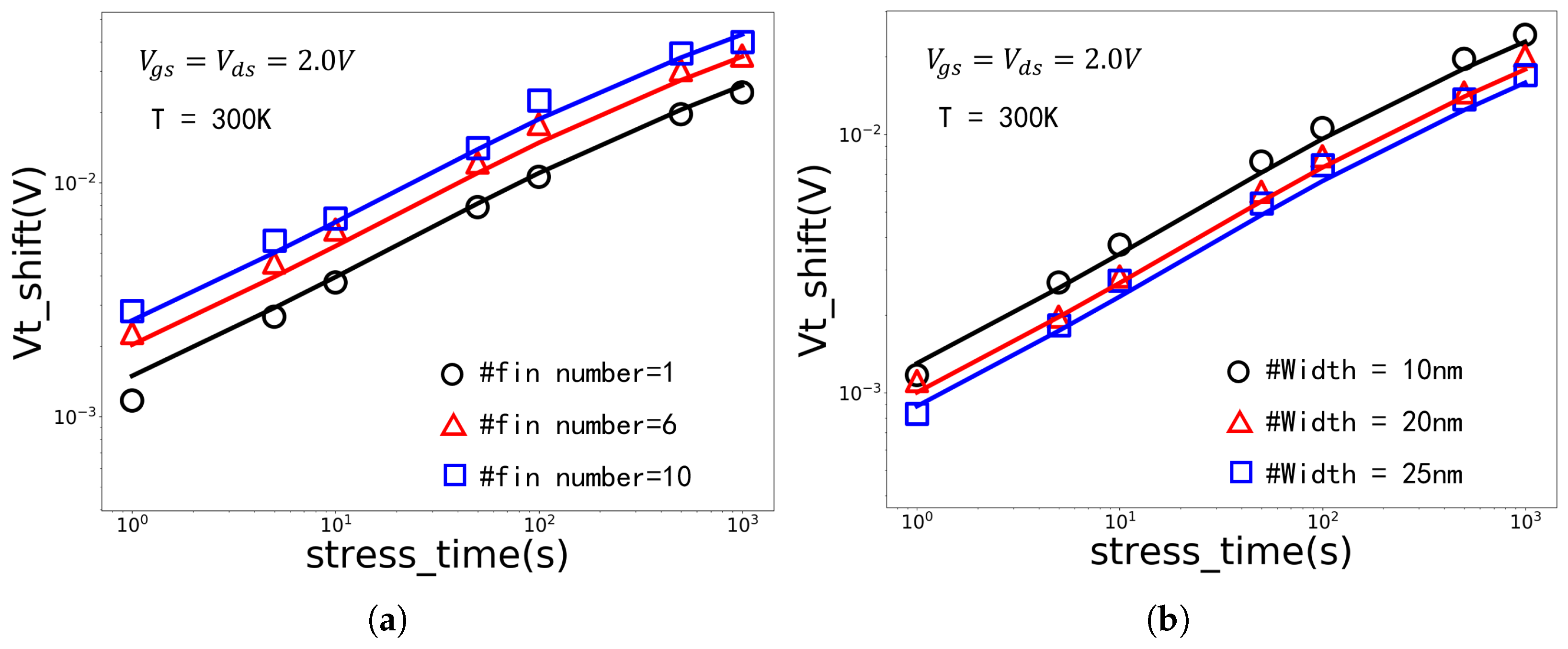
2.4. Discussion on Fin Width
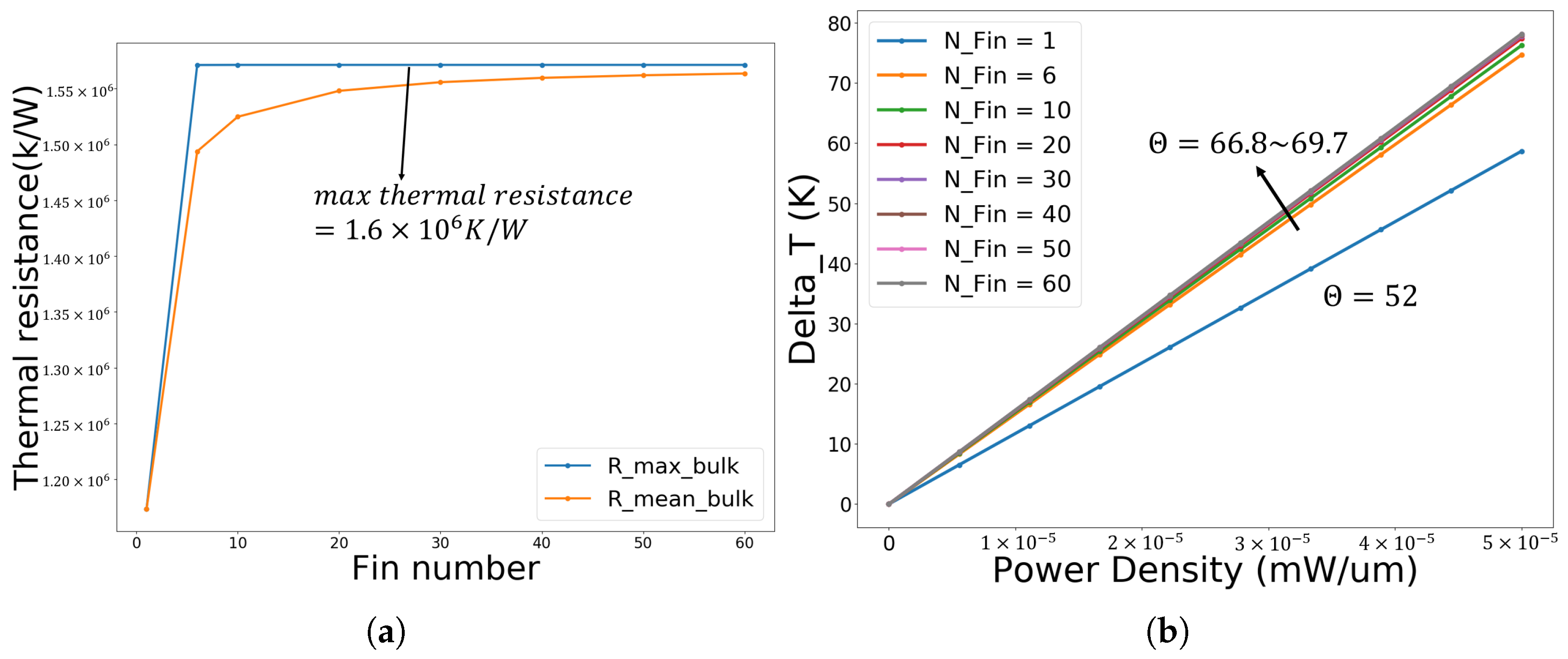
2.5. Coupling Effects of Self-Heating
3. Results and Discussion
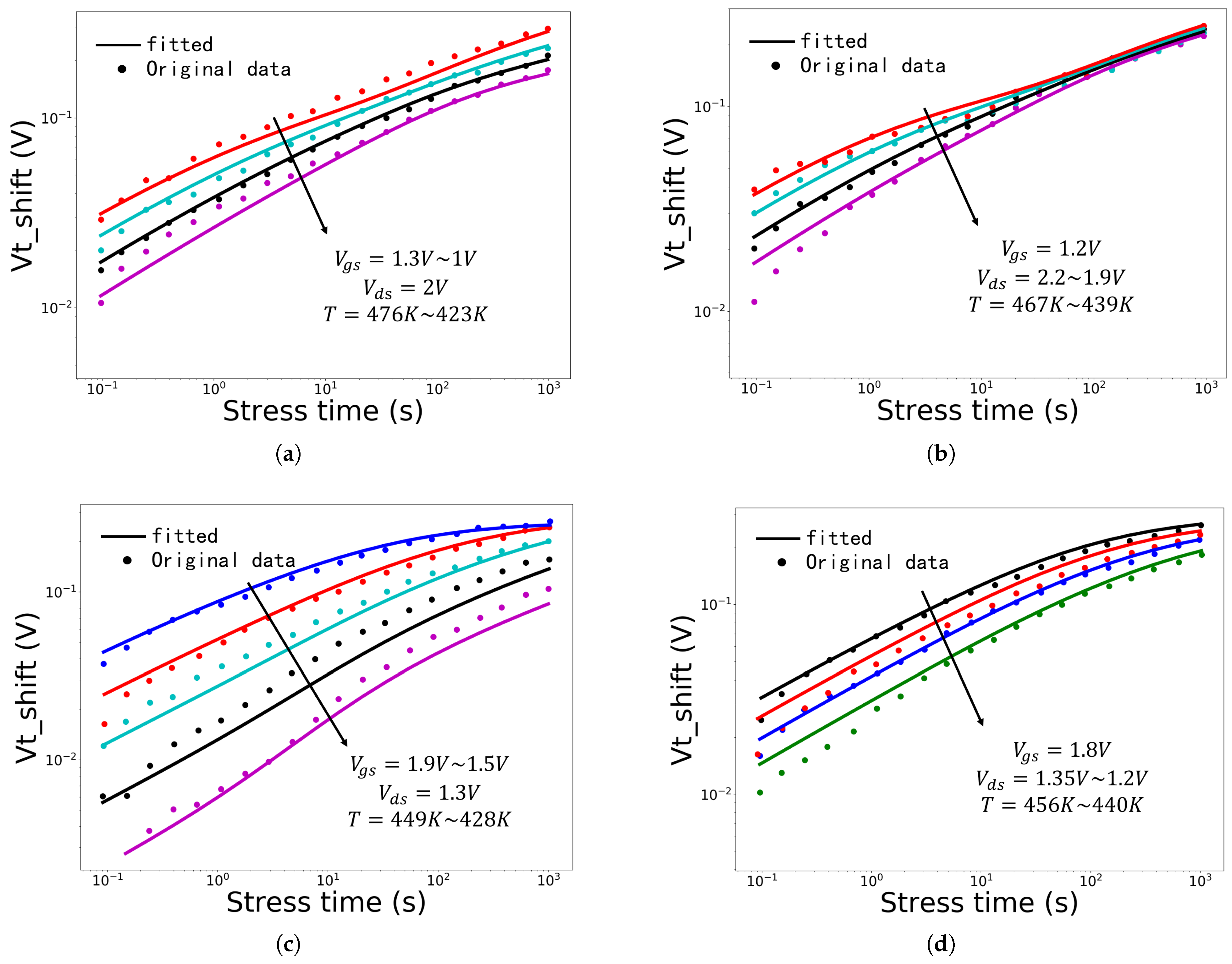
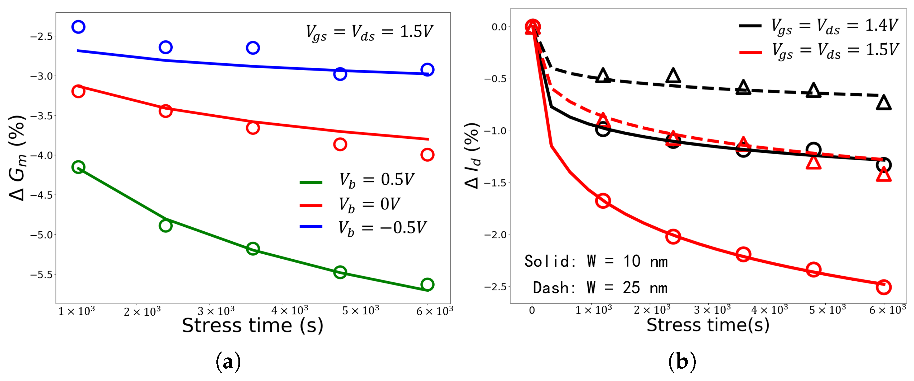
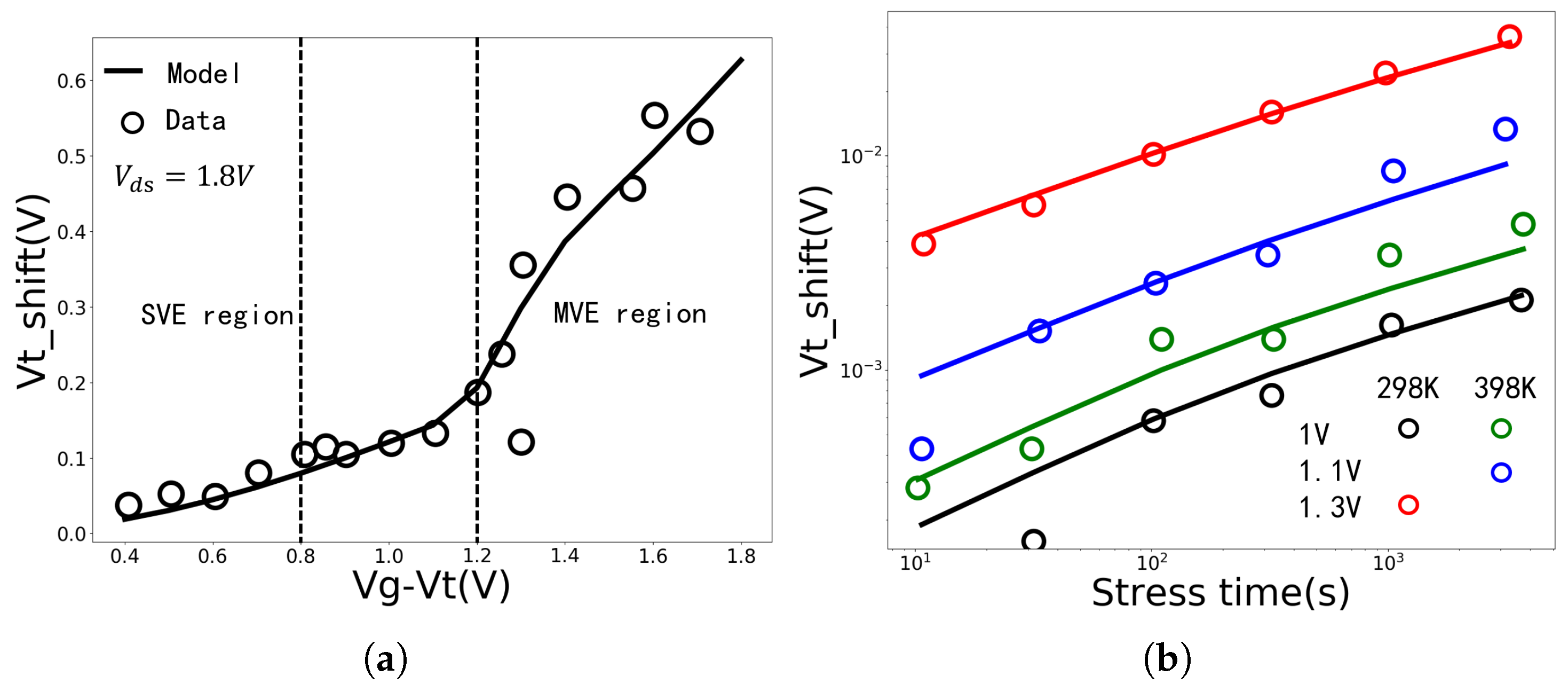
3.1. Model Parameter Fitting
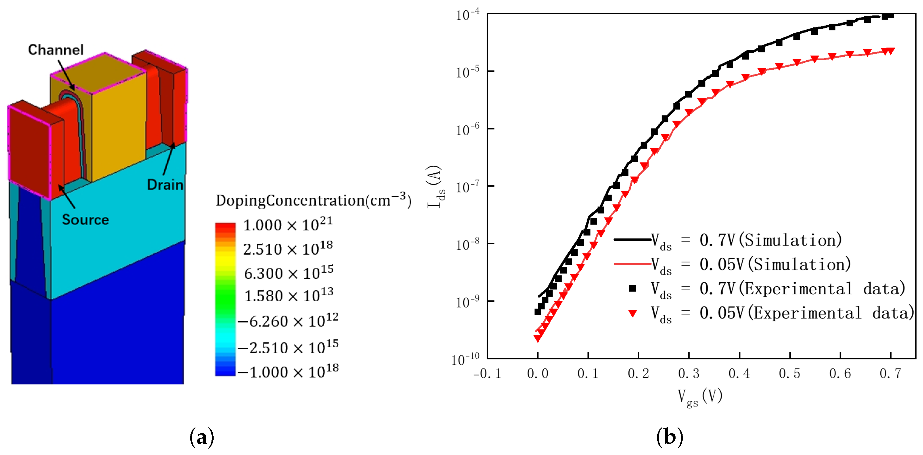
3.2. Model Validation Using TCAD Data
4. Conclusions
Author Contributions
Funding
Data Availability Statement
Conflicts of Interest
References
- Reddy, M.N.; Panda, D.K. A Comprehensive Review on FinFET in Terms of Its Device Structure and Performance Matrices. Silicon 2022, 10, 142–149. [Google Scholar] [CrossRef]
- Huard, V.; Parthasarathy, C.; Bravaix, A.; Guerin, C.; Pion, E. CMOS Device Design-in Reliability Approach in Advanced Nodes. In Proceedings of the 2009 IEEE International Reliability Physics Symposium, Montreal, QC, Canada, 26–30 April 2009. [Google Scholar] [CrossRef]
- Hu, C.; Tam, S.C.; Hsu, F.; Ko, P.; Chan, T.; Terrill, K.W. Hot-Electron-Induced MOSFET Degradation—Model, Monitor, and Improvement. IEEE J. Solid-State Circuits 1985, 20, 295–305. [Google Scholar] [CrossRef]
- Mcmahon, W.; Hess, K. A Multi-Carrier Model for Interface Trap Generation. J. Comput. Electron. 2002, 1, 395–398. [Google Scholar] [CrossRef]
- Rauch, S.E.; La Rosa, G. The Energy-Driven Paradigm of NMOSFET Hot-Carrier Effects. IEEE Trans. Device Mater. Reliab. 2005, 5, 701–705. [Google Scholar] [CrossRef]
- Bravaix, A.; Guerin, C.; Huard, V.; Roy, D.; Roux, J.M.; Vincent, E. Hot-Carrier Acceleration Factors for Low Power Management in DC-AC Stressed 40nm NMOS Node at High Temperature. In Proceedings of the 2009 IEEE International Reliability Physics Symposium, Montreal, QC, Canada, 26–30 April 2009. [Google Scholar] [CrossRef]
- Cacho, F.; Arfaoui, W.; Mora, P.; Federspiel, X.; Huard, V.; Dornel, E. Modeling of Hot Carrier Injection across Technology Scaling. In Proceedings of the 2014 IEEE International Integrated Reliability Workshop Final Report, South Lake Tahoe, CA, USA, 12–16 October 2014. [Google Scholar] [CrossRef]
- Reggiani, S.; Barone, G.; Poli, S.; Gnani, E.; Gnudi, A.; Baccarani, G.; Chuang, M.-Y.; Tian, W.; Wise, R. TCAD Simulation of Hot-Carrier and Thermal Degradation in STI-LDMOS Transistors. IEEE Trans. Electron Devices 2013, 60, 691–698. [Google Scholar] [CrossRef]
- Penzin, O.; Haggag, A.; McMahon, W.; Lyumkis, E.; Hess, K. MOSFET Degradation Kinetics and Its Simulation. IEEE Trans. Electron Devices 2003, 50, 1445–1450. [Google Scholar] [CrossRef]
- Lee, Y.-H.; Liao, P.J.; Joshi, K.; Huang, D.S. Circuit-Based Reliability Consideration in FinFET Technology. In Proceedings of the 2017 IEEE 24th International Symposium on the Physical and Failure Analysis of Integrated Circuits, Chengdu, China, 4–7 July 2017. [Google Scholar] [CrossRef]
- Qu, T.; Lin, X.; Li, J.K.; Cheng, R.; Yu, X.; Zheng, Z.J.; Lu, J.W.; Chen, B.; Zhao, Y. Ultra fast (<1 ns) electrical characterization of self-heating effect and its impact on hot carrier injection in 14 nm FinFETs. In Proceedings of the 2017 IEEE International Electron Devices Meeting, San Francisco, CA, USA, 2–6 December 2017. [Google Scholar] [CrossRef]
- Takeda, E.; Suzuki, N. An Empirical Model for Device Degradation Due to Hot-Carrier Injection. IEEE Electron Device Lett. 1983, 4, 111–113. [Google Scholar] [CrossRef]
- Ghobadi, N.; Afzali-Kusha, A.; Asl-Soleimani, E. Analytical Modeling of Hot Carrier Injection Induced Degradation in Triple Gate Bulk FinFETs. In Proceedings of the 2009 1st Asia Symposium on Quality Electronic Design Meeting, Kuala Lumpur, Malaysia, 15–16 July 2009. [Google Scholar] [CrossRef]
- Sharma, U.; Mahapatra, S. A SPICE Compatible Compact Model for Hot-Carrier Degradation in MOSFETs Under Different Experimental Conditions. IEEE Trans. Electron Devices 2019, 66, 839–846. [Google Scholar] [CrossRef]
- Ji, Z.; Chen, H.; Li, X. Design for Reliability with the Advanced Integrated Circuit (IC) Technology: Challenges and Opportunities. Sci. China Inf. Sci. 2019, 62, 226401. [Google Scholar] [CrossRef]
- Chang, W.-T.; Cin, L.-G.; Yeh, W.-K. Impact of Fin Width and Back Bias Under Hot Carrier Injection on Double-Gate FinFETs. IEEE Trans. Device Mater. Relib 2015, 15, 86–89. [Google Scholar] [CrossRef]
- Yu, Z.; Zhang, J.; Wang, R.; Guo, S.; Liu, C.; Huang, R. New Insights into the Hot Carrier Degradation (HCD) in FinFET: New Observations, Unified Compact Model, and Impacts on Circuit Reliability. In Proceedings of the 2017 IEEE International Electron Devices Meeting, San Francisco, CA, USA, 2–6 December 2017. [Google Scholar] [CrossRef]
- Sriram, S.R.; Bindu, B. Analytical Model of Hot Carrier Degradation in Uniaxial Strained Triple-Gate FinFET for Circuit Simulation. J. Comput. Electron. 2018, 17, 163–171. [Google Scholar] [CrossRef]
- Wang, W.; Reddy, V.; Krishnan, A.T.; Vattikonda, R.; Krishnan, S.; Cao, Y. Compact Modeling and Simulation of Circuit Reliability for 65-Nm CMOS Technology. IEEE Trans. Device Mater. 2007, 7, 509–517. [Google Scholar] [CrossRef]
- Wang, R.; Sun, Z.; Liu, Y.-Y.; Yu, Z.; Wang, Z.; Jiang, X.; Huang, R. Understanding Hot Carrier Reliability in FinFET Technology from Trap-Based Approach. In Proceedings of the 2021 IEEE International Electron Devices Meeting, San Francisco, CA, USA, 11–16 December 2021. [Google Scholar] [CrossRef]
- Ishigaki, T.; Tsuchiya, R.; Morita, Y.; Sugii, N.; Kimura, S. Effects of Device Structure and Back Biasing on HCI and NBTI in Silicon-on-Thin-BOX (SOTB) CMOSFET. IEEE Trans. Electron Devices 2011, 58, 1197–1204. [Google Scholar] [CrossRef]
- Jiang, H.; Shin, S.; Liu, X.; Zhang, X.; Alam, M.A. The Impact of Self-Heating on HCI Reliability in High-Performance Digital Circuits. IEEE Electron Device Lett. 2017, 38, 430–433. [Google Scholar] [CrossRef]
- Jiang, H.; Shin, S.; Liu, X.; Zhang, X.; Alam, M.A. Characterization of Self-Heating Leads to Universal Scaling of HCI Degradation of Multi-Fin SOI FinFETs. In Proceedings of the 2016 IEEE International Reliability Physics Symposium, Pasadena, CA, USA, 17–21 April 2016. [Google Scholar] [CrossRef]
- Xu, C.; Kolluri, S.K.; Endo, K.; Banerjee, K. Analytical Thermal Model for Self-Heating in Advanced FinFET Devices with Implications for Design and Reliability. IEEE Trans. Comput.-Aided Des. Integr. Circuits Syst. 2013, 32, 1045–1058. [Google Scholar] [CrossRef]
- Ciou, F.-M.; Lin, J.-H.; Chen, P.-H.; Chang, T.-C.; Chang, K.-C.; Hsu, J.-T.; Lin, Y.-S.; Jin, F.-Y.; Hung, W.-C.; Yeh, C.-H.; et al. Comparison of the Hot Carrier Degradation of N- and P-Type Fin Field-Effect Transistors in 14-Nm Technology Nodes. IEEE Electron Device Lett. 2021, 42, 1420–1423. [Google Scholar] [CrossRef]
- Natarajan, S.; Agostinelli, M.; Akbar, S.; Bost, M.; Bowonder, A.; Chikarmane, V.; Chouksey, S.; Dasgupta, A.; Fischer, K.; Fu, Q.; et al. A 14 nm logic technology featuring 2nd-generation finfet, air-gapped interconnects, self-aligned double patterning and a 0.0588 µm2 sram cell size. In Proceedings of the 2014 IEEE International Electron Devices Meeting, San Francisco, CA, USA, 15–17 December 2014. [Google Scholar] [CrossRef]


| Fin Width (nm) | Fin Height (nm) | Channel Length (nm) |
|---|---|---|
| 10 | 30 | 20 |
| Channel (W/m·K) | Source/Drain (W/m·K) | Gate Oxide SiO2 (W/m·K) |
|---|---|---|
| 14 | 62 | 1.4 |
| Parameters | SVE Region | MVE Region |
|---|---|---|
| n | 0.38324 | 0.3422 |
| c () | 0.02505 | 0.1344 |
| 2.99 | 11.907 | |
| 1.889 | 2.082 | |
| 7.545 | 2.38693 | |
| 0.6403 | 3.76661 | |
| 0.076 | 0.076 | |
| Lifetime Under HC Stress (2 V) | V | V | |
|---|---|---|---|
| TCAD data | s | s | s |
| Compact model | s | s | s |
| Compact Model | Traditional Model | Lifetime Obtained from [11] | |
|---|---|---|---|
| Lifetime under working condition (0.74 V) |
Disclaimer/Publisher’s Note: The statements, opinions and data contained in all publications are solely those of the individual author(s) and contributor(s) and not of MDPI and/or the editor(s). MDPI and/or the editor(s) disclaim responsibility for any injury to people or property resulting from any ideas, methods, instructions or products referred to in the content. |
© 2025 by the authors. Licensee MDPI, Basel, Switzerland. This article is an open access article distributed under the terms and conditions of the Creative Commons Attribution (CC BY) license (https://creativecommons.org/licenses/by/4.0/).
Share and Cite
Liu, B.; Chen, L. Self-Heating Effect Coupled Compact Model to Predict Hot Carrier Injection Degradation in Nanoscale Bulk FinFETs Under Different Conditions. Appl. Sci. 2025, 15, 2351. https://doi.org/10.3390/app15052351
Liu B, Chen L. Self-Heating Effect Coupled Compact Model to Predict Hot Carrier Injection Degradation in Nanoscale Bulk FinFETs Under Different Conditions. Applied Sciences. 2025; 15(5):2351. https://doi.org/10.3390/app15052351
Chicago/Turabian StyleLiu, Bingrui, and Lan Chen. 2025. "Self-Heating Effect Coupled Compact Model to Predict Hot Carrier Injection Degradation in Nanoscale Bulk FinFETs Under Different Conditions" Applied Sciences 15, no. 5: 2351. https://doi.org/10.3390/app15052351
APA StyleLiu, B., & Chen, L. (2025). Self-Heating Effect Coupled Compact Model to Predict Hot Carrier Injection Degradation in Nanoscale Bulk FinFETs Under Different Conditions. Applied Sciences, 15(5), 2351. https://doi.org/10.3390/app15052351