Article

WRTU-16T: Write-Enhanced Low-Power Radiation-Tolerant SRAM for Space Applications

Department of Semiconductor Engineering, Tech University of Korea, Siheung 15073, Republic of Korea
*
Author to whom correspondence should be addressed.
Appl. Sci. 2025, 15(13), 7295; https://doi.org/10.3390/app15137295 (registering DOI)
Submission received: 21 May 2025 / Revised: 22 June 2025 / Accepted: 27 June 2025 / Published: 28 June 2025

Abstract

In space, high-energy particle radiation poses a serious threat to the data stability and reliability of SRAM. Existing radiation-tolerant techniques, such as Triple Modular Redundancy (TMR) and Error Correction Code (ECC), have disadvantages such as large area, high power consumption, and additional delay, making them unsuitable for small satellite systems. To overcome these limitations, this paper proposes a 16-transistor-based radiation-tolerant SRAM cell, WRTU-16T, which applies a read-decoupled structure and a charge-sharing suppression mechanism. The proposed structure effectively isolates the storage node from external disturbances and improves the recovery capability for single-event inversion (SEU) and multiple-node inversion (SEMNU) by reducing charge loss. WRTU-16T shows superior performance in terms of write delay, charge recovery capability (Qc), hold power, and word line write threshold voltage (WWTV) compared to existing radiation-tolerant SRAM designs. The integrated circuit is implemented using a 90 nm CMOS process and has an operating voltage of 1V.

1. Introduction

The advancement of integrated circuit technology has dramatically improved the performance of satellite communication systems, and as a result, its application scope is expanding in the space industry. Static random access memory (SRAM) is used as a core memory, from small satellites to large-scale satellite networks, due to its advantage of a high operation speed [1]. However, in space, high-energy particles continuously collide with memory cells, posing a great threat to the reliability of SRAM. Radiation-induced errors such as SEU (Single-Event Upset) or SEMNU (Single-Event Multiple Node Upset) can corrupt stored data or cause system malfunction. As the physical size of sensitive nodes decreases due to the continuous miniaturization of CMOS processes, SRAM is becoming more vulnerable to SEU.
Previously, methods such as TMR (Triple Modular Redundancy) or ECC (Error Correction Code) were used to alleviate these problems. However, these methods have the disadvantage of significantly increasing the area or power consumption or increasing the circuit delay, making them unsuitable for systems with limited cost or power budget. Therefore, the demand for more efficient and reliable radiation-hardened SRAM structures suitable for space environments is increasing. The We-Quatro [2] cell has two pairs of NMOS access transistors that connect directly to two storage nodes and two inner nodes. These features provide low Write Access Time (WAT) and Read Access Time (RAT) for fast operation. The primary issue with this design is the high Hold Power (HPWR) because of its short NMOS paths. The RRHS-14T [3] radiation-hardened cell has four NMOS access transistors and is designed with an optimized cell ratio (CR) of 2:1 for writing ability. The design’s best feature is its highest WAT and Word Line Write Trip Voltage (WWTV) while exhibiting the lowest critical charge (Qc) among comparison cells. And also, the lack of internal feedback paths fails to restore data in radiation environments. The RHSCC-16T [4] is unique in that it has two storage nodes and four inner nodes. When one of the six nodes is affected by SEU or SEMNU, it can be restored to the correct logic value through the feedback loop structure of the unaffected node. The use of feedback RHSCC-16T achieves high Qc. As a trade-off, those complex structures cause additional circuit latency, leading to high WAT and RAT. A 16T radiation-hardened SRAM with eight NMOSs and eight PMOSs, SUR-16T [5], incorporates two PMOS access transistors influencing transistor stacking to reduce the HPWR. However, this cell operates with excessive delays with high WAT and RAT, as well as a small Read Static Noise Margin (RSNM) because of PMOS access devices. The structure of S8P8N-16T [6] has four access transistors, two PMOSs connecting inner nodes, and two NMOSs related to storage nodes. S8P8N-16T has a low HPWR by using relatively more PMOSs than other cells for the stacking effect. Additionally, inner nodes are surrounded by NMOS, and storage nodes are surrounded by PMOSs for low WAT and high WWTV. However, one pair of PMOSs creates the parasitic capacitance reason for low RSNM.
Although several radiation-hardened SRAM cells have been proposed recently, many of them are effective only under certain conditions or do not properly balance read stability, write latency, and power consumption. Some cells are robust to single-node errors, but are still vulnerable to multi-node inversions or have excessively high leakage power. In this paper, we propose a radiation-hardened SRAM cell, WRTU-16T, to overcome these limitations. This structure combines a ‘read separation’ structure that separates read operations from storage nodes and a ‘charge-sharing suppression’ technique that suppresses the phenomenon of charges being distributed across multiple nodes. This isolates the storage nodes from the direct effects of radiation, reduces the possibility of SEMNU occurrence, and enables the structure to recover quickly even when SEU occurs. In addition, it achieves high write stability, short write latency, and low hold power consumption. In this paper, the structural characteristics and design methodology of the WRTU-16T cell are detailed in Section 2, while performance comparisons with the conventional cells are presented in Section 3.

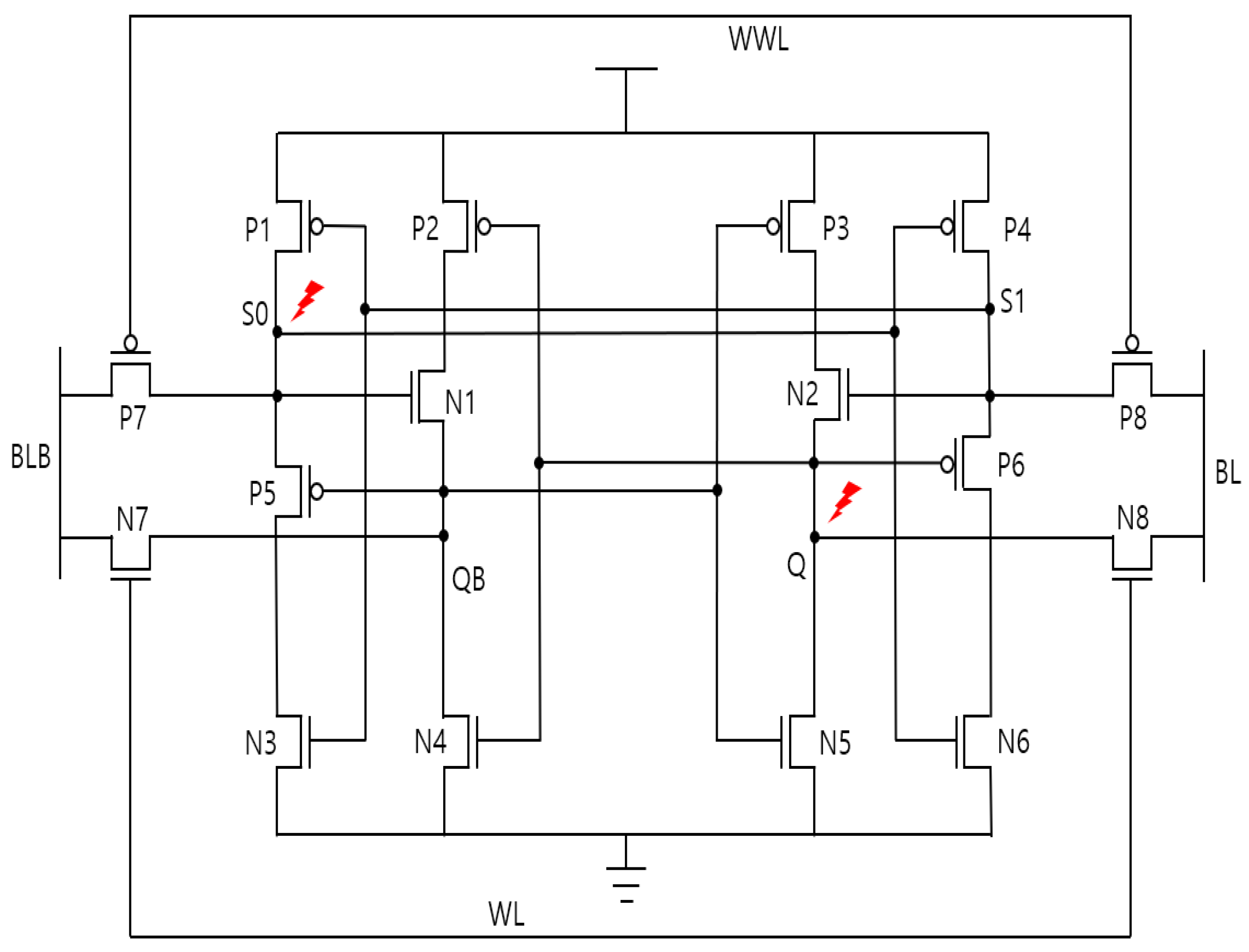
2. Proposed WRTU-16T SRAM Architecture

2.1. Proposed Cell Design
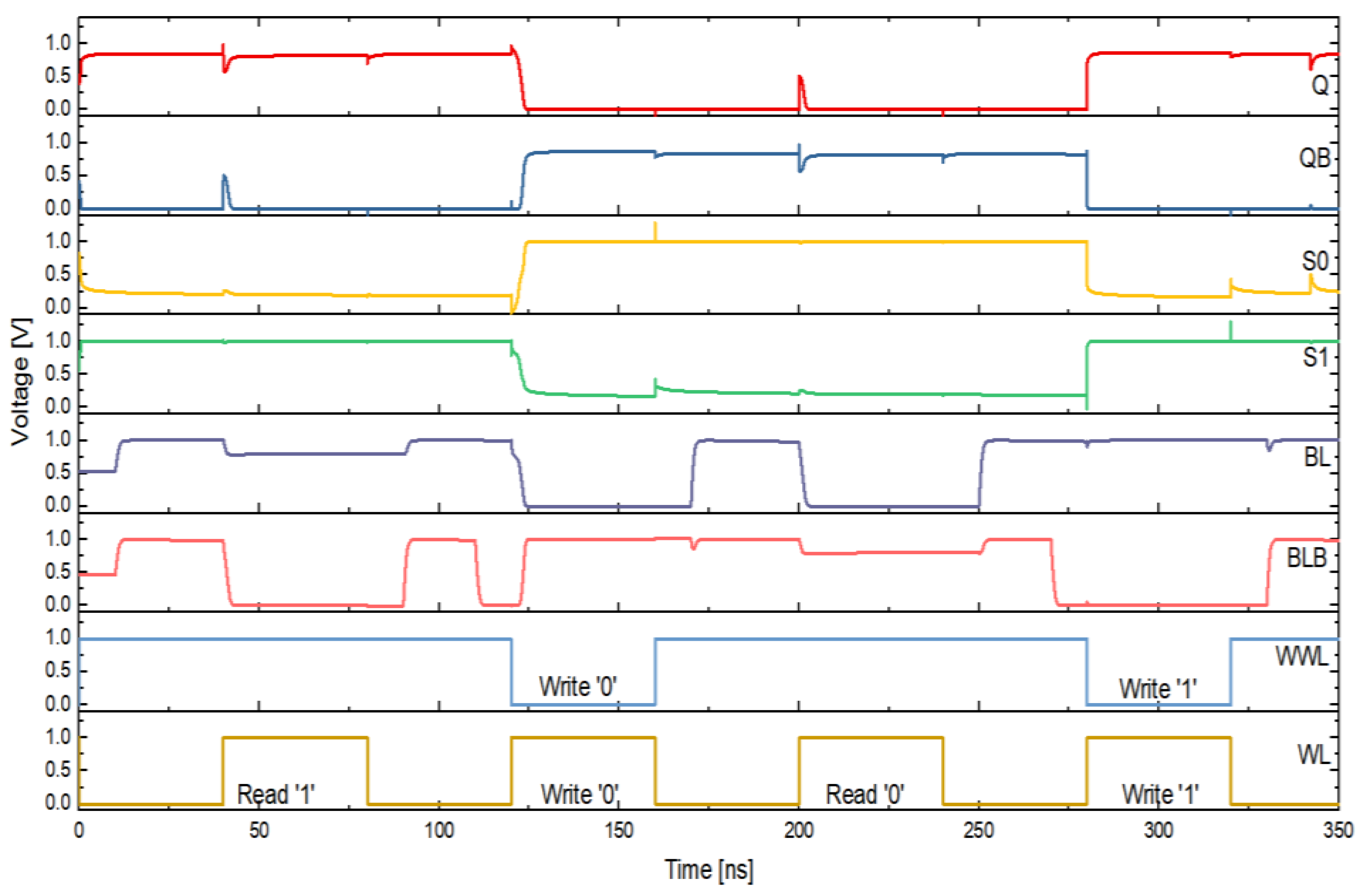
The schematic and layout of the WRTU-16T cell are presented in Figure 1 and Figure 2. The proposed WRTU-16T cell is composed of 16 transistors and incorporates two storage nodes (Q, QB) and two internal nodes (S0, S1). Both the SEU recovery capability and write performance are enhanced by the 16-transistor architecture through three design features: dual feedback paths between the storage and internal nodes, the physical isolation of sensitive nodes, and an access structure that employs both PMOS and NMOS transistors. The four access transistors are implemented using one pair of PMOS and one pair of NMOS transistors [7]. Only two pairs of nodes are considered critical in terms of SEU susceptibility, thereby enhancing recovery capability [8]. Transistor sizing is configured as follows: P1, P2, P3, and P4 are each assigned a width-to-length (W/L) ratio of 3; P7 and P8 are each assigned a ratio of 9; and N7 and N8 are each assigned a ratio of 3. All other transistors are designed with the minimum feature sizes allowed by the process design rules. These sizing decisions are implemented to strengthen immunity against SNUs, improving write performance and power efficiency. Read operations are performed through two access transistors, N7 and N8, while write operations are executed using all four access transistors, N7, N8, P7, and P8. When a logic ‘1’ is stored, the node states are established as Q = S1 = 1 and QB = S0 = 0.

2.2. Hold Operation

During the hold state, when the cell stores logic ‘1’ (Q = S1 = 0, QB = S0 = 1), no read or write access is performed during hold. WL is held LOW and WWL is held HIGH so that P7, P8, N7, and N8 remain deactivated. As a result, the storage nodes are isolated from bit lines, and cross-coupled inverters retain the data.

2.3. Write Operation

During the write state, when transitioning logic from ‘0’ to ‘1’ (Q = S1 = 1, QB = S0 = 0), BL is driven to VDD and BLB is driven to VSS so that P7, P8, N7, and N8 are activated. Q is pulled from 0 to 1 through N8 and QB is pulled from 1 to 0 through N7. Simultaneously, S1 is driven from 0 to 1 through P8 and S0 is driven from 1 to 0 through P7. As a result, the storage and internal nodes are switched in coordination [9].

2.4. Read Operation

During the read state, when the cell stores logic ‘1’ (Q = S1 = 1, QB = S0 = 0), BL and BLB are pre-charged to VDD, and WL and WWL are then asserted as HIGH, turning on transistors N7 and N8 to connect the internal nodes to the bit lines. BL remains at VDD through N8 and BLB discharges through N7, producing a voltage differential (ΔV > 50 mV). As a result, the sense amplifier is triggered by the differential and the stored data is output. During read, storage nodes remain undisturbed so that the original data is preserved. Operational waveforms of WRTU-16T during the hold, read, and write modes are identified in Figure 3.

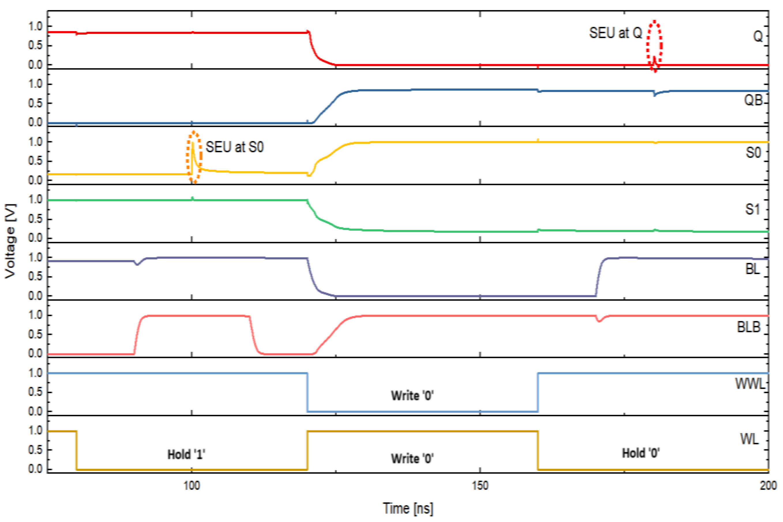
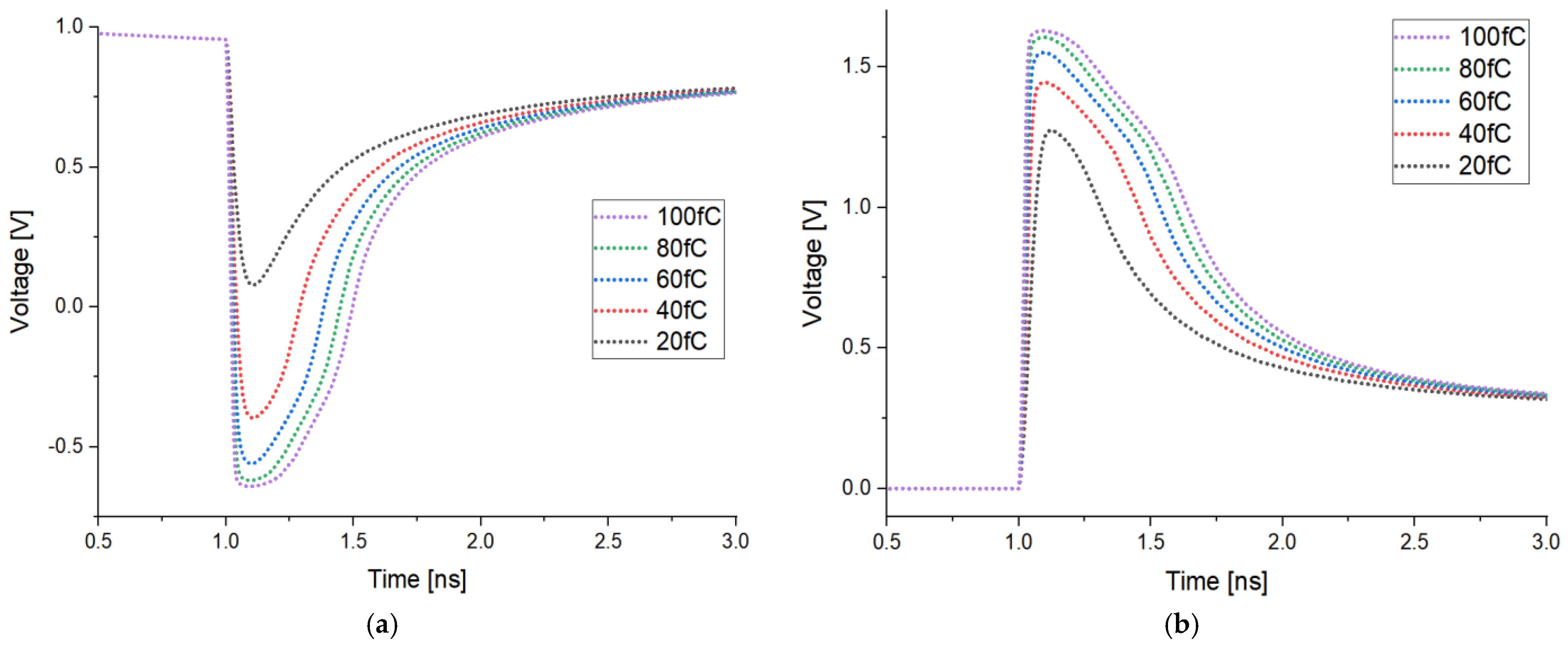
2.5. SEU Recovery Analysis

The recovery analysis is described based on the assumption that the cell is storing a logic ‘1’. Two internal nodes and two storage nodes exist in WRTU-16T, and only two nodes—Q and S0—are considered sensitive to SEU. Therefore, two single-node upset scenarios (at Q and at S0) and one simultaneous multiple-node upset case, in which recovery from radiation-induced upsets is enabled by inherent electrical feedback and circuit structure, are examined.

2.5.1. SEU at Node Q

An SEU at node Q causes a transient flip from logic ‘1’ to logic ‘0’; transistor N4 turned OFF, and, in contrast, P2 and P6 turned ON. Consequently, the QB value becomes high impedance, but the values stored at other nodes remain unaffected. The Q node is restored from logic ‘0’ to logic ‘1’ by the activation of P3 and N2.

2.5.2. SEU at Node S0

When node S0 is affected by SEU, the logic state of node S0 changes from “0” to “1”, which makes transistor P4 turn into temporary off and transistor N6 and N1 turn into temporary on. All nodes retain their logic values, but only the S1 node becomes high impedance. As a result, the S0 node is restored from logic ‘1’ to logic ‘0’ by activated P5 and N3. The SEU recovery operation is shown in Figure 4.

2.5.3. SEMNU at Node Pair Q-S0

A SEMNU at nodes Q and S0 causes a permanent flip from logic ‘1’ to logic ‘0’. In this case, all sensitive nodes are affected at once, and the recovery mechanism fails to restore the original data. To mitigate such events, a layout-level solution is required. Specifically, increasing the physical distance between nodes Q and S0 during the layout design can reduce the possibility of a simultaneous strike.

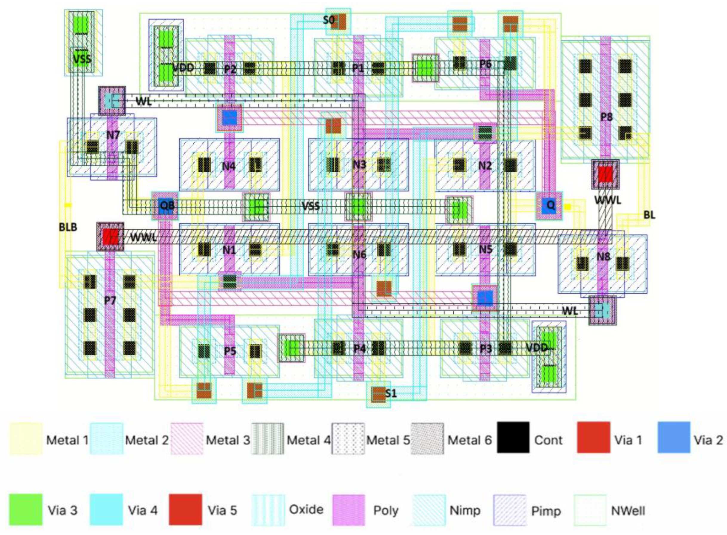
3. Implementation Results and Analysis

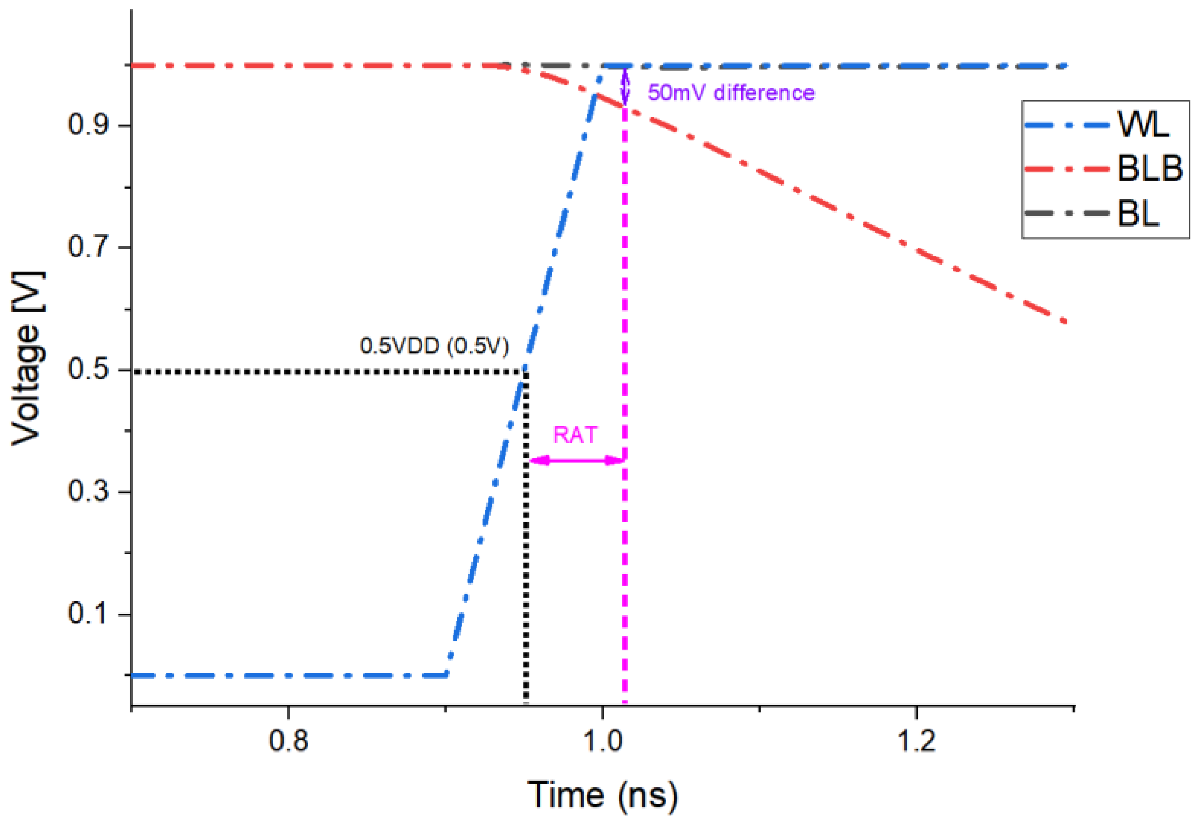
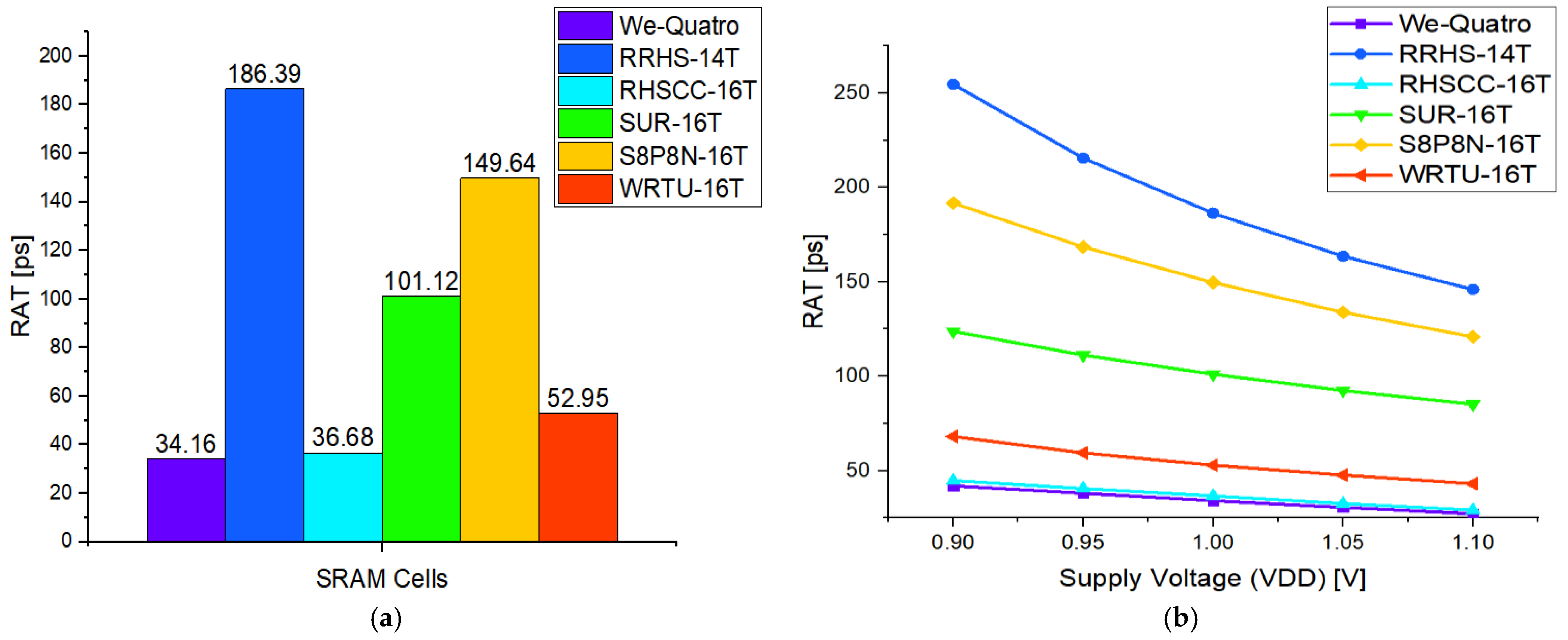
3.1. Read Access Time

The RAT is defined as the interval between the activation of the WL and the establishment of a specified voltage difference (e.g., 50 mV) between the BL and the BLB. The RAT is illustrated in Figure 5. The RAT is influenced by several circuit-level parameters, among which the read current through the access transistor and the pull-down transistor is dominant. A higher CR, defined as the ratio of the pull-down transistor strength to that of the access transistor, results in a stronger pull-down strength. The more rapid discharge of the bit line voltage is enabled, thus reducing the RAT. In contrast, an increased number of access transistors or the inclusion of PMOS transistors in the read path can lead to a higher bit line capacitance and voltage division effects, which may introduce additional read delay. As shown in Figure 6, the WRTU-16T achieves a fast read performance that incorporates electrically optimized PMOS/NMOS hybrid access transistors and a dedicated read-decoupled structure, which is isolated from the bit lines. The RAT of WRTU-16T is 52.95 ps, which is faster than the other SRAMs.

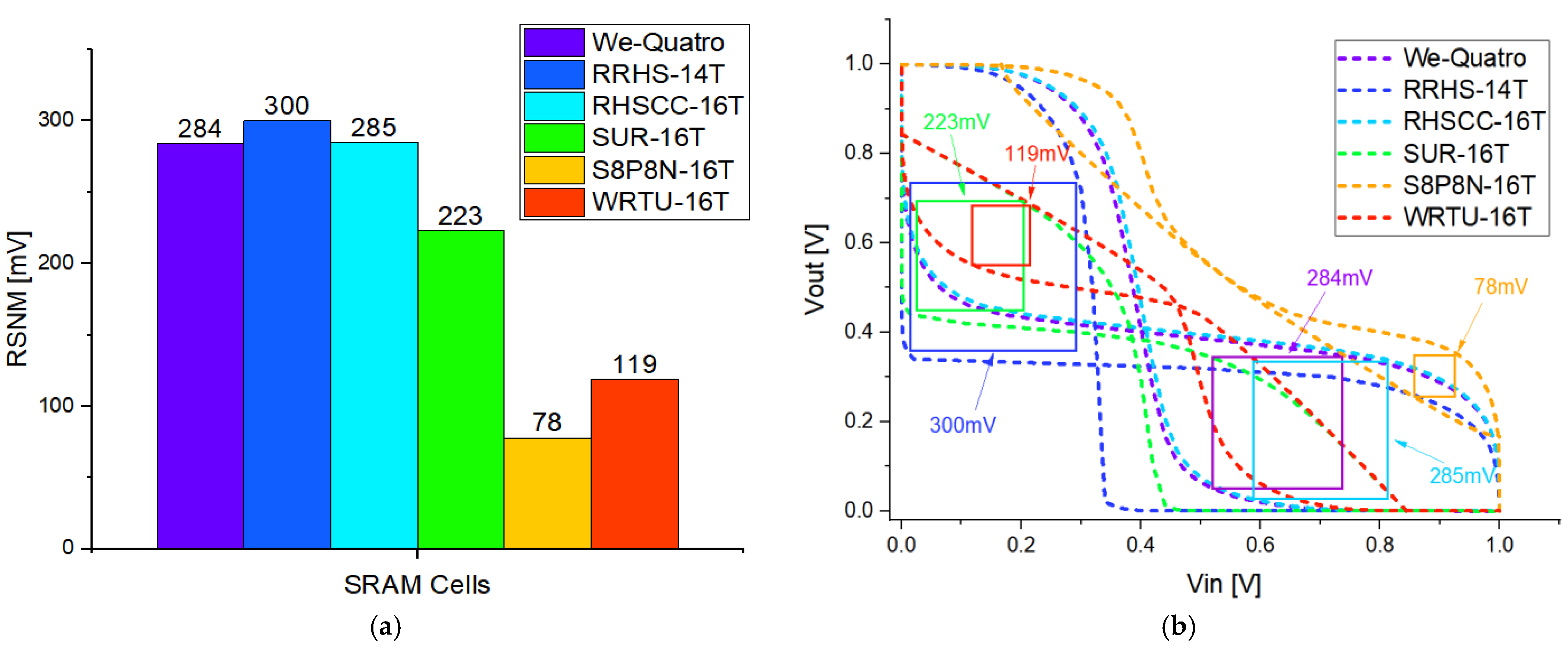
3.2. Read Static Noise Margin

The RSNM is defined as the maximum tolerance of an SRAM to external noise or bit line disturbances during a read operation, despite the presence of external noise or bit line disturbances. It is measured as the area of the largest square that can fit within the butterfly curve obtained by sweeping a DC voltage at the storage node. A higher RSNM value affect stronger immunity to soft errors and greater stability under noise-sensitive or radiation-exposed environments [10]. The RSNM is influenced by the implementation of read isolation structures, which enhances read stability by decoupling the storage node from direct interaction with the bit line during read operations. This prevents the read current from disturbing the storage node voltage. Other influencing factors include the number of access transistors, parasitic capacitances, transistor dimensions (W/L ratios), and the CR. As shown in Figure 7, the WRTU-16T shows a RSNM of 119 mV.

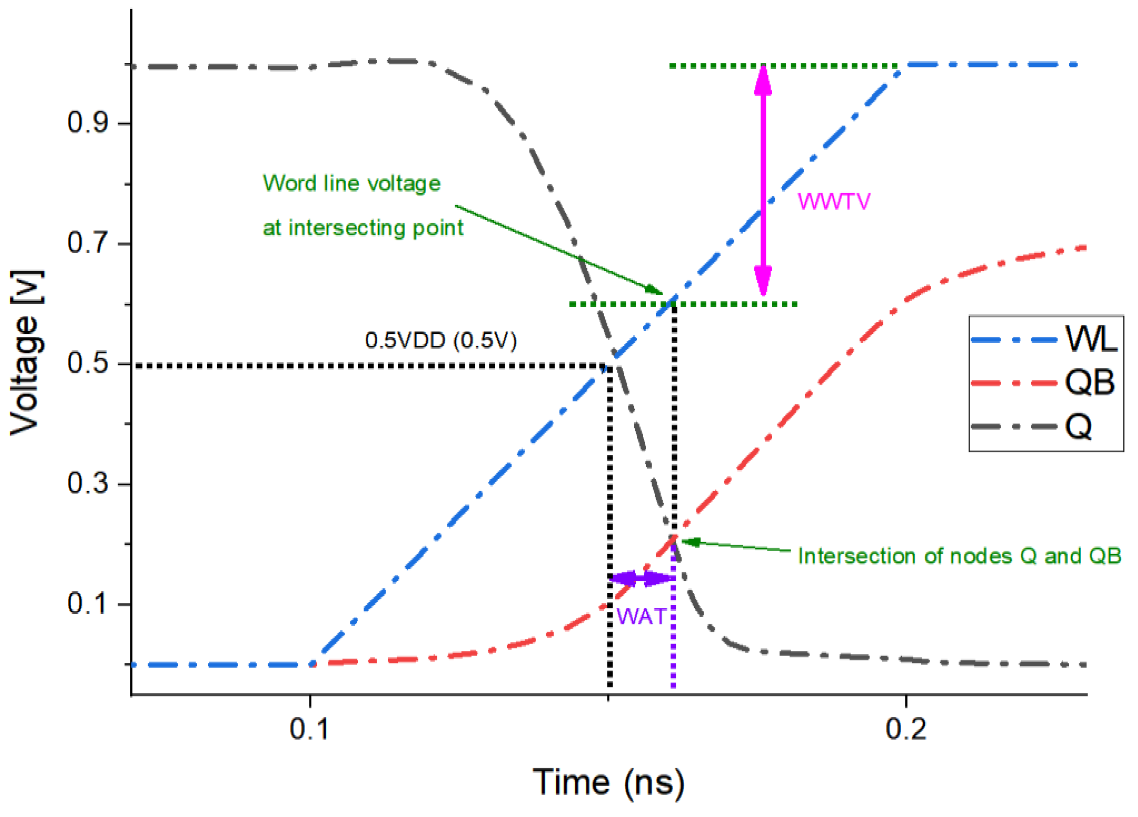
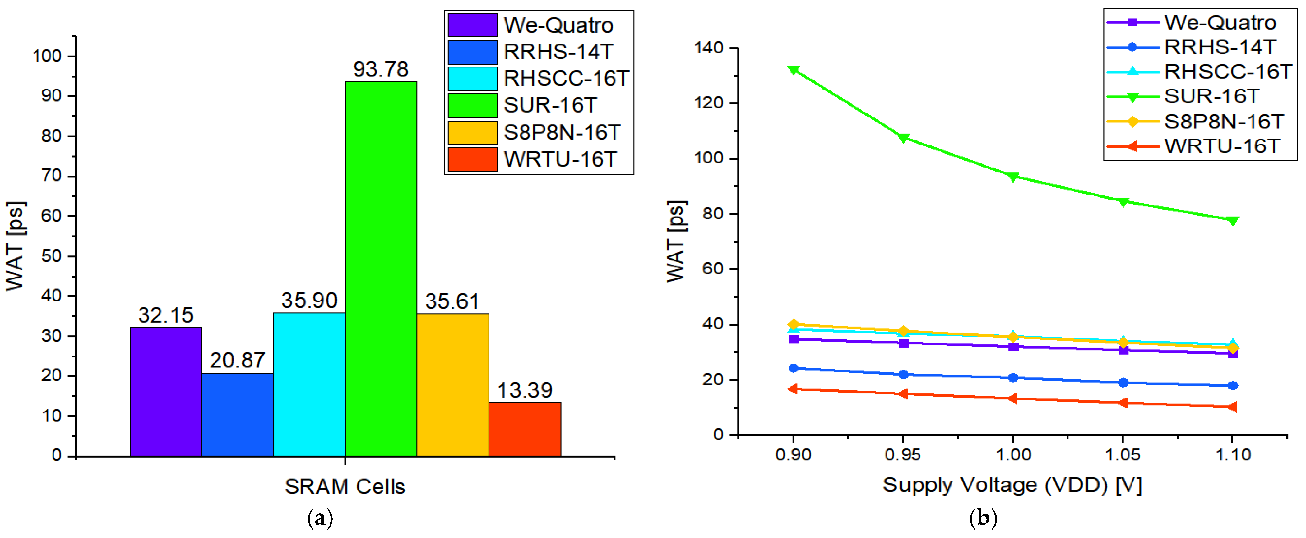
3.3. Write Access Time

The WAT is defined as the time interval between the moment the WL voltage reaches 50% of its full swing and the point at which the voltages of the storage node and its complementary node intersect. A shorter WAT means a faster write operation. Figure 8 shows the WAT and WWTV. The WAT is primarily influenced by the internal feedback structure, the number and type of access transistors, and the ease with which stored charges can be flipped during a write operation. First, WRTU-16T has a cross-coupled inverter pair that forms a feedback loop, accelerating the state transition by reinforcing voltage changes between Q and QB. Second, WRTU-16T has four access transistors—two PMOSs and two NMOSs—that simultaneously connect the storage nodes and internal nodes to the bit lines. This parallel access provides multiple discharge paths, enhancing the speed of write operations. Third, the storage nodes are surrounded by NMOS transistors, which tend to weakly hold a logic ‘1’, allowing for faster discharge through the bit lines during a write, thereby further reducing the WAT. The three architectural advantages reduce the unnecessary contending current and enable fast and reliable write performance. As shown in Figure 9, the WRTU-16T exhibits an improved WAT.

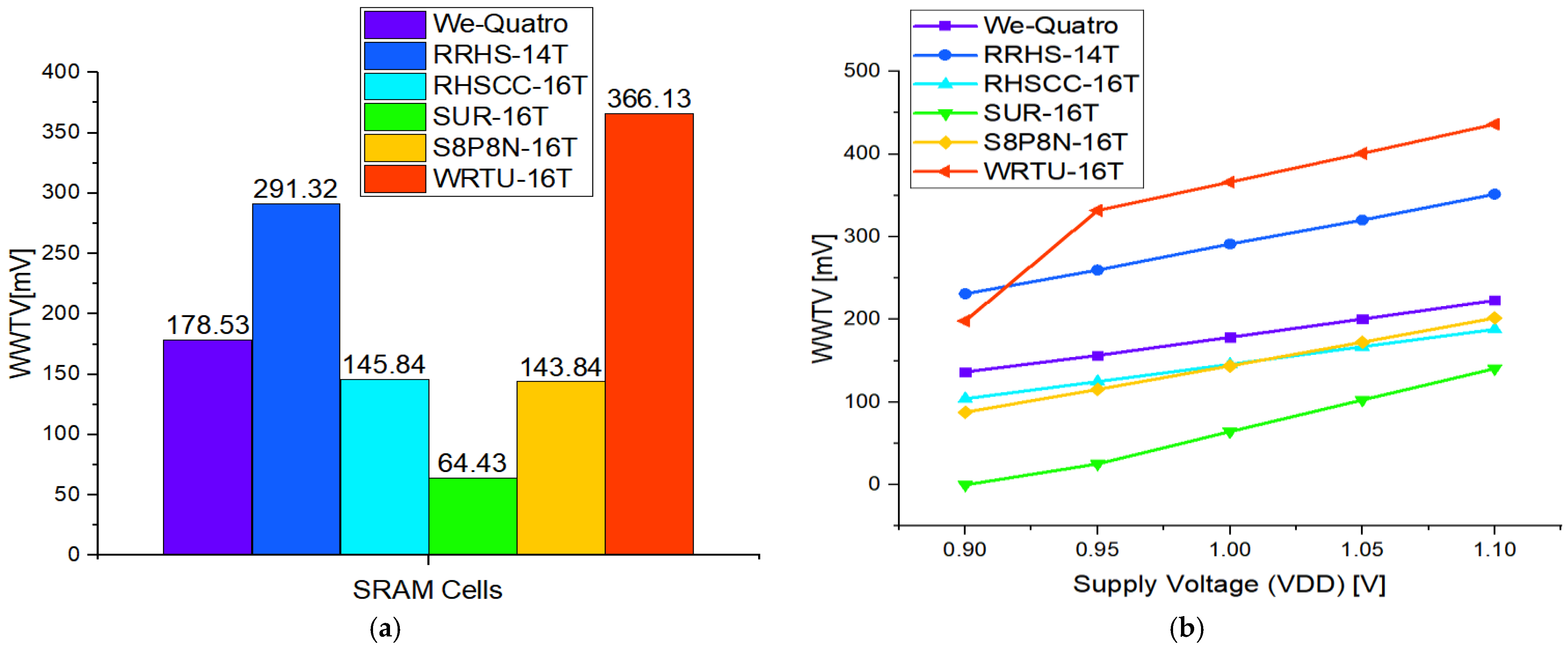
3.4. Word Line Write Trip Voltage
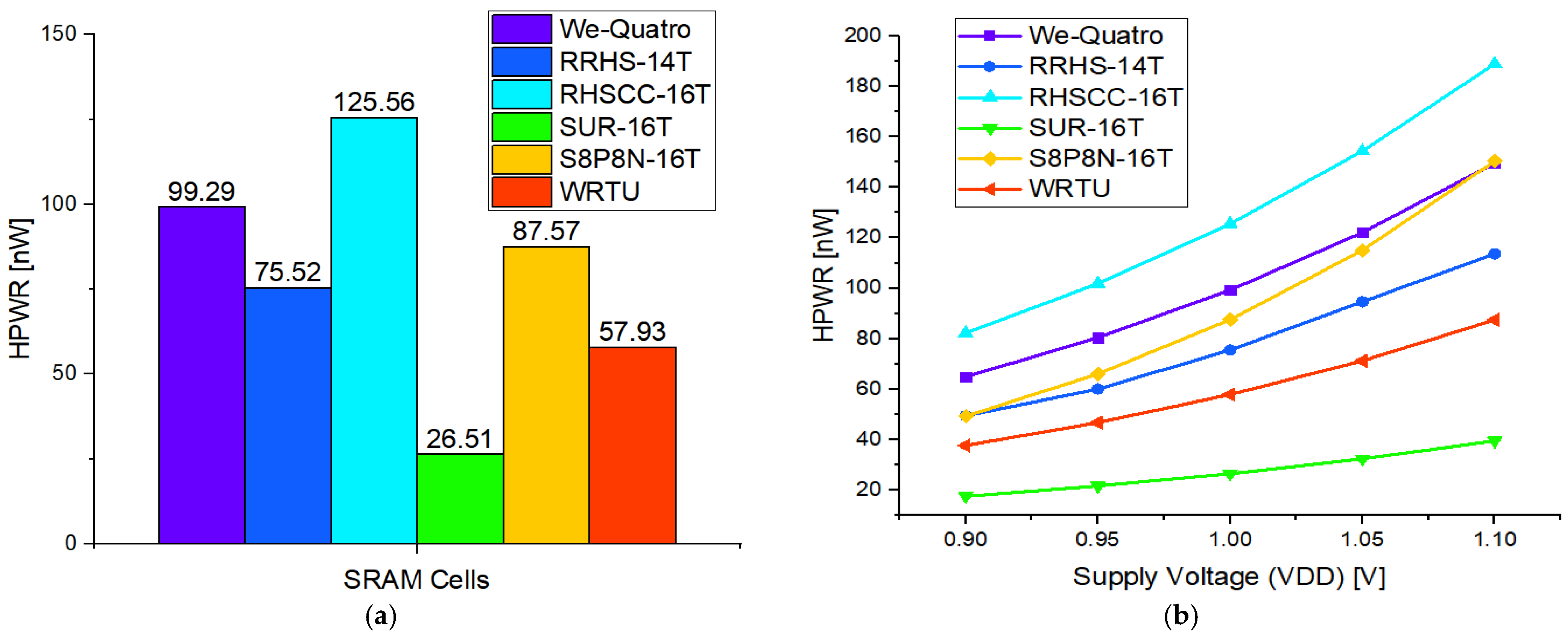
The WWTV means the voltage difference between the supply voltage and the word line voltage at the point where the voltages of the two storage nodes cross during a write operation. This metric is the minimum WL driving condition required to stably invert data, and is used as a quantitative measure to evaluate the write stability of SRAMs. Traditionally, the write static noise margin (WSNM) has been used to evaluate the write robustness, but recent studies have emphasized that the WWTV is a more practical metric because it directly reflects the dynamic write conditions [11]. The WWTV is closely correlated with the WAT. In general, SRAMs with a short WAT have a faster voltage inversion of the storage node, so they can write stably even under a lower WL voltage, and thus show a high WWTV. On the other hand, SRAM with a long WAT generally shows a low WWTV because they need to maintain a higher WL voltage for sufficient time. As shown in Figure 10, WRTU-16T achieves the highest WWTV (366.13 mV) among SRAMs. This suggests that the WRTU-16T can perform stable write operations even under low-WL voltage conditions, providing a wider operating margin and improved write stability.

3.5. Hold Power

The hold power refers to the power consumed by an SRAM while it retains stored data in the hold mode without state transition. Since the SRAM is in this mode for most of the operation, the HPWR accounts for a significant portion of the total power consumption and is used as a key indicator for evaluating energy efficiency and low-power performance [12]. The WRTU-16T cell consists of a total of sixteen transistors, eight of which are PMOS devices, which have a higher PMOS-to-NMOS ratio than conventional SRAM designs. Since PMOS transistors generally have a lower leakage current, this configuration helps to reduce static power consumption. Two of the four access transistors are PMOSs, which further suppresses the leakage current during data hold operations. Also, the PMOS transistors are placed directly along the VDD path to minimize static losses. In general, increasing the number of access transistors increases the HPWR, but the use of PMOS devices offsets this and improves the power efficiency through the effects of high-stacking structures. In the design, the HPWR is further reduced by avoiding excessive transistor sizing and simplifying the interconnects to limit parasitic leakage paths. As shown in Figure 11, the WRTU-16T achieves a low HPWR.

3.6. Soft Error Robustness Analysis

Qc is the minimum amount of charge required to flip logic at a sensitive node in an SRAM when a transient current is injected. In other words, Qc means the total charge necessary to invert the stored logic state from logic ‘1’ to logic ‘0’ [13]. Qc is calculated using the following integral expression:
Q c = 0 t f l i p I t d t
I t = I 0 ( e 1 τ a e 1 τ b )
I t means the transient current, t f l i p is the point at which the stored data is inverted, and I 0 is the peak amplitude of the current pulse. Time constants of τ a = 200 ps and τ b = 50 ps are commonly used to model ion trajectory formation and charge collection, respectively.
The WRTU-16T achieves high Qc through several design features. First, there are only two sensitive nodes, Q and S0, and these nodes are sufficiently physically separated to reduce the possibility of SEMNU. Fewer and the wider spacing of sensitive nodes inherently reduces mutual interference, which increases Qc. Second, the use of cross-coupled inverters and feedback loops enables fast data recovery after an SEU event, which reduces the bit inversion probability and enhances charge tolerance. Third, the WRTU-16T uses eight NMOS transistors to suppress charge sharing, which would otherwise reduce the amount of charge required to invert the node voltage. By limiting charge sharing, more charges must be injected to disturb the stored data, thus increasing Qc and improving soft error resistance. The Qc value and recovery process under SEU conditions are shown in Figure 12 and Figure 13. The WRTU-16T maintained data integrity even when more than 100 fC of charge was injected into the sensitive nodes Q and QB.

3.7. Area

The WRTU-16T applied various design techniques at the circuit and layout levels to be robust to soft errors even in environments vulnerable to radiation. In particular, to prevent SEMNU, the spacing between the two sensitive nodes, Q and S0, was secured to a maximum of 3.11 μm or more in the layout. This physical separation is effective in reducing the possibility of data inversion due to simultaneous charge inflow to both nodes. The total cell area is 24.51 μm2 and consists of a total of 16 transistors. Eight of them were designed with the minimum size allowed by the process to minimize the cell area, and the remaining eight consist of four transistors included in the SEU recovery circuit, and four access transistors with increased width for stable operation.

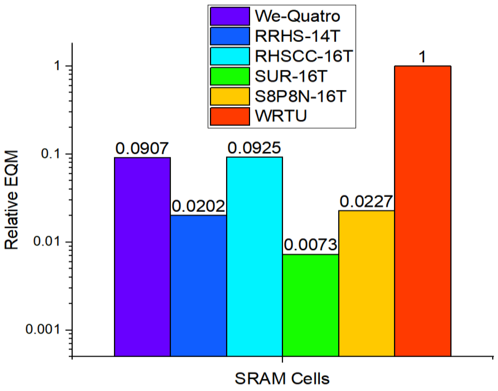
3.8. Electrical Quality Metric

In SRAM design, a balance is required among various electrical characteristics such as static noise margin, access speed, and power consumption, and these characteristics often show a trade-off relationship. For example, increasing the transistor size improves SNM or access speed, but at the same time, the area and power consumption also increases. The performance metrics are summarized in Table 1. To comprehensively evaluate these complex interrelationships, this study proposes an electrical quality metric (EQM) that can quantitatively compare the electrical performance of SRAMs.
The EQM is expressed as a single numerical value that integrates various design indices such as the RSNM, RAT, WAT, WWTV, HPWR, and Qc, and can quantitatively compare the performance of different SRAM structures. As shown in Figure 14, the WRTU-16T recorded the highest EQM value among the five compared SRAMs, which was up to 136 times higher than that of the SUR-16T and at least 11 times higher than that of the RHSCC-16T [14].

4. Conclusions

Radiation-hardened SRAM is proposed, which is optimized for high reliability in radiation environments such as space. The WRTU-16T has a read-decoupled architecture and a charge-sharing suppression mechanism to enhance resilience against soft errors, including SEU. By isolating the storage nodes and applying a feedback loop structure, the WRTU-16T enables rapid recovery and maintains data integrity even under severe radiation exposure. Compared to existing radiation-hardened SRAMs, the proposed WRTU-16T demonstrates several advantages. First, it achieves great performance, such as a WAT of 13.39 ps and WWTV of 366.13 mV, and a low HPWR of 57.93 nW, thereby simultaneously realizing high-speed operations and low power consumption. Second, it exhibits better radiation tolerance and overall electrical robustness, with a Qc exceeding 100 fC and up to a 164 times improvement in the EQM compared to benchmarks. Third, the layout-level physical separation of sensitive nodes (3.11 μm) combined with a dual-feedback structure maximizes recovery capabilities against SEU. While the RSNM of 119 mV is lower than that of several recent cells, this limitation can be mitigated by system-level techniques such as ECC, or it can be improved by changing the transistor sizing ratio, especially the access CR or pull-down ratio.

Author Contributions

Conceptualization, S.-H.L. and S.-H.J.; methodology, S.-H.L.; validation, S.-H.L.; data curation, S.-H.L.; writing—original draft preparation, S.-H.L.; writing—review and editing, S.-H.J.; visualization, S.-H.L.; supervision, S.-H.J.; project administration, S.-H.J. All authors have read and agreed to the published version of the manuscript.

Funding

This research received no external funding.

Institutional Review Board Statement

Not applicable.

Informed Consent Statement

Not applicable.

Data Availability Statement

The original contributions presented in this study are included in the article. Further inquiries can be directed to the corresponding author.

Acknowledgments

The EDA Tool was supported by the IC Design Education Center, Korea.

Conflicts of Interest

The authors declare no conflicts of interest.

References

  1. Kim, C.; Lee, D.; Na, J. A Comparison of Reliability and Resource Utilization of Radiation Fault Tolerance Mechanisms in Spaceborne Electronic Systems. Aerospace 2025, 12, 152. [Google Scholar] [CrossRef]
  2. Trang Dang, L.D.; Kim, J.S.; Chang, I.J. We-Quatro: Radiation-Hardened SRAM Cell With Parametric Process Variation Tolerance. IEEE Trans. Nucl. Sci. 2017, 64, 2489–2496. [Google Scholar] [CrossRef]
  3. Bai, N.; Wang, F.; Xu, Y.; Wang, S.; Wen, X. Reconfigurable Radiation-Hardened SRAM Cell Design for Different Radiation Environments. IEEE Trans. Comput.-Aided Des. Integr. Circuits Syst. 2025, 1, 1. [Google Scholar] [CrossRef]
  4. Bharti, P.K.; Mekie, J. RHSCC-16T: Radiation Hardened Sextuple Cross Coupled Robust SRAM Design for Radiation Prone Environments. In Proceedings of the 2022 IEEE 40th International Conference on Computer Design (ICCD), Olympic Valley, CA, USA, 23–26 October 2022; pp. 17–24. [Google Scholar]
  5. Mukku, P.K.; Lorenzo, R. A Soft Error Upset Recovery SRAM Cell for Aerospace and Military Applications. In Proceedings of the TENCON 2023-2023 IEEE Region 10 Conference (TENCON), Chiang Mai, Thailand, 31 October 2023; pp. 744–749. [Google Scholar]
  6. Bai, N.; Xiao, X.; Xu, Y.; Wang, Y.; Wang, L.; Zhou, X. Soft-Error-Aware SRAM With Multinode Upset Tolerance for Aerospace Applications. IEEE Trans. Very Large Scale Integr. VLSI Syst. 2024, 32, 128–136. [Google Scholar] [CrossRef]
  7. Yao, R.; Lv, H.; Zhang, Y.; Chen, X.; Zhang, Y.; Liu, X.; Bai, G. A High-Reliability 12T SRAM Radiation-Hardened Cell for Aerospace Applications. Micromachines 2023, 14, 1305. [Google Scholar] [CrossRef] [PubMed]
  8. Jiang, J.; Xu, Y.; Zhu, W.; Xiao, J.; Zou, S. Quadruple Cross-Coupled Latch-Based 10T and 12T SRAM Bit-Cell Designs for Highly Reliable Terrestrial Applications. IEEE Trans. Circuits Syst. Regul. Pap. 2019, 66, 967–977. [Google Scholar] [CrossRef]
  9. Kim, K.; Oh, T.W.; Jung, S.-O. Bitline Charge Sharing Suppressed Bitline and Cell Supply Collapse Assists for Energy-Efficient 6T SRAM. IEEE Access 2021, 9, 57393–57403. [Google Scholar] [CrossRef]
  10. Grossar, E.; Stucchi, M.; Maex, K.; Dehaene, W. Read Stability and Write-Ability Analysis of SRAM Cells for Nanometer Technologies. IEEE J. Solid-State Circuits 2006, 41, 2577–2588. [Google Scholar] [CrossRef]
  11. Alorda, B.; Carmona, C.; Torrens, G.; Bota, S. An Affordable Experimental Technique for SRAM Write Margin Characterization for Nanometer CMOS Technologies. Microelectron. Reliab. 2016, 65, 280–288. [Google Scholar] [CrossRef]
  12. Liu, C.; Liu, H.; Yang, J. A Novel Low-Power and Soft Error Recovery 10T SRAM Cell. Micromachines 2023, 14, 845. [Google Scholar] [CrossRef] [PubMed]
  13. Jahinuzzaman, S.M.; Sharifkhani, M.; Sachdev, M. An Analytical Model for Soft Error Critical Charge of Nanometric SRAMs. IEEE Trans. Very Large Scale Integr. VLSI Syst. 2009, 17, 1187–1195. [Google Scholar] [CrossRef]
  14. Thirugnanam, S.; Soong, L.W.; Prabhu, C.M.; Singh, A.K. Energy-Efficient and Variability-Resilient 11T SRAM Design Using Data-Aware Read–Write Assist (DARWA) Technique for Low-Power Applications. Sensors 2023, 23, 5095. [Google Scholar] [CrossRef] [PubMed]
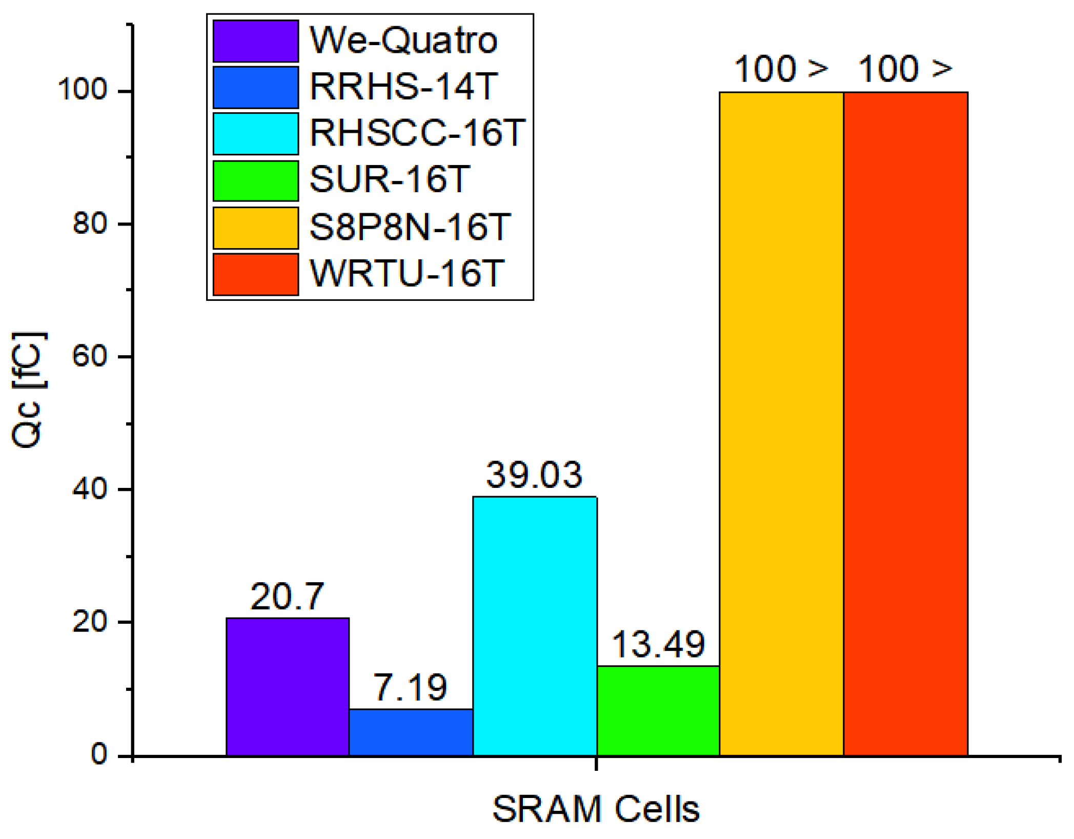
Figure 1. Schematic of the proposed WRTU-16T.
Applsci 15 07295 g001
Figure 2. The cell layout of the proposed WRTU-16T.
Applsci 15 07295 g002
Figure 3. Basic operation results of WRTU-16T.
Applsci 15 07295 g003
Figure 4. Waveform of SEU recovery of WRTU-16T.
Applsci 15 07295 g004
Figure 5. RAT measurement method.
Applsci 15 07295 g005
Figure 6. Comparison of RAT with other SRAMs: (a) at VDD = 1 V, (b) at various VDD levels from 0.9 V to 1.1 V.
Applsci 15 07295 g006
Figure 7. Comparison of RSNM with other SRAMs: (a) at VDD = 1 V, (b) RSNM Measurement.
Applsci 15 07295 g007
Figure 8. WAT and WWTV measurement method.
Applsci 15 07295 g008
Figure 9. Comparison of WAT with other SRAMs: (a) at VDD = 1 V, (b) at various VDD levels from 0.9 V to 1.1 V.
Applsci 15 07295 g009
Figure 10. Comparison of WWTV with other SRAMs: (a) at VDD = 1 V, (b) at various VDD levels from 0.9 V to 1.1 V.
Applsci 15 07295 g010
Figure 11. Comparison of HPWR with other SRAMs: (a) at VDD = 1 V, (b) at various VDD levels from 0.9 V to 1.1 V.
Applsci 15 07295 g011
Figure 12. Comparison of critical charge (Qc) with other SRAMs.
Applsci 15 07295 g012
Figure 13. Recovery waveforms at sensitive nodes following a single-node upset: (a) at Node Q, (b) at Node S0.
Applsci 15 07295 g013
Figure 14. Comparison of relative EQM with other SRAMs.
Applsci 15 07295 g014
Table 1. Performance comparison.
SRAMsQc (fC)RAT (ps)RSNM (mV)WAT (ps)WWTV (mV)HPWR (nW)
We-Quatro [2]20.7034.1628432.15178.5399.29
RRHS-14T [3]7.19186.3930020.87291.3275.52
RHSCC-16T [4]39.0336.6828535.90145.84125.56
SUR-16T [5]13.49101.1222393.7864.4326.51
S8P8N-16T [6]>100149.647835.61143.8487.57
WRTU-16T>10052.9511913.39366.1357.93
Disclaimer/Publisher’s Note: The statements, opinions and data contained in all publications are solely those of the individual author(s) and contributor(s) and not of MDPI and/or the editor(s). MDPI and/or the editor(s) disclaim responsibility for any injury to people or property resulting from any ideas, methods, instructions or products referred to in the content.

