Article

MAS-YOLO: A Lightweight Detection Algorithm for PCB Defect Detection Based on Improved YOLOv12

by
Xupeng Yin
1,2,
Zikai Zhao
2 and
Liguo Weng
1,*
1
Jiangsu Key Laboratory of Big Data Analysis Technology, Nanjing University of Information Science and Technology, Nanjing 210044, China
2
Collaborative Innovation Center on Atmospheric Environment and Equipment Technology, Nanjing University of Information Science and Technology, Nanjing 210044, China
*
Author to whom correspondence should be addressed.
Appl. Sci. 2025, 15(11), 6238; https://doi.org/10.3390/app15116238
Submission received: 19 April 2025 / Revised: 28 May 2025 / Accepted: 30 May 2025 / Published: 1 June 2025
(This article belongs to the Special Issue Big Data Analysis and Management Based on Deep Learning: 2nd Edition)

Abstract

As the performance requirements for printed circuit boards (PCBs) in electronic devices continue to increase, reliable defect detection during PCB manufacturing is vital. However, due to the small size, complex categories, and subtle differences in defect features, traditional detection methods are limited in accuracy and robustness. To overcome these challenges, this paper proposes MAS-YOLO, a lightweight detection algorithm for PCB defect detection based on improved YOLOv12 architecture. In the Backbone, a Median-enhanced Channel and Spatial Attention Block (MECS) expands the receptive field through median enhancement and depthwise convolution to generate attention maps that effectively capture subtle defect features. In the Neck, an Adaptive Hierarchical Feature Integration Network (AHFIN) adaptively fuses multi-scale features through weighted integration, enhancing feature utilization and focus on defect regions. Moreover, the original YOLOv12 loss function is replaced with the Slide Alignment Loss (SAL) to improve bounding box localization and detect complex defect types. Experimental results demonstrate that MAS-YOLO significantly improves mean average precision (mAP) and frames per second (FPS) compared to the original YOLOv12, fulfilling real-time industrial detection requirements.

1. Introduction

With the widespread adoption of electronic devices, printed circuit boards, as the core components of electronic products [1,2], have a direct impact on overall product performance and reliability. Nonetheless, defects like Short circuits, Open circuits, and missing solder joints are common occurrences during the manufacturing process. These defects may result in functional failures or even pose safety risks. Therefore, rapid and accurate PCB defect detection is crucial for improving production efficiency and ensuring product quality. Currently, methods for detecting PCB defects are generally divided into two types: manual inspection and automated detection approaches [3,4,5,6]. Manual inspection depends heavily on the experience and skill level of human operators. However, with increasingly complex circuit designs and growing production scales, manual methods have become inefficient and are susceptible to human subjectivity, making them inadequate for meeting industrial-level demands.
Within automated methods, machine vision-based automated optical inspection (AOI) is commonly utilized [7,8,9]. AOI systems use cameras to scan PCBs and rely on optical principles, frequency domain transformations, and statistical analysis to detect defects [10,11]. Despite their effectiveness, traditional AOI systems often require complex setups involving lighting, mechanical transport, and image acquisition modules, which occupy significant space on the production line and incur high deployment costs. Moreover, these systems typically require professional engineers to pre-program detection logic for different types of PCBs. As a result, detection accuracy is highly dependent on programming quality, making the system difficult to use and poorly generalizable. In scenarios where PCB models change frequently and production batches are small, the programming workload increases significantly, reducing classification efficiency. Additionally, conventional AOI systems often generate a high number of false positives during defect identification.
In recent years, deep learning technologies have achieved remarkable progress in the field of object detection [12,13,14,15,16]. Anitha D et al. [17] employed image processing techniques to pre-classify PCB defects, significantly improving the accuracy of both bare and assembled PCB defect detection. However, the overall workflow remained insufficiently automated and relatively complex. Ling Q et al. [18] proposed a lightweight neural network for PCB defect detection, though the study also pointed out that the model exhibited limited generalization capability when dealing with defects of varying types and sizes. Zhang H et al. [19] introduced a cost-sensitive residual convolutional neural network for visual PCB defect detection, showing potential in enhancing accuracy. Nevertheless, the model required large-scale training data, leading to high computational costs and long training times. Similarly, recent transformer-based detectors and NAS-optimized models have shown great potential in various detection tasks. For instance, the transformer-based detector for object detection has achieved high accuracy in scenarios involving sequential multi-frame images by identifying patterns across frames. However, its applicability to industrial defect detection, especially in managing the intricate and varied defect patterns commonly found in PCBs, has yet to be established. Additionally, although the transformer-based NAS predictor with a self-evolution framework represents a significant step forward in model optimization, its feasibility and effectiveness in real-time industrial environments remain to be fully explored. These limitations indicate the necessity for further research to tailor and enhance these advanced architectures for specialized industrial applications such as PCB defect detection.
The YOLO series of algorithms has emerged as a prominent research focus due to its real-time performance and computational efficiency [20,21,22,23,24,25]. The original YOLO algorithm proposed by Redmon et al. [26] demonstrated impressive speed in object detection; however, its bounding box regression accuracy proved inadequate when detecting PCB defects in complex backgrounds. Adibhatla et al. [27] focused on the challenge of small object detection within PCB inspection, yet the proposed model suffered from limited feature extraction capacity and low classification efficiency, rendering it unsuitable for intricate industrial classification tasks. Yuan et al. [28] enhanced the YOLOv5s algorithm to improve PCB defect classification, but limitations in feature extraction and multi-scale fusion reduced its effectiveness in handling defects across scales. Shi et al. [29] introduced an improved YOLOv7-tiny model to enhance small object detection, achieving performance gains; however, further reduction in model size and computational complexity remains necessary. Chen et al. [30] proposed modifications to the YOLOv8 architecture by introducing a more effective feature fusion mechanism, improving detection accuracy for surface-level PCB defects, but challenges persist regarding computational complexity and frame rate optimization.
To address the aforementioned limitations, this paper proposes a PCB defect detection model based on an enhanced YOLOv12 framework. Specifically, a Median-enhanced Channel and Spatial Attention Block (MECS) is integrated into the Backbone to enhance feature extraction performance and robustness through an improved attention mechanism that expands the receptive field using median enhancement and depthwise convolution. In the Neck, an Adaptive Hierarchical Feature Integration Network (AHFIN) is introduced, which employs adaptive Deformable Convolution and gradient compression to fuse multi-scale features, thereby strengthening the model’s focus on critical defect regions. In addition, the original YOLOv12 loss function is replaced with the Slide Alignment Loss (SAL) to optimize bounding box regression and address sample imbalance. Experimental results confirm that the proposed MAS-YOLO model consistently delivers superior performance across multiple PCB defect datasets, effectively meeting the requirements for real-time industrial detection.

2. Methodology

2.1. Original YOLOv12 Algorithm

YOLOv12 is a convolutional neural network-based object detection algorithm that employs an end-to-end approach for both training and inference [31,32]. In YOLOv12, the network architecture primarily consists of four components: the input layer, the Backbone [33], the Neck network [34], and the detection Head. The Backbone is responsible for feature extraction, utilizing a deep convolutional neural network architecture to extract features from the input images through multiple convolutional layers. The C3k2 and A2C2f modules are incorporated to further refine these features. The Neck is primarily used for multi-scale feature fusion, employing techniques such as the feature pyramid network (FPN) [35,36] and the Path Aggregation Network (PAN) [37] to enhance the detection of small objects. The Head handles the final object classification and bounding box regression. The advantage of YOLOv12 lies in its efficient detection capability and real-time performance, enabling high-precision object detection with relatively low computational cost. Compared with previous YOLO versions, YOLOv12 achieves improvements in both detection speed and accuracy, and its adoption of an Anchor-Free mechanism simplifies the traditional Anchor-Based design, thereby reducing inference latency.

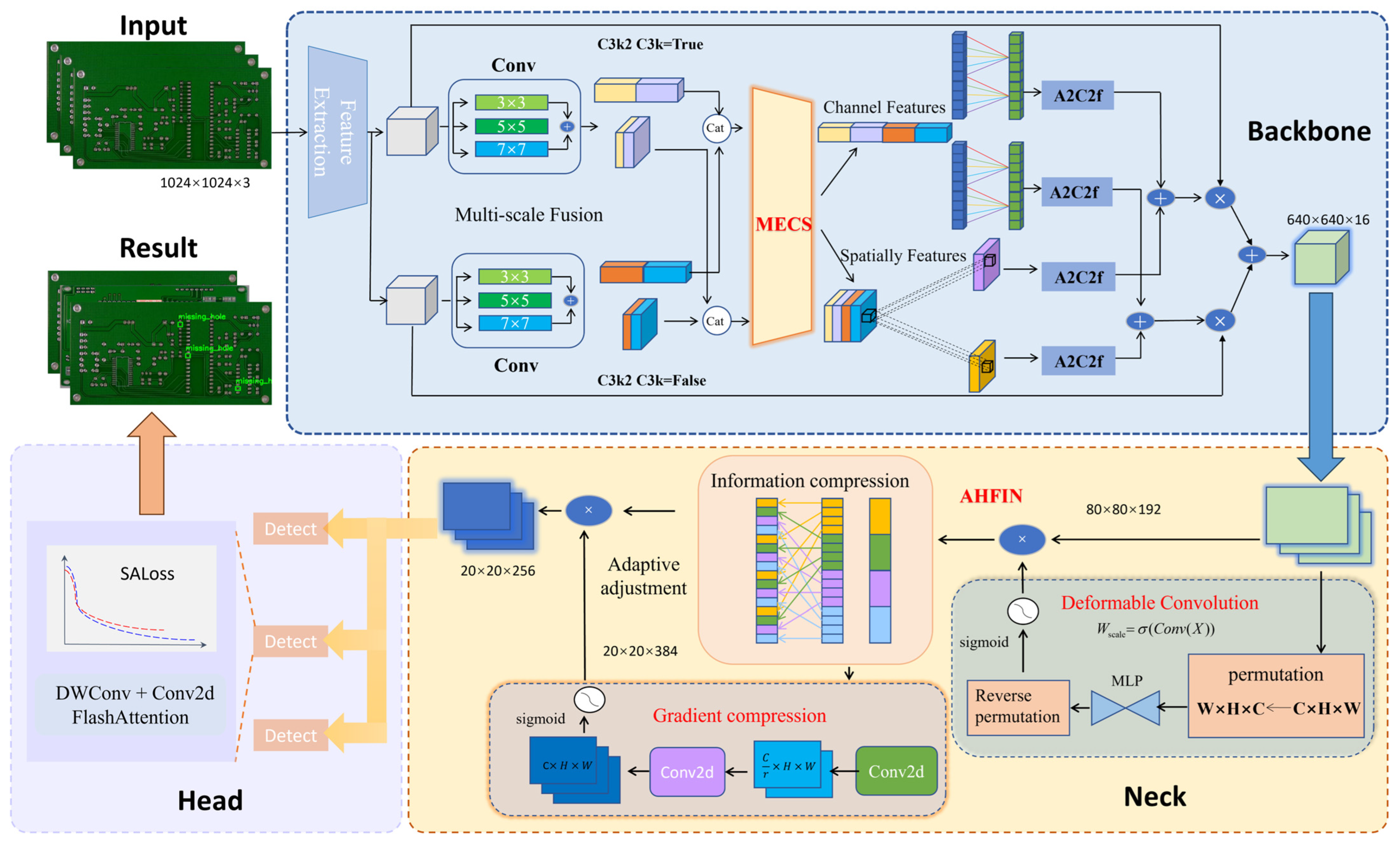
2.2. Improved YOLOv12 Algorithm

Based on YOLOv12, this paper proposes an improved algorithm for PCB defect detection—MAS-YOLO. The model is optimized in three main aspects to enhance both detection accuracy and robustness for PCB defects. The overall framework of the improved YOLOv12 algorithm is shown in Figure 1.
First, a Median-enhanced Channel and Spatial Attention Block is integrated into the Backbone. Unlike conventional attention mechanisms that may struggle with noise suppression in complex industrial settings, the MECS module innovatively combines median enhancement with depthwise convolution. This unique fusion not only broadens the receptive field but also selectively amplifies defect-specific features while robustly mitigating noise interference, a critical advancement over prior arts where noise can significantly degrade detection accuracy. Second, the Adaptive Hierarchical Feature Integration Network is introduced in the Neck. While multi-scale feature fusion is a common strategy, AHFIN distinguishes itself through its adaptive Deformable Convolution and gradient compression. Unlike static fusion methods, AHFIN dynamically recalibrates feature importance across scales, effectively capturing the hierarchical nature of PCB defects. This dynamic adjustment is particularly advantageous in PCB inspection, where defects of varying morphologies necessitate a flexible feature integration approach. Third, the original YOLOv12 loss function (CIoU) is substituted with the Slide Alignment Loss. Traditional loss functions often fail to adequately address the geometric complexities of PCB defects, such as irregular shapes and inconsistent orientations. SAL introduces a novel adaptive weighting scheme that holistically considers center deviation, size ratio, and angle differences. This comprehensive approach not only refines bounding box regression but also inherently compensates for sample imbalance, a limitation that has persisted in previous frameworks.
When contrasted with similar works like SSHP-YOLO [24], YOLO-MBBi [25], and YOLO-DHGC [30], MAS-YOLO’s originality lies in its cohesive and synergistic architecture. While these prior models incorporate elements such as multi-scale fusion and adaptive losses, MAS-YOLO uniquely integrates median-enhanced attention, adaptive hierarchical fusion, and geometry-aware loss optimization within a unified framework. This integration is not merely incremental but represents a substantial advancement in addressing the specific challenges of PCB defect detection. For instance, SSHP-YOLO focuses on enhancing Backbone features through multi-branch blocks but lacks the sophisticated attention and loss mechanisms present in MAS-YOLO. YOLO-MBBi, while effective in high-precision detection, does not achieve the same level of computational efficiency and adaptability across diverse defect morphologies as MAS-YOLO. Similarly, YOLO-DHGC employs dense connections for feature enhancement but does not incorporate the geometric and noise-aware refinements that MAS-YOLO introduces.
Through these improvements, the MAS-YOLO model demonstrates enhanced detection accuracy and real-time performance in PCB defect detection tasks, thereby meeting the dual requirements of detection speed and accuracy in industrial applications. The following sections provide a detailed explanation of the improved modules and loss function.

2.2.1. Median-Enhanced Channel and Spatial Attention Block (MECS)

In PCB defect detection tasks, the effective extraction of feature maps is crucial. Defects on PCBs typically manifest as small, localized features and are often affected by complex background interference. The Median-enhanced Channel and Spatial Attention Block module incorporates a median enhancement operation to fuse channel and spatial attention mechanisms. It is designed to significantly improve the model’s feature extraction capability for PCB defects, particularly enhancing robustness in detecting small targets under complex background conditions. The structure of the MECS module is illustrated in Figure 2.
Firstly, the input feature map undergoes three different types of pooling operations. The aim of these pooling operations is to capture the global information of the feature map at different levels and to enhance noise suppression by incorporating the specially introduced median pooling. Since PCB defects are typically small and difficult to extract directly from the overall background, the use of median pooling helps to suppress noise in complex backgrounds while preserving key information. The expressions for these pooling results are as follows:
P a v g   = A v g P o o l ( X ) ,
P m a x   = M a x P o o l ( X ) ,
P m e d   = M e d i a n P o o l ( X ) .
Next, the pooled feature maps are further processed by a Multi-Layer Perceptron (MLP). To enhance the efficiency and effectiveness of feature learning, the MLP first applies a 3 × 3 convolutional layer for dimensionality reduction, followed by a 1 × 1 convolutional layer to restore the channel dimension. This design not only reduces redundant information but also improves the discriminative capability of the features. Finally, the outputs of the MLP are aggregated and passed through a Sigmoid activation function to generate the channel attention weights:
A c h a n n e l   = σ ( M L P ( P a v g   ) + M L P ( P m a x   ) + M L P ( P m e d   ) ) .
where the Sigmoid activation function maps the output values to the range of [0, 1], thereby generating the channel attention map. This attention map is then multiplied element-wise with the original input feature map to perform weighted processing. This operation enhances critical information while suppressing irrelevant background noise. The formulation is expressed as follows:
X w e i g h t e d   = X A c h a n n e l   .
In PCB defect detection, this process enhances the model’s sensitivity to defect features, particularly in identifying subtle circuit anomalies. By emphasizing important channels and suppressing irrelevant background noise from circuit traces, it improves detection precision. The spatial attention mechanism further strengthens the spatial feature extraction capability through multi-scale convolution operations. Given that PCB defects may appear at various locations and exhibit significant variations in scale, the use of multi-scale convolutions facilitates the capture of defect information across different resolutions. In this component, the input feature map is first processed by a 7 × 7 depthwise convolutional layer to extract fundamental spatial features, followed by several depthwise convolutional layers with varying kernel sizes to obtain more refined spatial information. After fusing these multi-scale features, a spatial attention map is generated, whose expression is given as follows:
X f i n a l   = X w e i g h t e d A s p a c e   .
The spatial attention map is multiplied element-wise with the weighted feature map to highlight important defect regions, further enhancing the model’s adaptability to complex backgrounds and multi-scale defects.

2.2.2. Adaptive Hierarchical Feature Integration Network (AHFIN)

The core design of the Adaptive Hierarchical Feature Integration Network focuses on adaptively weighting and integrating multi-scale features to precisely target critical regions of PCB defects, particularly those that are small in size and exhibit diverse morphologies. Given that PCB defects often manifest as localized details against complex backgrounds, traditional methods struggle to simultaneously preserve fine-grained information and global semantic context. AHFIN effectively addresses this challenge through its adaptive mechanisms.
The network first outputs feature maps at different levels through the Backbone network, ranging from shallow to deep layers [38]. Shallow features primarily capture detailed information, while deep features provide global semantic information. For each feature map, a convolutional layer and a Sigmoid activation function are used to generate a weight map that reflects the importance of features at each scale. Specifically, for each feature map, the weight is obtained through the Sigmoid function as follows:
W scale   = σ ( C o n v ( X ) ) .
where σ denotes the Sigmoid activation function, while C o n v X refers to the convolution applied to the input feature map. This weighting diagram allows the network to adaptively adjust the importance of each feature based on the different scales of the feature map.
To ensure spatial alignment across features of different scales, AHFIN incorporates lightweight Deformable Convolutions to spatially calibrate low-resolution features. After alignment, the multi-scale features are adaptively fused according to their respective weights, resulting in an integrated feature map, which can be expressed as follows:
X fused = i = 1 N W scale X i .
where W scale represents the weight of the i -th scale, X i denotes the feature map of the i -th scale, and the symbol ⊙ indicates element-wise multiplication. The integrated feature map retains both shallow-level details and deep-level semantics, which helps enhance the detection capability for complex shapes and minor defects.
Finally, the fused features are further processed through a gradient compression module to reduce dimensionality, followed by the introduction of residual connections to ensure efficient information flow throughout the network. This process enhances gradient propagation and improves the model’s robustness, thereby strengthening its ability to detect defects in complex scenarios. By integrating Deformable Convolution for spatial alignment and gradient compression for dimensionality reduction, AHFIN significantly improves sensitivity and processing efficiency for small and complex-shaped defects in PCB defect detection tasks. In particular, it substantially enhances the model’s capability to identify subtle defects within cluttered backgrounds.

2.2.3. Slide Alignment Loss (SAL)

In PCB defect detection, targets are typically small in size and exhibit irregular shapes. The traditional CIoU loss function shows limitations in addressing issues such as mismatched aspect ratios and angle deviations of bounding boxes. To overcome these challenges, this paper proposes Slide Alignment Loss, a loss function that not only considers center deviation, size ratio, and angle differences but also incorporates an adaptive weighting mechanism for sample difficulty, thereby enabling more precise bounding box regression.
The SAL function is composed of multiple parts. First, the center distance loss is used to measure the normalized error between the predicted box center and the true box center, with the formula given by the following:
L center = 1 C C pred C true .
where C p r e d and C t r u e represent the predicted and actual box centers, respectively, and C is used for normalization to ensure that errors are comparable across different sizes.
Secondly, the size ratio loss is used to compute the relative differences in width and height between the predicted bounding box and the ground truth. By evaluating the ratio of dimensions between the predicted and ground truth boxes, the SAL function can better adjust the shape of the target bounding box to more closely match the ground truth.
To address the discrepancy in rotation angles, SAL introduces an angular deviation loss. This loss is calculated by measuring the cosine similarity between the predicted and true bounding boxes to quantify the inconsistency in their angles:
L angle = 1 cos ( θ pred θ true ) .
where θ pred and θ true represent the rotation angles of the predicted and true bounding boxes, respectively. The rotation angle θ is defined as the angle between the bounding box’s orientation and a reference axis, typically ranging from −π/2 to π/2. For detected samples, θ pred is obtained directly from the model’s output, while θ true is derived from the ground truth annotation. The cosine similarity is computed using the dot product of the two angle vectors divided by the product of their magnitudes. This loss is particularly effective for handling irregular shapes on PCBs, effectively addressing the alignment issue of rotation angles.
Moreover, the angular deviation loss innovatively incorporates a dynamic angle adjustment mechanism. This mechanism adaptively adjusts the weight of the angle loss based on the difference between θ pred and θ true . When the angle difference is large, the weight is increased to prioritize aligning the rotation angles. Conversely, when the angle difference is small, the weight is reduced to focus more on other aspects of the bounding box regression. This dynamic adjustment enhances the model’s ability to converge more effectively on accurate angle predictions.
The gradient of the angular deviation loss with respect to the model’s predictions is computed as follows: Let θ pred be the predicted angle and θ true be the true angle. The gradient L angle θ pred is given by the following:
L angle θ pred = sin ( θ pred θ true ) .
This gradient is then backpropagated through the network to update the model’s parameters, allowing it to learn the correct alignment of bounding box angles. The dynamic angle adjustment mechanism ensures that the model not only learns the correct angles but also does so efficiently, leading to improved performance in detecting defects with varying orientations.
Furthermore, most importantly, to enhance the model’s ability to detect hard examples, SAL introduces a weight matrix factor R S A L for pixel-wise weighting:
R SAL = exp ( ( x x g t ) 2 + ( y y g t ) 2 W g 2 + H g 2 * ) .
To prevent R S A L from generating gradients that impede convergence, W g   and H g   are decoupled from the computation graph. Here, W g   and H g   denote the width and height of the minimum bounding box, respectively. This matrix can be customized based on pixel importance, such as object type, pixel position, or pixel difficulty. R S A L is used in the weighted calculation of intersection and area to get L sample :
L sample = r R SAL L IoU .
The expression for   r is given by r = β δ α β δ . Here, β constructs a non-monotonic focusing factor that defines the degree of clustering and describes the quality of the Anchor boxes. A higher degree of clustering indicates better Anchor box quality.
Finally, SAL computes the total loss as the weighted sum of the losses described above:
L SAL = λ 1 L center + λ 2 L angle + λ 3 L sample .
where λ1, λ2, and λ3 are hyperparameters used to balance the contributions of each loss component.
For PCB inspection scenarios with small-sized targets that have significant morphological variations and inconsistent rotation angles, the SAL function enables more precise bounding box regression by comprehensively considering errors in center, size, and angle. At the same time, by utilizing an adaptive weighting mechanism, SAL can focus on difficult samples with low IoU, further enhancing overall detection performance.

3. Experiment and Analysis

3.1. Datasets

In this study, two publicly available PCB defect detection datasets were selected: the Kaggle PCB Defects dataset and the Peking University Intelligent Robotics Open Laboratory public PCB defect dataset. These images were captured in industrial production environments and are annotated with six common defect types (as shown in Figure 3), including Missing hole, Mouse bite, Open circuit, Short, Spur, and Spurious copper, closely aligning with real-world PCB defect detection scenarios.

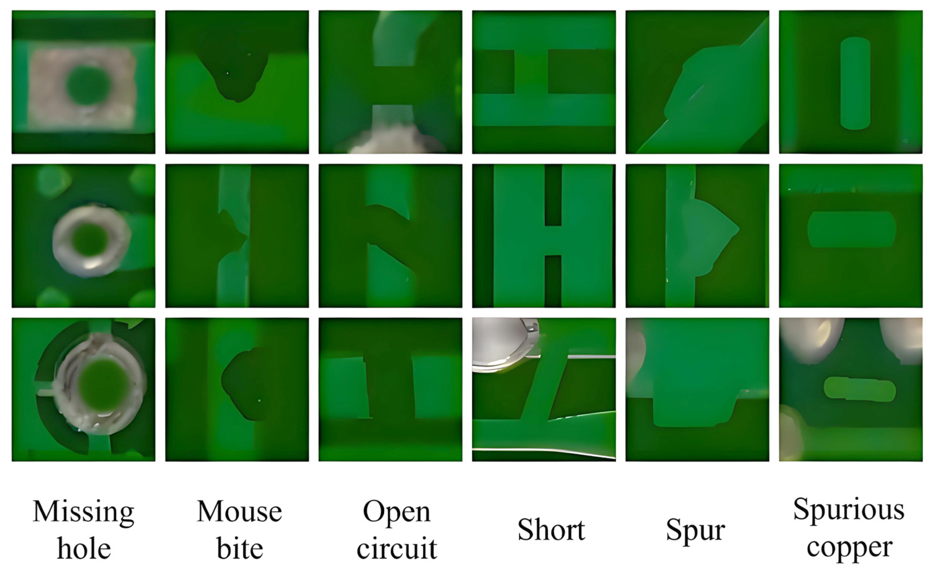
3.1.1. Peking University PCB Defects Dataset

The Peking University PCB dataset contains 1386 images, each exhibiting high clarity and detail. To better adapt the model to real-world industrial environments, the original dataset underwent several preprocessing operations. These operations include brightness correction, which involved randomly adjusting the image brightness to 0.5 to 1.5 times the original brightness to simulate varying lighting conditions in industrial settings; random noise addition, which employed Gaussian noise with a mean of 0 and a standard deviation between 0.05 and 0.15, as well as salt-and-pepper noise with a density of 0.05 to 0.2; rotational transformations conducted within the range of −30 to 30 degrees in 5-degree increments; and horizontal and vertical mirroring, which involved simple mirror flipping of the images. As a result of these processes, a total of 3000 images with a resolution of 1024 × 1024 were generated. To ensure both effective training and robust generalization, a scientifically sound data splitting strategy was adopted: 2000 images were randomly selected as training samples, 500 images were used as a validation set for tuning hyperparameters, and the remaining 500 images were reserved as a test set for the final evaluation of model performance.

3.1.2. Kaggle PCBA Defects Dataset

The Kaggle PCBA Defects dataset contains approximately 2000 images. Notably, these images were captured by a high-definition industrial camera equipped with a 16-megapixel CMOS sensor from various angles (top, side, and oblique). Moreover, to accommodate different PCB sizes and prevent edge distortion, the camera is fitted with a distortion-free zoom industrial lens, featuring an adjustable focal length between 6 and 12 mm and a maximum aperture of f/1.6. In order to avoid mirror reflections and potential shadows on the board, and to minimize the impact of uneven lighting on subsequent processing steps, two frosted annular LED light sources equipped with special diffusion and extinction plates were introduced. This setup effectively mitigates the adverse effects of lighting, thereby closely mirroring actual industrial processes. The original images are 4608 × 3456 pixels in resolution; however, due to GPU limitations, the initial dataset was partitioned into 3000 samples, each with a resolution of 1024 × 1024 pixels. These samples were subsequently split into training, validation, and test sets following a 4:1:1 ratio. It is important to note that the training, validation, and test sets are maintained as distinct and non-overlapping subsets to prevent data leakage and ensure the integrity of the evaluation process.

3.2. Introduction to Experimental Environment and Indicators

In this study, the experimental training environment was setup on a high-performance server equipped with four GeForce RTX 3050Ti GPUs, running Ubuntu, and the development framework was chosen as PyTorch-GPU (python = 3.10). During the model training phase, meticulous adjustments were made to the hyperparameters to ensure effective learning and convergence to an optimal performance state.
Specifically, the learning rate was set to 0.01; this relatively high initial learning rate facilitates rapid convergence during the early stages of training and is adjusted in a timely manner based on validation set performance to prevent premature convergence to local optima. Based on preliminary experiments, this study decided to conduct 300 training iterations during the optimal training process. This choice of epoch number was based on a careful balance between ensuring sufficient training for the model to learn the complex patterns in the data and avoiding unnecessary consumption of computational resources. Moreover, to ensure that the model did not overfit the training data, early stopping criteria were considered. Specifically, if the validation loss trend did not change for a certain number of epochs (e.g., 10 epochs), the training process would terminate early. A batch size of 16 was selected, striking a good balance between training stability and GPU memory utilization. For the optimizer, Stochastic Gradient Descent (SGD) was adopted due to its simplicity and effectiveness, and its widespread application in deep learning provides a stable optimization pathway for model training.
To better align with the actual hardware conditions of industrial inspection and to more accurately assess the model’s performance, this study transplanted the trained model to the Jetson Xavier NX embedded platform for application testing. In terms of model performance evaluation, the key metrics focused on in this study include precision, recall, mean average precision (mAP), model parameter count (parameters), computational complexity (GFLOPs), and detection frame rate (FPS).
Precision is used to measure the risk of the classifier incorrectly classifying negative examples as positive. The calculation formula for precision is as follows:
P = TP TP + FP .
Recall quantifies the percentage of True Positive instances correctly identified by the model, serving as an indicator of its detection effectiveness. The calculation formula for recall is as follows:
R = TP TP + FN ,
where True Positive (TP) refers to correctly predicted positive cases. False Positive (FP) indicates incorrect negative predictions for actual positive cases, while False Negative (FN) refers to missed positive cases predicted as negative.
Mean average precision (mAP) offers an integrated evaluation of the model’s trade-off between precision and recall across various defect types, making it a crucial metric for assessing overall detection performance:
m A P = 1 N i = 1 N A P i
Model parameters (parameters) reflect the complexity and storage requirements of the model. Computational complexity (GFLOPs) measures the amount of computation required during inference, which is closely related to the model’s operational efficiency. Detection frame rate (FPS) directly indicates the model’s real-time performance in practical applications, which is crucial for meeting the real-time detection demands in industrial production.
A comprehensive evaluation of these metrics allows for a thorough assessment of the model’s performance in PCB defect detection, providing a solid foundation for further optimization and practical implementation.

3.3. Experimental Process

3.3.1. Comparison of Detection Performance Across Different Basic Models

In a carefully controlled and unified experimental environment, a comprehensive and systematic comparative analysis was performed to evaluate the performance of several of the most recent and widely recognized object detection algorithms on two distinct datasets: the Kaggle PCBA Defects dataset and the Peking University PCB Defects dataset. The selected algorithms include SSD, CNN, Mask R-CNN, RetinaNet, EfficientDet, YOLOv8, and YOLOv12.
SSD (Single Shot Multibox Detector) is a real-time object detection algorithm that predicts object classes and locations directly from fixed-size input images. It uses a series of convolutional layers to produce predictions, making it efficient for real-time applications. CNN (convolutional neural network) forms the Backbone of many object detection models, using convolutional layers to extract features from images. It is characterized by its depth and the use of multiple layers to learn hierarchical features. Mask R-CNN extends Faster R-CNN to predict instance masks in addition to bounding boxes and classes, making it suitable for instance segmentation tasks. It introduces a branch for predicting object masks, thus enabling precise localization. RetinaNet addresses the class imbalance problem in object detection with a focal loss function, improving performance on small objects. It uses a ResNet Backbone and a feature pyramid network to handle objects at different scales. EfficientDet balances efficiency and accuracy through a balanced architecture and compound scaling method. It scales the network in a balanced way to achieve optimal performance across different resource constraints.
For a fair comparison, all models were trained under the same experimental conditions. Specifically, the learning rate was set to 0.01, and training was conducted for 300 epochs with a batch size of 16. The optimizer used was Stochastic Gradient Descent (SGD) due to its simplicity and effectiveness.
Table 1 details the performance metrics of each algorithm on the Kaggle PCBA Defects dataset, while Table 2 presents the results for the Peking University PCB Defects dataset. This analysis offers valuable insights into the relative efficiency and applicability of these methods, helping to identify the most suitable algorithms for PCB defect detection tasks.
The experimental results demonstrate that YOLOv12 exhibits significant advantages across multiple key metrics on both datasets. For the Kaggle PCBA Defects dataset, YOLOv12 achieved a mean average precision of 85.3%, ranking highest among all compared models. Although its model size of 12.8 MB is slightly larger than that of SSD and RetinaNet, this is acceptable given the substantial improvement in accuracy. In terms of computational complexity, YOLOv12 reaches 22.4 GFLOPs—higher than EfficientDet’s 19.1 and RetinaNet’s 16.8—but its detection frame rate hits 47.2 frames per second, the fastest among all algorithms. For the Peking University PCB Defects dataset, YOLOv12 also attained the highest mAP at 84.2%. Its FPS reached 48.0, second only to RetinaNet, indicating excellent detection speed. While YOLOv12’s model size is 12.4 MB, slightly larger than SSD and RetinaNet, the balance it strikes between accuracy and speed makes it more favorable for real-time applications. Other models, such as Mask R-CNN, showed comparable accuracy but suffered from significantly lower FPS (only 11.2), limiting their suitability for time-sensitive industrial scenarios.
Through this comprehensive analysis, it is evident that YOLOv12—thanks to its single-stage architecture and lightweight, efficient design—performs exceptionally well in terms of detection accuracy, processing speed, and resource utilization. As a result, YOLOv12 was selected as the base model for further improvement.

3.3.2. Performance Evaluation and Comparative Experiments of MECS Module

The MECS module was integrated between the Neck and the prediction network of the model. Its performance was compared on both datasets against the baseline YOLOv12 model and a variant incorporating the classic spatial-channel attention module CBAM [39,40]. The experimental results are summarized in Table 3 and Table 4.
For the Kaggle PCB Defects dataset, the integration of the MECS module significantly enhanced the model’s mean average precision, increasing from 85.3% to 92.0%, a notable gain of 6.7%. Additionally, compared to the YOLOv12 + CBAM model, the mAP also showed a 4.8 percentage point increase. It is noteworthy that despite the significant increase in mAP, the model’s frame rate only decreased slightly from 47.2 frames per second to 47.1 frames per second, showing almost no impact.
In the Peking University PCB Defects dataset test, the YOLOv12 + MECS model’s average precision increased from 84.2% to 91.7%, a rise of 7.5 percentage points. Compared to YOLOv12 + CBAM, the mAP improved by 3.6 percentage points. Although the precision showed a significant improvement, the FPS only dropped from 48.0 to 47.4, with minimal impact. YOLOv12 + MECS maintained a high frame rate while improving precision, making it suitable for real-time applications.
This finding confirms that the MECS module significantly enhances the model’s detection accuracy while maintaining stable frame rates, demonstrating its excellent performance improvement potential in object detection tasks. This performance enhancement is attributed to the innovative design of the MECS pooling layer and convolutional kernels. Unlike the classic channel and spatial attention mechanisms CBAM, the MECS module not only utilizes global average pooling and global max pooling in feature extraction but also incorporates median pooling and multi-scale convolutional kernel designs. These designs help the model handle PCB detection tasks with significant noise, such as reflections, dust occlusions, and physical noise in the input feature maps, by effectively removing noise while preserving important feature information.

3.3.3. Performance Evaluation and Comparative Experiments of AHFIN

In the YOLOv12 model architecture, the AHFIN feature fusion network is embedded into the Neck part of the network, where features from different scales are weighted and fused. A performance comparison is made among the base YOLOv12 model, the model using the classical FPN feature fusion method, and the model incorporating the AHFIN feature fusion network. The experimental results on the two datasets are shown in Table 5 and Table 6, respectively.
The experimental results for the Kaggle PCB Defects dataset indicate that incorporating the AHFIN module enhanced the model’s mean average precision from 85.3% to 89.4%, reflecting a 4.1% increase. Additionally, compared to the YOLOv12 + FPN model, the mAP achieved an improvement of 2.2 percentage points. Moreover, the detection speed also saw a corresponding increase.
For the Peking University PCB Defects dataset, compared to the base YOLOv12 model, after integrating the AHFIN module, the model’s mAP increased from 84.2% to 89.0%, an increase of 4.8 percentage points, and the FPS improved by 1.2 points, showing a notable improvement in both detection accuracy and speed. Compared to the YOLOv12 + FPN model, the mAP also improved by 0.9 percentage points.
Compared to the FPN structure, AHFIN’s lightweight Deformable Convolution performs real-time spatial correction on low-resolution features in PCB defect images and then applies adaptive weighted fusion to features from different scales. This efficient and accurate feature space processing method leads to a higher mAP value. In addition, its unique gradient compression module significantly enhances the detection speed. When handling multi-class and multi-size targets in PCB defect detection, it demonstrates superior performance.

3.3.4. The Comparison of the Impact of Loss Functions on the Training Process

To assess the influence of the Slide Alignment Loss on training performance, the YOLOv12 model was trained using four loss functions: CIoU, DIoU, GIoU, and SAL. The two datasets were merged for the experiments. Figure 4 visualizes the loss curves during the training process. Table 7 presents the loss values obtained from model training with different loss functions over large epochs (from 250 epochs to 400 epochs).
Observing the loss curves in Figure 4 and the loss data in Table 7, it is evident that all loss functions tend to stabilize after approximately 300 epochs. This indicates that the model has effectively learned the underlying data patterns and undergone gradual optimization during training. Among the loss functions, the Slide Alignment Loss (SAL) demonstrates the fastest convergence rate and achieves the lowest loss value, underscoring its superiority in model performance.
The data analysis in Table 7 further reveals that the model’s performance stabilizes between 300 and 400 epochs, with no significant improvements observed from additional training(As shown in the bold data in Table 7). Training beyond this point risks overfitting and incurs unnecessary computational resource consumption. To balance convergence and generalization capabilities, all subsequent model validation experiments were conducted at the 300-epoch mark.
The data in Table 8 further demonstrate that the model trained with SAL outperformed other loss functions in key performance indicators such as mAP, precision, and recall. This is because, unlike other loss functions, the SAL function introduces an adaptive weight factor based on the consideration of center deviation, size ratio, and angle differences. It specifically focuses on difficult samples with varying morphology, size, and angle characteristics of defects by dynamically adjusting its attention based on the difficulty of the samples. This enhances the overall convergence effect of the training process, better balancing precision and recall, and effectively improving the model’s detection accuracy and generalization ability.
Based on the results from the figures and tables, it can be concluded that introducing the SAL function significantly improves the performance of the YOLOv12 model in PCB defect detection tasks, particularly for detecting small-sized and complex, easily confused PCB defects, where its effectiveness is especially remarkable.

3.3.5. Comprehensive Ablation Experiment

To validate the overall performance of the improved algorithm in PCB defect detection, based on the original YOLOv12 model, the MECS module, AHFIN, and Slide Alignment Loss were added separately. The two datasets were merged to conduct a comprehensive ablation experiment analysis of the contributions of each module. The experimental results are shown in Table 9.
When the MECS or AHFIN modules were added individually, the model showed improvements in detection accuracy, precision, and recall. When both modules were integrated together, the performance further improved, indicating that the two modules work synergistically in feature extraction and fusion. Additionally, the final model, MAS-YOLO, which incorporates the MECS module, AHFIN module, and SAL function, showed improvements of 7.8%, 8.0%, and 9.7% in detection accuracy, precision, and recall, respectively, compared to the original model. Furthermore, the detection speed FPS also increased by 2.7 percentage points, demonstrating the best performance. This improvement is attributed to the three pooling layers in the MECS module, which preprocess and suppress image noise in the Backbone section, filtering out important features for attention. Moreover, the use of convolutional kernels of different scales helps capture information in different scales and orientations in the feature map, greatly enhancing the spatial processing efficiency of the subsequent Deformable Convolution in the Neck layer. After noise removal, the workload of the gradient compression module was also reduced, optimizing both detection accuracy and speed. Additionally, the introduction of the SAL function further fine-tunes the model’s ability to classify features of varying scales and shapes, leading to further improvements in detection performance.
To assess the detection performance of the improved model in practical scenarios, the receptive field of PCB defect images was visualized, as depicted in Figure 5. Figure 5a illustrates the receptive field of the original YOLOv12 model, while Figure 5b shows that of the enhanced MAS-YOLO model. It is evident that the improved model, with optimized multi-scale convolutional kernels and reduced noise interference, significantly broadens the effective receptive field for feature extraction. A larger receptive field enables the model to capture more visual details, further validating the enhanced feature extraction capability of the proposed MAS-YOLO.
Figure 6 presents a comparative analysis of the detection performance of the original YOLOv12 and the enhanced MAS-YOLO models across six common PCB defect categories: Missing hole, Mouse bite, Open circuit, Short, Spur, and Spurious copper (subfigures (a) to (f), respectively). Each subfigure juxtaposes the detection outcomes of the two models, with the left side illustrating the original YOLOv12 results and the right side showcasing the MAS-YOLO results.
A detailed examination reveals that the original YOLOv12 model suffers from missed detections and imprecise boundary localization, particularly when confronted with small target defects or intricate backgrounds. For instance, in Figure 6a, the YOLOv12 model fails to accurately identify all instances of Missing hole defects, exhibiting missed detections. Furthermore, the boundary boxes it delineates for certain holes are not precise, failing to accurately outline the complete contours of the Missing hole defects. Similarly, in Figure 6c, the model’s performance on Open circuit defects is subpar, as it struggles to accurately detect subtle Open circuit areas, leading to incomplete detection results.
Conversely, the MAS-YOLO model demonstrates significant advantages following the improvements. It is capable of accurately identifying small defect targets within complex backgrounds and has enhanced the precision of defect boundary localization. Take the Spur defect in Figure 6e as an example, the MAS-YOLO model accurately captures the minute characteristics of the Spur and delineates it with boundary boxes that closely match its actual shape, thereby reducing instances of misjudgment and missed detection. Additionally, in the case of the Spurious copper defect in Figure 6f, the improved model not only accurately identifies the locations of excess copper but also distinguishes them more effectively from normal circuit patterns, thereby significantly enhancing detection accuracy.
Across various defect detection tasks, the MAS-YOLO model delivers outstanding performance. Its confusion matrix for classification detection is depicted in Figure 7. An analysis of the confusion matrix reveals that while there are still extremely few misclassifications between the Missing hole and Open circuit categories, the number of such misclassifications has been substantially reduced compared to the original model. This indicates that the MAS-YOLO model not only improves detection accuracy but also enhances its ability to accurately classify different defect types. Furthermore, refined label preprocessing in the future can further decrease these minor misclassifications.
Using the same merged dataset, the improved MAS-YOLO algorithm was compared with other state-of-the-art detection algorithms for overall performance. The experimental results are shown in Figure 8 and Table 10. Although Zhang’s CS-ResNet model [17] achieves a classification accuracy of 93.7%, slightly higher than this study, its model parameter size and complexity limit its detection frame rate to only 15.1 frames per second, making it unsuitable for real-time detection in production line applications. While Shen’s Faster-RCNN [12] has an advantage in detection frame rate, its mAP value is only 75.8, far below the detection accuracy of this study. Therefore, the MAS-YOLO proposed in this study performs better in both average detection accuracy and real-time detection, making it particularly suitable for real-time defect detection on PCB production lines. It significantly improves detection efficiency and addresses the challenges of identifying complex defect targets.

4. Discussion and Conclusions

To address the challenges of small target features that are difficult to recognize and strong background interference caused by complex wiring in PCB defect detection tasks, this paper proposes a lightweight detection algorithm based on an improved YOLOv12. Through the integration of the Median-enhanced Channel and Spatial Attention Block, which merges channel and spatial attention mechanisms, the feature extraction capability is significantly enhanced, leading to an increase in detection accuracy by 6.7 and 7.5 percentage points on two experimental datasets, respectively, compared to the original YOLOv12. At the same time, an Adaptive Hierarchical Feature Integration Network was designed to achieve adaptive weighted fusion of multi-scale features, effectively improving the model’s ability to detect small defects and adapt to complex scenes. The detection accuracy is further improved by 4.1 and 4.8 percentage points on the two datasets. Additionally, to optimize the bounding box regression process and overcome the limitations of traditional loss functions for small targets and irregularly shaped defects, Slide Alignment Loss is introduced, further enhancing detection accuracy and robustness.
The improved MAS-YOLO model achieves an average detection accuracy mAP of 93.2% in PCB defect detection tasks, a 7.8 percentage point improvement over the original model, while maintaining a real-time detection speed of 49.7 frames per second, fully meeting the real-time detection requirements of industrial production lines. Statistical analysis was conducted to confirm the significance of these improvements. Using bootstrapping with 1000 resamples, the 95% confidence interval for the original YOLOv12 model’s mAP was found to be [84.8%, 86.0%], while for MAS-YOLO, it was [92.9%, 93.5%]. A paired t-test also revealed a statistically significant improvement (t = −12.45, p < 0.001) in MAS-YOLO compared to YOLOv12. These results underscore that the improvements are statistically significant. The enhanced model not only strengthens the recognition of small target defects but also adapts more accurately to complex background scenes. During the test, the detection system can deliver 14 TOPS at 10 W and 21 TOPS at 15 W of power consumption, despite being deployed on a low-resource platform like the Jetson Xavier NX. In terms of latency and power usage, it shows impressive performance with low latency and efficient power consumption. For instance, when handling full HD 1920 × 1080 images, the latency is 50–70 ms, and the power consumption is approximately 10–15 W. These features make it an ideal choice for real-time industrial defect detection tasks. Future work will focus on further optimizing the model’s lightweight design to promote the practical industrial application of this algorithm in PCB defect detection.
Furthermore, the MAS-YOLO model, with its enhanced capability for small target detection in dense scenes, shows great potential for application in other practical problems involving small object detection. The model’s unique features, such as the Median-enhanced Channel and Spatial Attention Block and the Adaptive Hierarchical Feature Integration Network, make it highly adaptable to various scenarios where small objects are densely packed and backgrounds are complex. For instance, in agricultural monitoring, the model could be used to detect small pests or diseases on crops. In medical imaging, it might help identify subtle anomalies in X-rays or MRIs. Traffic monitoring is another area where the model could excel, potentially improving the detection of vehicles in crowded urban environments. These potential applications highlight the model’s versatility and its promising future in diverse fields.

Author Contributions

Conceptualization, X.Y., L.W. and Z.Z.; methodology, X.Y., L.W. and Z.Z.; software, X.Y.; validation, Z.Z.; formal analysis, X.Y. and L.W.; investigation, Z.Z.; resources, L.W.; data curation, L.W.; writing—original draft preparation, X.Y.; writing—review and editing, L.W.; visualization, X.Y.; supervision, L.W.; project administration, L.W.; funding acquisition, L.W. All authors have read and agreed to the published version of the manuscript.

Funding

This work is supported in part by the National Natural Science Foundation of PR China (42075130).

Institutional Review Board Statement

Not applicable.

Informed Consent Statement

Not applicable.

Data Availability Statement

The data and the code of this study are available from https://github.com/yin-xp/MAS-YOLO_v2.0/tree/master accessed on 10 April 2025.

Conflicts of Interest

The authors declare no conflicts of interest.

References

  1. Chen, I.; Hwang, R. PCB defect detection based on Deep Learning algorithm. Processes 2023, 11, 775. [Google Scholar] [CrossRef]
  2. Fung, K.C.; Xue, K.-W.; Xue, K.; Lai, C.M.; Lin, K.H.; Lam, K.M. Improving PCB defect detection using selective feature attention and pixel shuffle pyramid. Results Eng. 2024, 21, 101992. [Google Scholar] [CrossRef]
  3. Liu, B.; Chen, D.; Qi, X. YOLO-pdd: A Novel Multi-scale PCB Defect Detection Method Using Deep Representations with Sequential Images. arXiv 2024, arXiv:2407.15427. [Google Scholar]
  4. Feliciano, F.; Leta, F.; Martins, F. Computer vision system for printed circuit board inspection. ABCM Symp. Ser. Mechatron. 2018, 3, 623–632. [Google Scholar]
  5. Harshitha, R.; Rao, M. Printed circuit board defect detection and sorting using image processing techniques. Int. J. Eng. Res. Electron. Commun. Eng. 2016, 3, 78–90. [Google Scholar]
  6. Zhou, Y.; Yuan, M.; Zhang, J.; Ding, G.; Qin, S. Review of vision-based defect detection research and its perspectives for printed circuit board. J. Manuf. Syst. 2023, 70, 557–578. [Google Scholar] [CrossRef]
  7. Trejo-Morales, A.; Bautista-Ortega, M.; Barriga-Rodríguez, L.; Cruz-González, C.E.; Franco-Urquiza, E.A. Development of an Image Processing Application for Element Detection in a Printed Circuit Board Manufacturing Cell. Appl. Sci. 2024, 14, 5679. [Google Scholar] [CrossRef]
  8. Wan, Y.; Gao, L.; Li, X.; Gao, Y. Semi-supervised defect detection method with data-expanding strategy for PCB Quality Inspection. Sensors 2022, 22, 7971. [Google Scholar] [CrossRef]
  9. Virasova, A.; Klimov, D.; Khromov, O.; Gubaidullin, I.R.; Oreshko, V.V. Rich feature hierarchies for accurate object detection and semantic segmentation. Radio Eng. 2021, 85, 115–126. [Google Scholar] [CrossRef]
  10. Ni, Y.-S.; Chen, W.-L.; Liu, Y.; Wu, M.-H.; Guo, J.-I. Optimizing Automated Optical Inspection: An Adaptive Fusion and Semi-Supervised Self-Learning Approach for Elevated Accuracy and Efficiency in Scenarios with Scarce Labeled Data. Sensors 2024, 24, 5737. [Google Scholar] [CrossRef]
  11. Zhang, Q.; Zhang, M.; Gamanayake, C.; Yuen, C.; Geng, Z.; Jayasekara, H.; Zhang, X.; Woo, C.; Low, J.; Liu, X. Deep learning based solder joint defect detection on industrial printed circuit board X-ray images. Complex Intell. Syst. 2022, 8, 1525–1537. [Google Scholar] [CrossRef]
  12. Jiang, S.; Lin, H.; Ren, H.; Hu, Z.; Weng, L.; Xia, M. Mdanet: A high-resolution city change detection network based on difference and attention mechanisms under multi-scale feature fusion. Remote Sens. 2024, 16, 1387. [Google Scholar] [CrossRef]
  13. Chung, S.-T.; Hwang, W.-J.; Tai, T.-M. Keypoint-Based Automated Component Placement Inspection for Printed Circuit Boards. Appl. Sci. 2023, 13, 9863. [Google Scholar] [CrossRef]
  14. Zhan, Z.; Ren, H.; Xia, M.; Lin, H.; Wang, X.; Li, X. Amfnet: Attention-guided multi-scale fusion network for bi-temporal change detection in remote sensing images. Remote Sens. 2024, 16, 1765. [Google Scholar] [CrossRef]
  15. Cheng, P.; Xia, M.; Wang, D.; Lin, H.; Zhao, Z. Transformer Self-Attention Change Detection Network with Frozen Parameters. Appl. Sci. 2025, 15, 3349. [Google Scholar] [CrossRef]
  16. Liu, G.; Li, J.; Yan, S.; Liu, R. A Novel Small Target Detection Strategy: Location Feature Extraction in the Case of Self-Knowledge Distillation. Appl. Sci. 2023, 13, 3683. [Google Scholar] [CrossRef]
  17. Ran, G.; Lei, X.; Li, D.; Guo, Z. Research on PCB Defect Detection Using Deep Convolutional Neural Network. In Proceedings of the 2020 5th International Conference on Mechanical, Control and Computer Engineering (ICMCCE), Harbin, China, 22–25 December 2020; pp. 1310–1314. [Google Scholar]
  18. Anitha, D.; Rao, M. A survey on defect detection in bare pcb and assembled pcb using image processing techniques. In Proceedings of the International Conference on Wireless Communications, Signal Processing and NETWORKING, Chennai, India, 22–24 March 2018; pp. 39–43. [Google Scholar]
  19. Ling, Q.; Isa, N.A. Printed circuit board defect detection methods based on image processing, machine learning and Deep Learning: A survey. IEEE Access 2023, 11, 15921–15944. [Google Scholar] [CrossRef]
  20. Zhang, H.; Jiang, L.; Li, C. CS-ResNet: Cost-sensitive residual convolutional neural network for PCB cosmetic defect detection. Expert Syst. Appl. 2021, 185, 115673. [Google Scholar] [CrossRef]
  21. Şimşek, M.A.; Sertbaş, A.; Sasani, H.; Dinçel, Y.M. Automatic Meniscus Segmentation Using YOLO-Based Deep Learning Models with Ensemble Methods in Knee MRI Images. Appl. Sci. 2025, 15, 2752. [Google Scholar] [CrossRef]
  22. Yılmaz, A.; Yurtay, Y.; Yurtay, N. AYOLO: Development of a Real-Time Object Detection Model for the Detection of Secretly Cultivated Plants. Appl. Sci. 2025, 15, 2718. [Google Scholar] [CrossRef]
  23. Félix-Jiménez, A.F.; Sánchez-Lee, V.S.; Acuña-Cid, H.A.; Ibarra-Belmonte, I.; Arredondo-Morales, E.; Ahumada-Tello, E. Integration of YOLOv8 Small and MobileNet V3 Large for Efficient Bird Detection and Classification on Mobile Devices. AI 2025, 6, 57. [Google Scholar] [CrossRef]
  24. Wang, J.; Ma, L.; Li, Z.; Cao, Y.; Zhang, H. SSHP-YOLO: A High Precision Printed Circuit Board (PCB) Defect Detection Algorithm with a Small Sample. Electronics 2025, 14, 217. [Google Scholar] [CrossRef]
  25. Du, B.; Wan, F.; Lei, G.; Xu, L.; Xu, C.; Xiong, Y. YOLO-MBBi: PCB Surface Defect Detection Method Based on Enhanced YOLOv5. Electronics 2023, 12, 2821. [Google Scholar] [CrossRef]
  26. Redmon, J.; Divvala, S.; Girshick, R.; Farhadi, A. You only look once: Unified, real-time object detection. In Proceedings of the IEEE Conference on Computer Vision and Pattern Recognition, Las Vegas, NV, USA, 27–30 June 2016; pp. 779–788. [Google Scholar]
  27. Adibhatla, V.A.; Chih, H.; Hsu, C.; Cheng, J.; Abbod, M.F.; Shieh, J.S. Applying deep learning to defect detection in printed circuit boards via a newest model of you-only-look-once. Math. Biosci. Eng. 2021, 18, 4411–4428. [Google Scholar] [CrossRef] [PubMed]
  28. Yuan, T.; Jiao, Z.; Diao, N. YOLO-SSW: An Improved Detection Method for Printed Circuit Board Surface Defects. Mathematics 2025, 13, 435. [Google Scholar] [CrossRef]
  29. Shi, P.; Zhang, Y.; Cao, Y.; Sun, J.; Chen, D.; Kuang, L. DVCW-YOLO for Printed Circuit Board Surface Defect Detection. Appl. Sci. 2024, 15, 327. [Google Scholar] [CrossRef]
  30. Chen, L.; Su, L.; Chen, W.; Chen, Y.; Chen, H.; Li, T. YOLO-DHGC: Small Object Detection Using Two-Stream Structure with Dense Connections. Sensors 2024, 24, 6902. [Google Scholar] [CrossRef]
  31. Alif, M.A.R.; Hussain, M. YOLOv12: A Breakdown of the Key Architectural Features. arXiv 2025, arXiv:2502.14740. [Google Scholar]
  32. Tian, Y.; Ye, Q.; Doermann, D. YOLOv12: Attention-Centric Real-Time Object Detectors. arXiv 2025, arXiv:2502.12524. [Google Scholar]
  33. Vasu, S.; Ma, Y.; Singh, S.; Tuzel, O.; Ranjan, A. MobileOne: An Improved One Millisecond Mobile Backbone. In Proceedings of the IEEE/CVF Conference on Computer Vision and Pattern Recognition, Vancouver, BC, Canada, 17–24 June 2023; pp. 1238–1247. Available online: https://openaccess.thecvf.com/content/CVPR2023/papers/Vasu_MobileOne_An_Improved_One_Millisecond_Mobile_Backbone_CVPR_2023_paper.pdf (accessed on 1 January 2024).
  34. Xu, H.; Zhang, M.; Tong, P. MFDNN: Multi-Scale Feature-Weighted Dual-Neck Network for Underwater Object Detection. J. Electron. Imaging 2024, 33, 023056. [Google Scholar] [CrossRef]
  35. Wang, C.; Yi, H. DGBL-YOLOv8s: An Enhanced Object Detection Model for Unmanned Aerial Vehicle Imagery. Appl. Sci. 2025, 15, 2789. [Google Scholar] [CrossRef]
  36. Li, H.; Wang, Z.; Qiu, L.; Wei, X. Method for Detecting Tiny Defects on Machined Surfaces of Mechanical Parts Based on Object Recognition. Appl. Sci. 2025, 15, 2484. [Google Scholar] [CrossRef]
  37. Pan, C.; Zhang, Y.; Zhang, H.; Xu, J. Lateral Displacement and Distance of Vehicles in Freeway Overtaking Scenario Based on Naturalistic Driving Data. Appl. Sci. 2025, 15, 2370. [Google Scholar] [CrossRef]
  38. Zhu, T.; Zhao, Z.; Xia, M.; Huang, J.; Weng, L.; Hu, K.; Lin, H.; Zhao, W. FTA-Net: Frequency-Temporal-Aware Network for Remote Sensing Change Detection. IEEE J. Sel. Top. Appl. Earth Obs. Remote Sens. 2025, 18, 3448–3460. [Google Scholar] [CrossRef]
  39. Woo, S.; Park, J.; Lee, J.-Y.; Kweon, I.S. CBAM: Convolutional Block Attention Module. In Proceedings of the European Conference on Computer Vision (ECCV), Munich, Germany, 8–14 September 2018; pp. 3–19. [Google Scholar] [CrossRef]
  40. Wang, Z.; Gu, G.; Xia, M.; Weng, L.; Hu, K. Bitemporal attention sharing network for remote sensing image change detection. IEEE J. Sel. Top. Appl. Earth Obs. Remote Sens. 2024, 17, 10368–10379. [Google Scholar] [CrossRef]
Figure 1. Overall network structure diagram of MAS-YOLO.
Applsci 15 06238 g001
Figure 2. Structure of Median-enhanced Channel and Spatial Attention Block.
Applsci 15 06238 g002
Figure 3. Six common PCB defect categories: Missing hole, Mouse bite, Open circuit, Short, Spur, and Spurious copper.
Applsci 15 06238 g003
Figure 4. Loss curves of training model optimized by different loss functions.
Applsci 15 06238 g004
Figure 5. Comparison of receptive fields before and after improvement. (a) Receptive field of YOLOv12; (b) receptive field of MAS-YOLO.
Applsci 15 06238 g005
Figure 6. Detection performance comparison before and after improvement. (af) represent the classification detection of Missing hole, Mouse bite, Open circuit, Short, Spur, and Spurious copper. Each subfigure juxtaposes the detection outcomes of the two models, with the left side illustrating the original YOLOv12 results and the right side showcasing the MAS-YOLO results.
Applsci 15 06238 g006
Figure 7. Confusion matrix.
Applsci 15 06238 g007
Figure 8. Performance comparison of various models.
Applsci 15 06238 g008
Table 1. Different model detection performance (Kaggle PCBA Defects dataset).
ModelmAP/%Precision/%Recall/%Parameters/MBGFLOPsFPS
SSD79.079.974.38.928.347.1
CNN79.881.273.219.648.09.3
Mask R-CNN84.283.482.614.834.210.9
RetinaNet80.779.281.99.016.845.1
EfficientDet83.183.879.911.119.138.3
YOLOv883.283.580.312.620.046.7
YOLOv1285.382.785.612.822.447.2
Table 2. Different model detection performance (Peking University PCB Defect dataset).
ModelmAP/%Precision/%Recall/%Parameters/MBGFLOPsFPS
SSD77.166.778.87.826.947.6
CNN78.475.479.218.245.39.5
Mask R-CNN84.179.884.613.633.311.2
RetinaNet80.577.180.99.115.648.6
EfficientDet82.081.879.710.318.439.4
YOLOv883.382.180.212.222.146.9
YOLOv1284.285.782.412.423.248.0
Table 3. Impact of MECS module on performance (Kaggle PCBA Defects dataset).
ModelmAP/%FPS
YOLOv1285.347.2
YOLOv12 + CBAM
YOLOv12 + MECS
87.2
92.0
46.8
47.1
Table 4. Impact of MECS module on performance (Peking University PCB Defect dataset).
ModelmAP/%FPS
YOLOv1284.248.0
YOLOv12 + CBAM
YOLOv12 + MECS
88.1
91.7
47.2
47.4
Table 5. Impact of AHFIN on performance (Kaggle PCBA Defects dataset).
ModelmAP/%FPS
YOLOv12
YOLOv12 + FPN
85.3
87.2
47.2
49.1
YOLOv12 + AHFIN89.449.6
Table 6. Impact of AHFIN on performance (Peking University PCB Defect dataset).
ModelmAP/%FPS
YOLOv12
YOLOv12 + FPN
84.2
88.1
48.0
48.4
YOLOv12 + AHFIN89.049.2
Table 7. Table of loss values for different loss functions under large epochs.
Loss Function250 epochs275 epochs300 epochs325 epochs350 epochs375 epochs400 epochs
CIoU0.02840.02790.02780.02770.02780.02780.0278
DIoU0.02780.02750.02740.02740.02740.02740.0274
GIoU0.02780.02690.02660.02660.02650.02660.0266
SAL0.02210.02190.02180.02180.02180.02180.0218
Table 8. Performance comparison of models trained with different loss functions.
Loss FunctionmAP/%Precision/%Recall/%
CIoU
DIoU
85.4
79.3
85.6
80.8
78.5
75.4
GIoU
SAL
85.9
88.4
86.2
89.8
78.6
82.1
Table 9. Model detection performance before and after improvement.
ModelmAP/%Precision/%Recall/%FPS
YOLOv1285.485.678.547.0
+MECS92.192.385.147.1
+AHFIN89.690.286.347.8
+MECS + AHFIN92.993.087.249.4
+MECS + AHFIN + SAL (MAS-YOLO)93.293.688.249.7
Table 10. Comparison of comprehensive detection performance of various models and algorithms.
ResearcherModelmAP/%FPS
Virasova [9]ECG-SVM87.1%18.3
Londe [12]SSD82.3%23.7
Zhang, K [14]Faster-RCNN75.8%50.1
Zhang, H [20]CS-ResNet93.7%15.1
Chen, L [30]
Our
YOLO-DHGC
MAS-YOLO
92.4%
93.2%
39.5
49.7
Disclaimer/Publisher’s Note: The statements, opinions and data contained in all publications are solely those of the individual author(s) and contributor(s) and not of MDPI and/or the editor(s). MDPI and/or the editor(s) disclaim responsibility for any injury to people or property resulting from any ideas, methods, instructions or products referred to in the content.

