1. Introduction
Wireless power transfer is actually one of the most interesting and studied techniques to transfer electric power, thanks to its possibility to strongly reduce the usage of cables for the connections between power suppliers (also called transmitters) and loads (also called receivers). The physical separation between transmitters and receivers significantly improve the versatility and the safety of the system. In addition, the extremely low necessity of magnetic materials (limited to some inductances possibly requested in the circuit) strongly reduce the problem related to magnetic losses, which typically have an important impact on the final system efficiency. With these premises, it is not a surprise to find them in a plethora of applications, such as renewable energies [
1,
2,
3,
4], electric vehicles [
5,
6,
7,
8,
9], underwater systems [
10,
11], railways [
12,
13] and DC microgrids [
14,
15]. High efficiency and high-power density are the main requirements asked of these devices, so academic research in this field is actually focused in providing solutions in these directions [
16,
17,
18]. The key aspect in the increase in power density is the converter working frequency. Since the reactance associated with inductors and capacitors are a function of the frequency, an increase in the working frequency allows a reduction in the inductances or capacitance values [
19,
20], optimizing, in this way, their dimensions. However, the increase in working frequency typically has side effects. Firstly, high-frequency magnetic fields (especially over the MHz range) can have an impact on both electronic devices and human bodies; for this reason, specific strategies for the design of wireless converters have been proposed in the literature to limit the amount of these fields [
21,
22]. Secondly, the increase in the working frequency causes a reduction in the converter efficiency; this work puts the focus on this second aspect. The converter efficiency drop is mainly due to two aspects: the first one is related to the switching losses in electronic devices (switches in particular); the second one concerns the magnetic losses in the magnetic materials of inductive components. Thinking to very high-frequency power applications (several MHz), the main problem is represented by switching losses, since inductances can be realized directly in air.
Switching losses occur during the state commutation (from ON to OFF and vice versa) of electronic devices (the most used devices for high-frequency power electronics applications are the MOSFETs). Since the commutation is not instantaneous (it requires a finite time to be completed), there is a time interval in which the voltage across the device and the current flowing in it are both non-zero. Consequently, there is an amount of dissipated energy associated with each commutation. For each period, there is a total energy loss given by the sum of the energies lost in the switching on and switching off phases. Since power losses are defined as P
loss =
f E
loss, the higher is the frequency, the higher are the switching power losses. Switching losses can have a strong impact in the performances of the converter, reducing the power that could be supplied to the load. For this reason, many works are available in the literature to estimate these kinds of losses. A good review is presented in [
23]. On one hand, several works try to reproduce in the most accurate way as possible the behavior of MOSFETs, modeling the transients during commutations with a set of variable capacitances, which are functions of the voltage across the MOSFET itself [
24,
25]. These methods achieved really good results, but the implementation of these approaches could be challenging from the computational point of view. Indeed, time-domain simulations of the converter are required, which often take a long time when variable parameters are considered. On the other hand, other works have been developed with the purpose to provide simplified methods, often analytical, to reproduce the real MOSFET behavior. In this case, the accuracy of the approach is partially sacrificed to obtain a tool able to quickly evaluate the performances of a MOSFET. Some examples are reported in [
26,
27], where, with some initial hypotheses on some of the MOSFET parameters, it is possible to have a reliable evaluation of switching losses using just the data reported on the device datasheet. In this work, the aim is to take inspiration from the simplified approaches to easily integrate the behavior of a MOSFET inside the model of a DC-DC wireless resonant converter. In this way, it is possible to quickly evaluate the impact of the electronic devices in the converter performances. An LCC-S converter has been adopted, a topology actually studied by researchers for its possibility to work with high boost voltage ratios [
28]. Anyway, the proposed methodology is suitable for every kind of resonant converter. The power supply stage of resonant converters is a DC voltage combined with an inverter (made by a MOSFET’s full-bridge or half-bridge), which is typically driven to provide a square wave or a Pulse Width Modulation (PWM) voltage in input to the converter. In this case, to take into account the MOSFET real behavior, its rise and fall times are considered. Due to these times, the voltage provided by the inverter to the converter acquires a trapezoidal waveform instead of a square one. This trapezoidal waveform will be the input in the proposed converter model. The model is developed in frequency domain to make it very fast from a computational point of view. Two different commercial MOSFETs designed for power suppliers and DC-DC converters have been considered. The procedure to easily extrapolate from a MOSFET datasheet the rise and fall times will be presented. The proposed model will be compared with simulations performed in Simulink environment, where the converter behavior can be reproduced in a realistic way. Indeed, it has been proved in the literature how a SPICE environment allows for reproducing in a reliable way the datasheet information of MOSFETs [
29,
30]. Typically, MOSFET SPICE models are based on the Shichman–Hodges model, and Simulink also adopts the same approach. In the text, the way to reproduce a MOSFET in a Simulink environment will be shown. The paper is organized as follows. In
Section 2, the frequency domain model of the wireless resonant converter is presented, explaining how a trapezoidal input voltage can be taken into account. In
Section 3, the circuital approach to model the MOSFET behavior during commutations is presented, and the way to evaluate the MOSFET rise and fall times is explained. In
Section 4, the Simulink circuital scheme used to test the proposed model is shown, and a comparison between model and Simulink results is performed, calculating the resulting output voltage and output power for different values of input voltage amplitude and load resistance. These values will also be compared with the output power achievable under the hypothesis of ideal switches to understand how much the MOSFET behavior can impact on the converter performances. The way to evaluate switching losses inside the converter is presented, comparing the results with Simulink. Furthermore, the way to take into account MOSFET parasitic inductances is shown. Finally, conclusions are discussed in
Section 5.
2. Model of LCC-s Converter
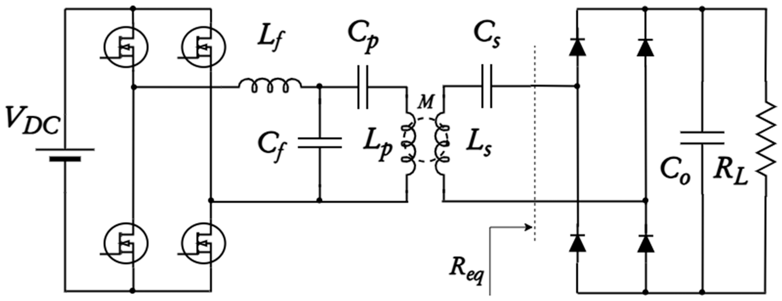
The wireless resonant converter considered in this work is an LCC-S topology. The electric scheme of this converter is shown in
Figure 1.
As can be seen in
Figure 1, the considered DC-DC converter is made by the combination of a DC-AC converter (V
DC as DC voltage source and MOSFETs full-bridge), a LC filter (typically called resonant tank) and an AC-DC converter (diode bridge and output filter capacitance
Co). The inductances
Lp and
Ls are associated with the coils that realize the wireless power transfer. Since the coils are in air, the coupling coefficient between these inductances is typically low; for this reason, some capacitors are generally added in wireless converters to reduce the reactive power generated by the wireless coils. The simplest configuration for wireless converters adopts two capacitances in series with
Lp and
Ls. The resulting converter topology is called Series-Series (SS) compensation. Although the simplicity of the SS topology makes it a frequently adopted converter for wireless power transfer, there are some limitations to take into account: limited freedom in the design of the converter and a limited range of output voltage achievable (it can behave just like buck converter) [
31,
32]. For this reason, according to specific applications, the adoption of more complex topologies could be required. The LCC-S compensation can overcome the limitations of the SS one, giving the possibility to work as a boost converter with a proper selection of the filter inductance
Lf. Concerning the modeling of resonant converters, the typical approach adopted in the literature is the so-called First Harmonic Approximation (FHA), where the input voltage is approximated with its fundamental harmonic. This approximation is valid when the converter’s working frequency corresponds to its natural resonant frequency. In this condition, independently by the nature of the input voltage waveform (square, PWM, trapezoidal, …), the combination of inductances and capacitances in the circuit behaves like a band-pass filter, which results in a short circuit for the fundamental harmonic and in a big impedance for high-frequency harmonics. In addition, under the FHA hypothesis, the AC-DC part of the converter can be modeled with an equivalent resistance
. This expression can be derived as the ratio between voltage and current before the rectifier, both written as functions, respectively, of the voltage and current on the load (detailed steps in [
33]).
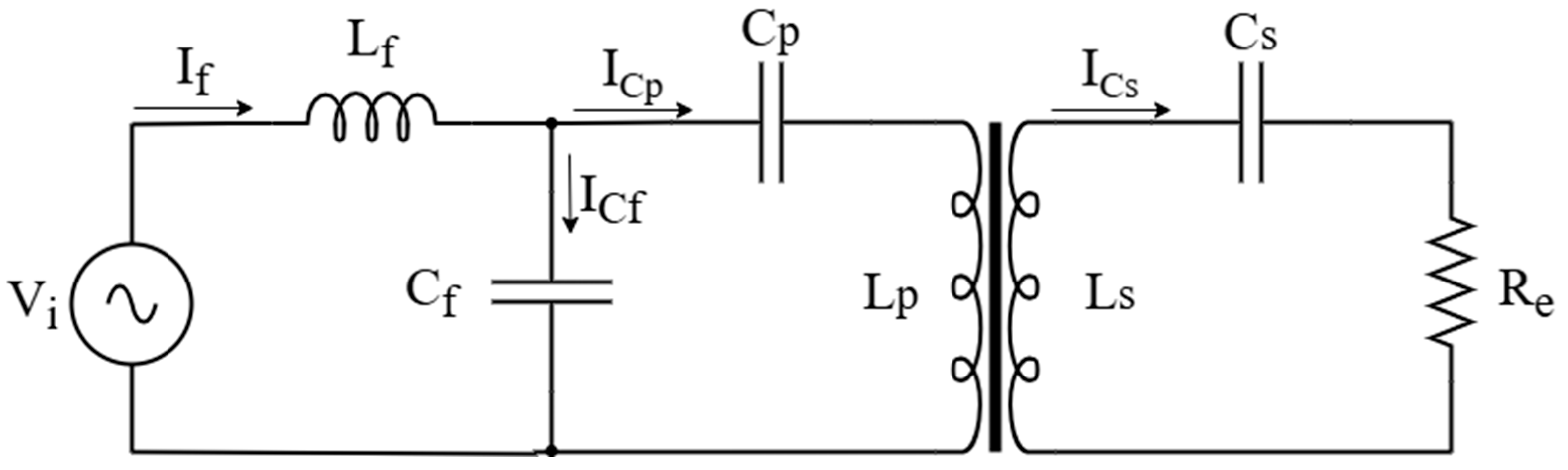
With these considerations, the converter in
Figure 1 can be simplified with the equivalent circuit in
Figure 2.
In this way, the converter model in steady-state conditions can be derived in frequency domain using phasors. Applying the Kirchhoff’ equations to the circuit in
Figure 2 the model of the LCC-S circuit can be easily derived in matrix form as follows:
where
r is a parasitic resistance associated with the inductive and capacitive components.
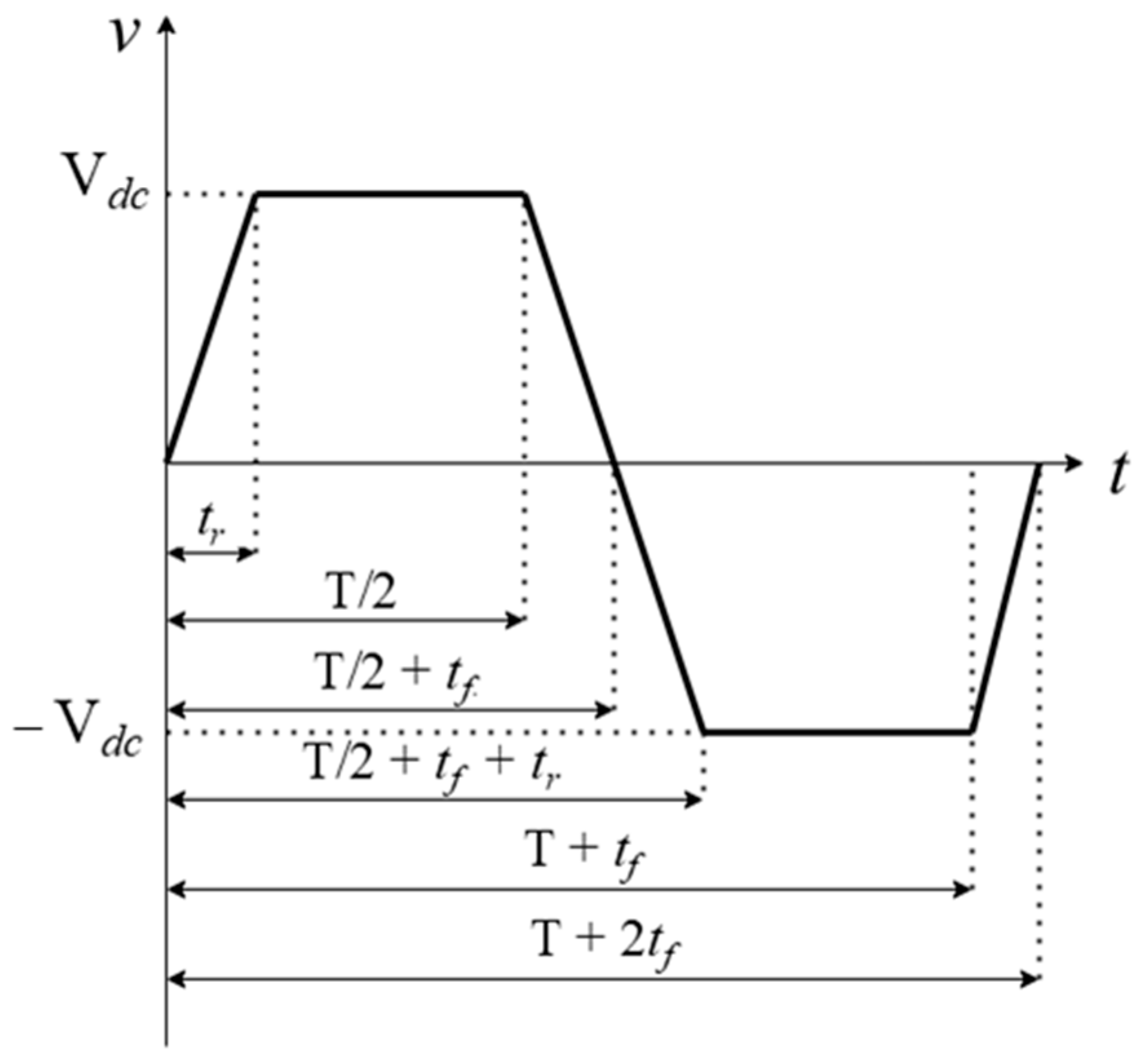
is the rms value of the input voltage. Since the input voltage has a trapezoidal waveform, its first harmonic can be evaluated using Fourier Transform. Considering the trapezoidal waveform in
Figure 3, where
tr and
tf are, respectively, the rise time and the fall time of MOSFETs, its time-domain function can be written as follows:
The first harmonic can be written as
Vs and
Vc are the Fourier coefficients, which can be evaluated as follows:
Developing the integrals, the following is obtained:
where
With
and
. Finally, the expression of
Vi phasor can be derived as follows:
In this work, a full-bridge inverter has been considered to supply voltage in the converter. Furthermore, a half-bridge inverter could also be considered. In this case, (3) has to be changed, putting
v(
t) = 0 when
. Consequently, terms s
4-s
7 and c
4-c
7 will be zero. In the next section, the way to evaluate
tr and
tf using the MOSFET datasheet will be shown. A last, but important consideration about this model concerns the dead time. The dead time is a parameter required in the DC-AC part of converters. It is a time interval, and all the switches in an inverter are open to avoid internal short circuits. Dead time can be included in a similar way to the model reducing by
td/2 (where
td is the dead time) the interval time where the
v(
t) function is equal to
VDC and −
VDC. Is has to be considered that by increasing the dead-time value, the resulting input voltage waveform becomes quite different from the ideal one; the result is an increase in the harmonics of the voltage and current waveforms, which could make FHA not valid anymore. To take into account several harmonics in the model of a resonant converter, the approaches presented in [
34,
35] can be applied, where each harmonic is studied considering a specific resistive–reactive equivalent load (instead of
Re). Otherwise, methods to directly eliminate the dead-time effects have also been proposed in the literature; they mainly consist of the usage of compensating circuits or devices [
36,
37].
3. MOSFET Circuital Model
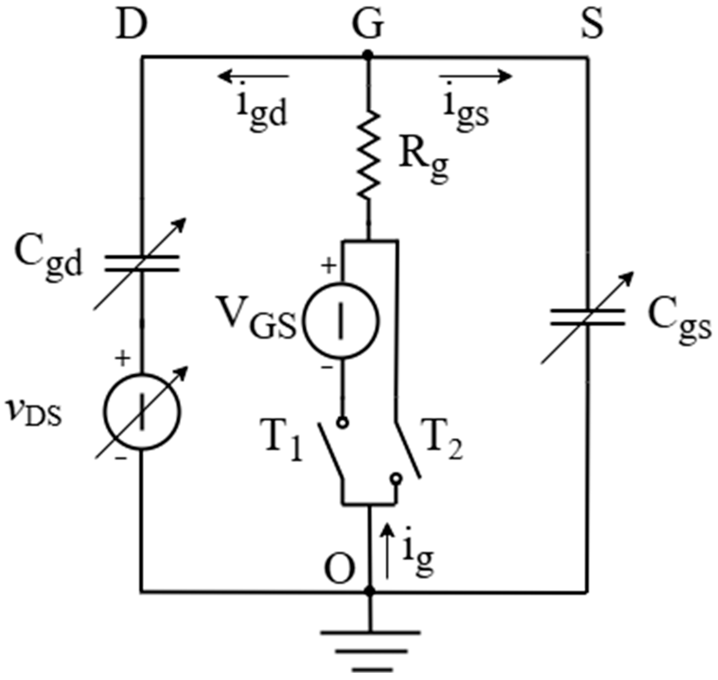
The circuital model in
Figure 4 represents the MOSFET gate. It is inspired by [
38,
39,
40]. The main idea of this circuit is to represent the transients of MOSFET during commutations, taking into consideration only two capacitances, which represent the amount of electric charge between the gate and, respectively, the drain and source. The simplicity of this approach is particularly suitable for the aim of this work, which is the proposal of a tool to easily evaluate the impact of MOSFET behavior in the converter performances.
The drain, gate and source of a MOSFET are modeled by, respectively, the left branch, the central branch and the right branch.
vDS is the voltage between MOSFET drain and source; it is modeled as a variable voltage source since its value changes during commutations between V
DC and 0 (neglecting the contribution of internal parasitic resistances).
Cgd and
Cgs are capacitances between, respectively, the drain and gate and the gate and source. They model the amount of charge in the MOSFET junctions, and they are functions of
vDS voltage. V
GS is the voltage imposed between gate and source to activate (or deactivate) the MOSFET. Finally,
Rg is the gate resistance. Typically, it can be written as
.
Rg(int) is the intrinsic resistance in the transistor chip: it is the real part of the electric impedance between the gate and source terminals, measured at 1 MHz, with an open drain terminal [
41].
Rg(ext) is an external resistance added in the gate drive circuitry to limit the oscillations of voltage and current in the MOSFET during commutations. T
1 and T
2 are ideal switches to consider the ON and OFF states of a MOSFET. When T
1 is closed and T
2 is open, a gate signal is provided and the MOSFET is activated. Conversely, when T
1 is open and T
2 is closed, the MOSFET is deactivated. As can be seen, no parasitic inductances are considered in the circuit to preserve the simplicity of the model. However, according to [
42,
43], at very high frequency, the drain series MOSFET inductance could be similar to
Lf. For this reason, in the next section we will show how to take into account this component in the converter model. The value of these inductances is typically very low, and their neglection make the analysis of the circuit very easy. Indeed, as it will be shown in the next lines, the evaluation of rise and fall times will require the consideration of just one capacitance.
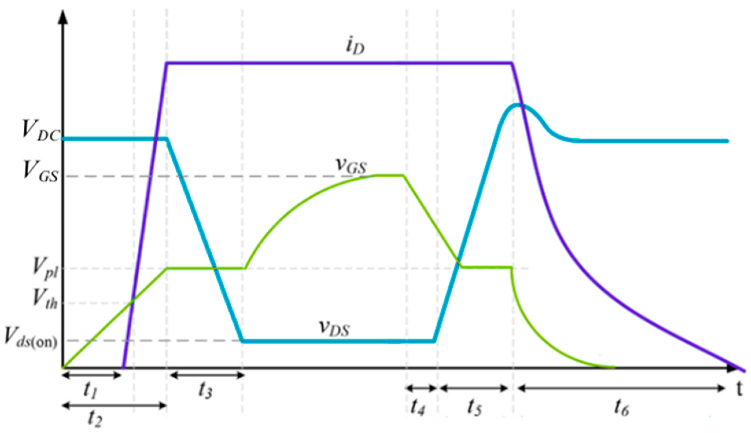
The origin of rise and fall times can be understood by observing the qualitative trend of drain–source voltage, GO voltage (with reference to
Figure 4) and drain–source current during commutations. They are reported in
Figure 5.
When a gate signal is provided (T
1 closed, T
2 open), the drain–source voltage starts to decrease after a delay (
t2-
t1 in the figure). In this time, the current provided by the gate charges the
Cgs capacitance. This is because the nominal value of
Cgs is normally higher than the
Cgd one, so the current mainly flows in
Cgs. As consequence, the value of drain–source voltage remains quite constant, and also the values of
Cgs and
Cgd are constant. When the
Cgs capacitance is charged, it imposes the electric potential in the A node in
Figure 4; the GO voltage stays constant (it is called a Miller Plateau), the current flows just on
Cgd and the
vDS voltage starts to decrease. After the
t3 time, the MOSFET is completely closed:
vDS is ideally zero (in
Figure 5 it is not zero due to the internal resistance of the MOSFET) and the drain–source current reaches its nominal value. The GO voltage increases until V
GS (voltage imposed between gate and source); the capacitances are constant (
vDS is constant), but with a different value compared with the initial one, so the current flows in both the capacitances. When the gate signal is removed (T
1 open, T
2 closed), an analogue situation occurs. As can be seen, the major losses in commutations are during
t3 and
t5, which will be considered in this work as the unique responses of, respectively, rise time and fall time. Note that the trends reported in
Figure 5 are referred to a MOSFET alone; they have been shown to explain the phenomena which occur, in general, during commutations. For the LCC-S converter considered in this work, the situation, in terms of waveforms, is different since the current has a periodic trend and it does not reach a constant value. Below, the procedure to analytically evaluate rise time and fall time will be shown.
During
t3, according to the considerations made in the previous lines, the currents are
and
. Considering
Figure 4, the equations referred to circuit are as follows:
Substituting (12) in (11), the following is obtained:
The derivative term
, according to
Figure 5, can be written as
(under the hypothesis that, when the MOSFET is in ON state,
vDS = 0). Finally, the expression of
t3 can be derived as follows:
In analogue way, but under the condition T
1 open, T
2 closed, the expression of
t5 can be derived:
The last consideration is that, as previously said,
Cgd is a function of
vDS, which varies both during
t3 and
t5. For this reason, it is commonly accepted to divide the gate charge
QGD stored during the Miller Plateau by the voltage swing seen on the drain connection. According to
Figure 5, the voltage swing can be approximated as V
DC; in this way, the final relationships for rise and fall times can be derived:
The values of the quantities reported in (16) can be found in the MOSFET datasheet. Note that in general, rise and fall times are directly reported in the datasheets, but they are provided for a specific set of working conditions (Rg, VGS, Vgp), and when they vary, the times also need to be updated. The results of this section allow us to run the proposed model of the converter, supposing an input voltage with a trapezoidal waveform instead of square one due to the rise and fall times of MOSFETs. This model will be compared in the next section with the performances of the converter in Simulink environment, where the real behavior of MOSFETs can be reproduced.
In
Figure 6, a flowchart which sums up the main steps required to reproduce the proposed model is presented.
4. Discussion
In this section, the performances of the proposed model are compared with simulations performed in the Simulink environment.
The design of a resonant converter is typically performed by selecting the values of the inductances and the desired resonant frequency. Then, capacitors are designed to resonate with the inductances. For LCC-s converter, the capacitors can be designed as follows:
In
Table 1, the electric features of the LCC-s converter are reported.
A standard in high-frequency Wireless Power Transfer is 6.78 MHz [
44,
45]. At this frequency, inductances can be easily realized in air, so switching losses are mainly responsible for the performance drop in the converter. The working frequency has been set near, but not exactly, in resonant conditions. In this way, the output voltage is a function of the load resistance (while in resonance the output voltage value is independent by the load); at the same time, FHA can be still applied since
fsw is very similar to
fo. A high coupling coefficient
k has been chosen (compared with the typical values for wireless power transfer). This can be assumed since, as can be seen in
Table 1, the inductances of the wireless coils are very low, so it is easy to stack them, limiting the stray magnetic field. These kinds of values can be achieved with very limited distances between coils (few millimeters), typical of the electronic devices’ charging applications [
46,
47]. Obviously, lower
k values need to be considered if other applications are taken into account. Note that the filter inductance
Lf can be easily realized in air (since the target value is very low).
The LCC-s converter has been reproduced in Simulink using Simscape library. The electric scheme is shown in
Figure 7.
The rectifier circuit has been reproduced with an equivalent resistance
Re. The neglection of the rectifier is allowed since this converter works near the resonance condition. In this way, it is possible to evaluate the impact of MOSFETs’ switching losses in the converter performances, which is the purpose of this work, without influences from other contributions. For the same reason, the parasitic resistances associated with the reactive components in the circuit have also been neglected. The MOSFETs have been reproduced using the N-Channel MOSFET block, which is programmed with the Shichman–Hodges model. This block gives the possibility to insert parameters directly taken from a datasheet. In particular, the transients during MOSFET commutations are reproduced using the values of parasitic capacitances provided in the datasheet. Producers typically provide the functions of parasitic capacitances with
vDS. These functions can be inserted in the N-Channel MOSFET block as look-up tables. Concerning instead the proposed models, the MOSFETs’ transients are reproduced evaluating the rise and fall times as shown in
Section 3. Two commercial MOSFETs have been taken in consideration, a IPPB009N03L from Infineon and a PSMN1R440YLD from Nexperia (datasheets available in [
48,
49]), to compare their impact on converter performances. With the values provided in the datasheets and reported in
Table 2, rise and fall times for the two MOSFETs can be evaluated with (16).
Considering the parameters in
Table 2, the following times are evaluated:
tr = 22.5 ns and
tf = 12.4 ns for IPPB009N03L,
tr = 24.48 ns and
tf = 16.32 ns for PSMN1R440YLD. According to these values, it is expected to find worse performances using PSMN1R440YLD. In
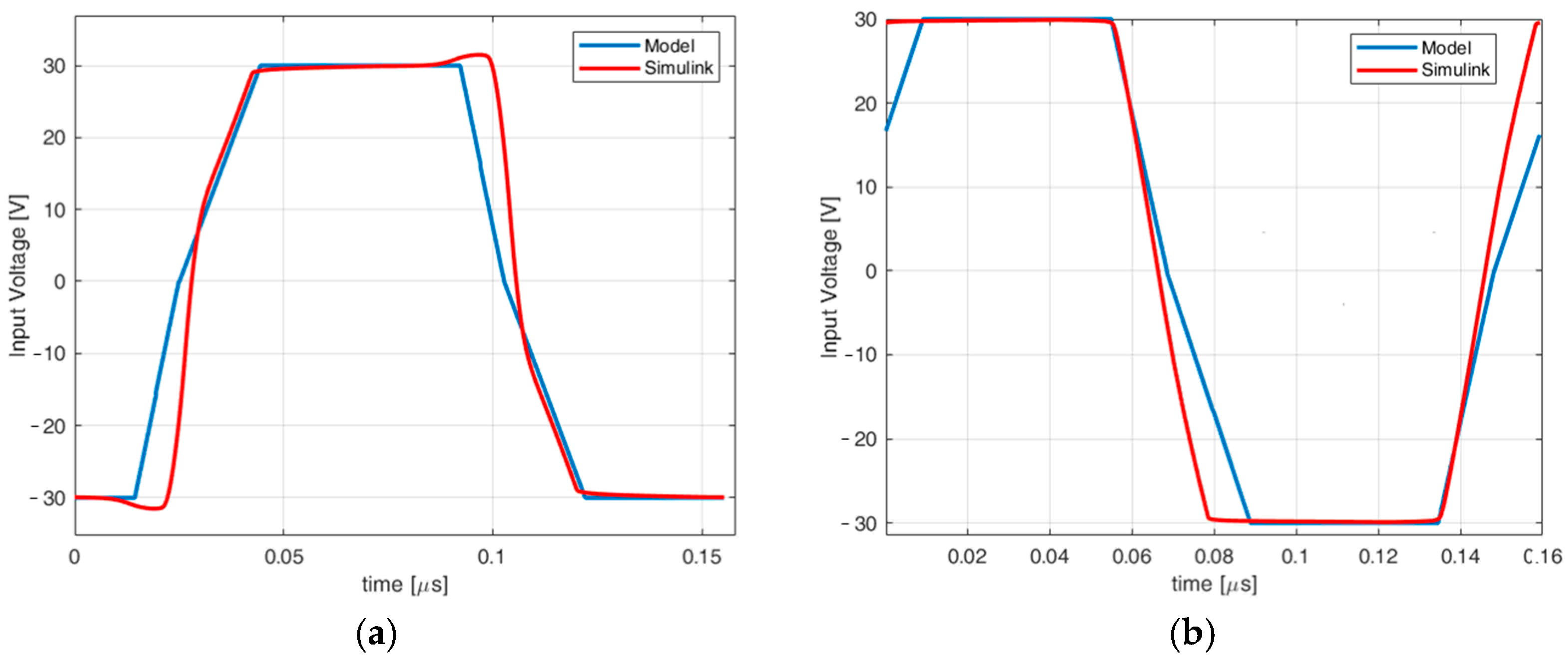
Figure 8, the input voltage evaluated as a trapezoidal function is compared with the input voltage provided by the MOSFET full-bridge reproduced in the Simulink environment.
The waveforms are slightly different; this is due to the different calculation process, which is very simplified in the case of the trapezoidal waveform, and for this reason much easier to be elaborated from the computational point of view. The proposed converter model takes in account, as discussed in
Section 2, the first harmonic of the blue waveforms in
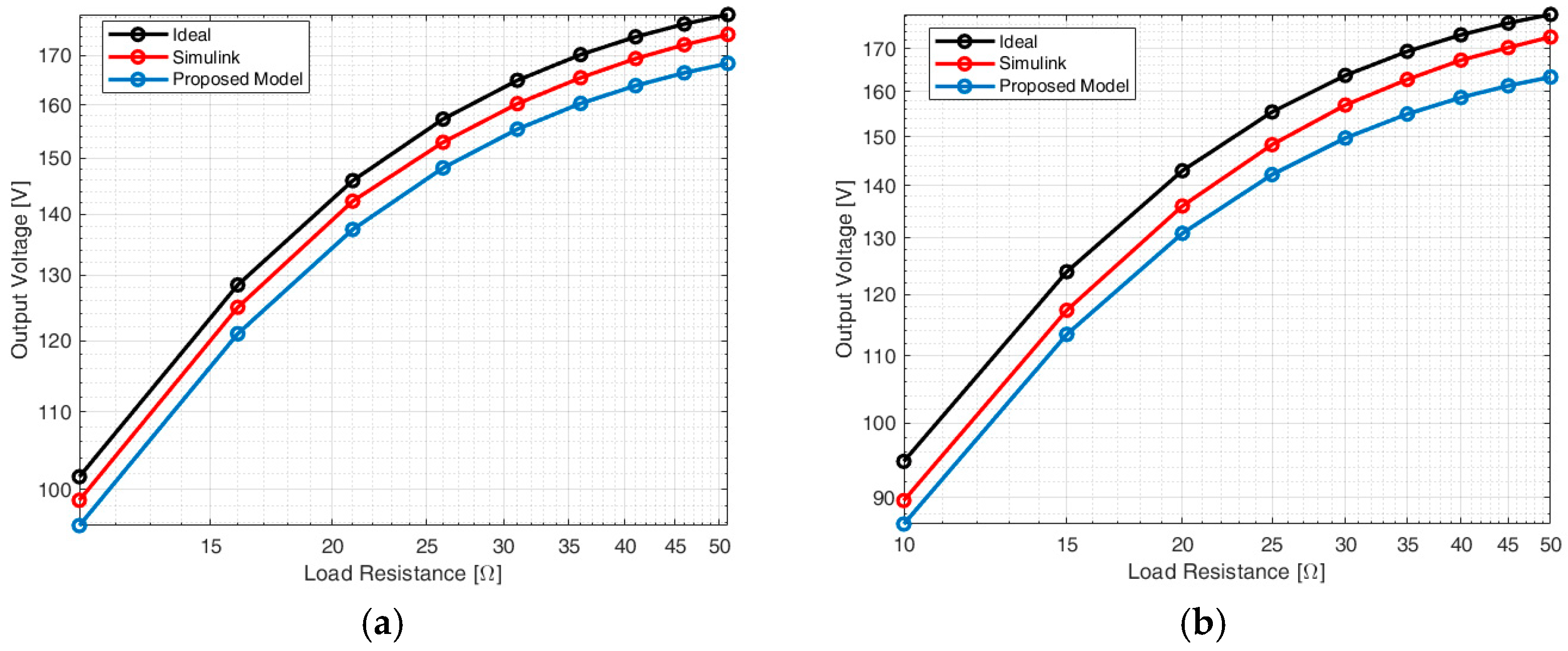
Figure 8. The performances of the proposed model are compared with Simulink evaluating in both cases the impact of MOSFETs’ behavior on the converter output voltage. The results are compared with the output voltage, theoretically achievable by the converter considering ideal switches; to obtain these values, the same model presented in
Section 2 has been adopted, imposing a pure square wave input voltage. The comparisons among models have been performed considering different input voltage and load resistance values. The following ranges have been considered: 10 V–30 V for the input voltage (recommended MOSFET working range according with producers) and 10 Ω–50 Ω for the load resistance. Results are presented in
Figure 9 and
Figure 10.
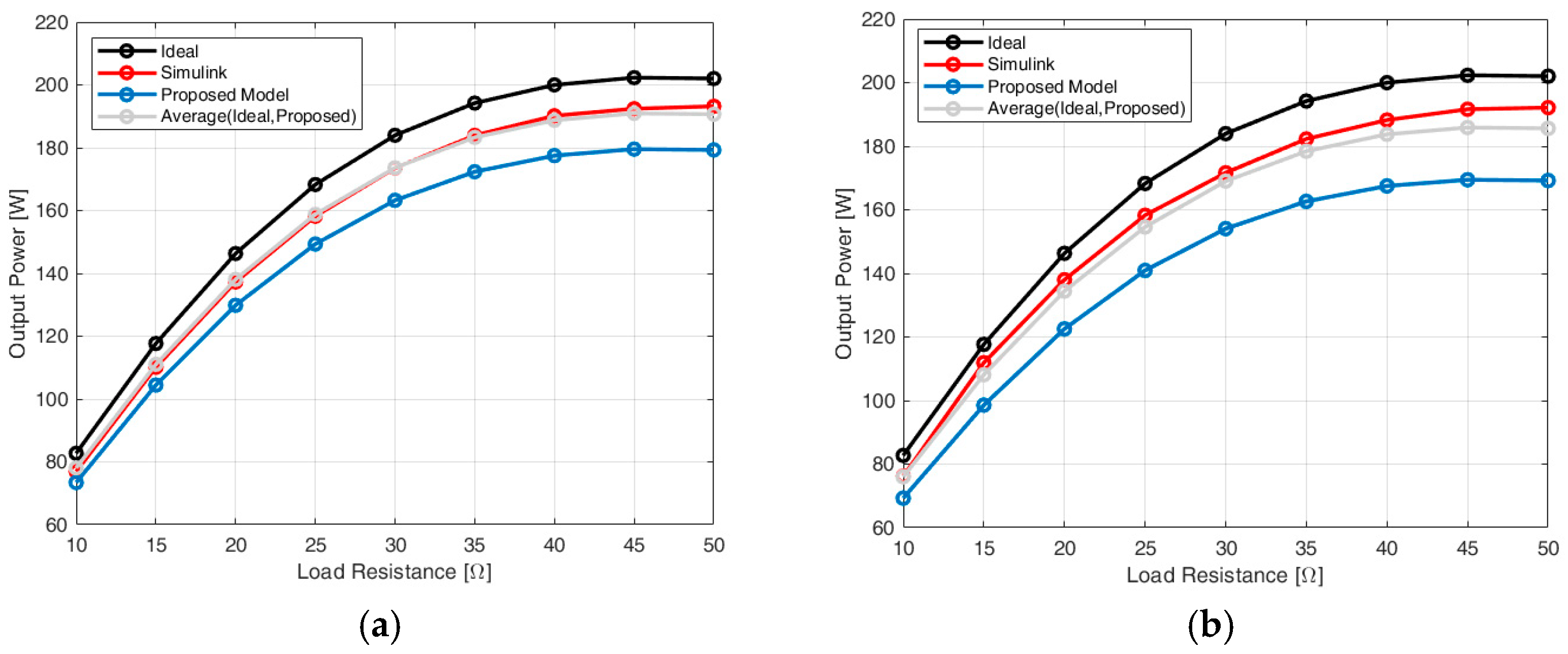
Several considerations can be made observing these results. First of all, the impact of the MOSFETs’ behavior on the converter performances is more important, as can be expected, when the current in the circuit increases. Indeed, the Simulink values are nearer to the ones of the proposed model when the input voltage increases, as shown in
Figure 9 (particularly highlighted in
Figure 9b, coherently with the expectations) and for low resistance values, as shown in
Figure 10 (more evident in
Figure 10b, coherently again with the expectations). Secondly, the values predicted with the proposed model are very similar to the ones calculated in Simulink; with reference to
Figure 10, the percentage error between model and Simulink is always under 3.5% in
Figure 10a and under 5.5% in
Figure 10b. Finally, the proposed model realizes a slight underestimation of the results. This means that, considering Simulink as the most reliable value, using the ideal model and the proposed one, the range containing the real output voltage value can be defined, and an estimation of the real value could be performed, as first approximation, as the average of the black and blue trends in
Figure 9 and
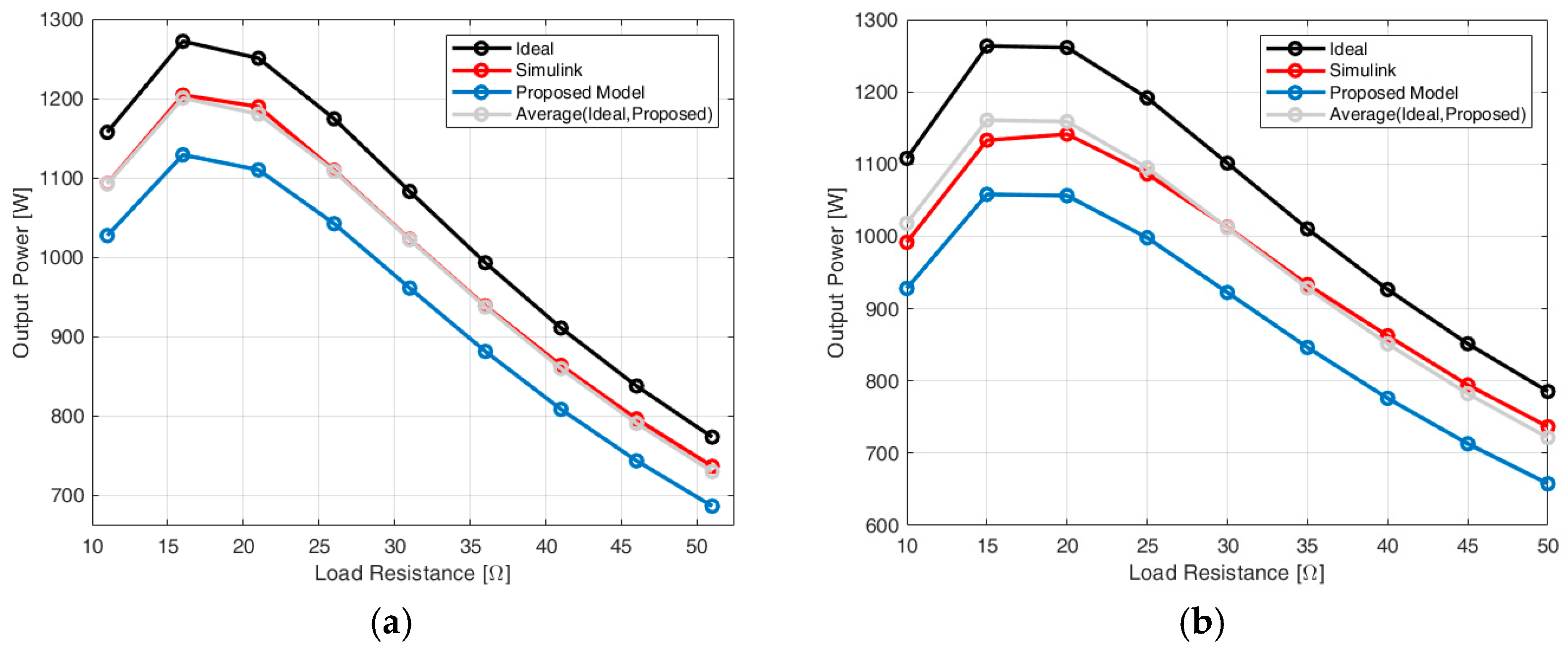
Figure 10. To verify that, the output power calculated with the different discussed models is reported in
Figure 11. In addition, the average between ideal and proposed model has been evaluated.
As can be seen, the prediction made by averaging the ideal and the proposed models is almost superimposed with the Simulink trend. So, the combination of these two models allows for exploring lots of working conditions (different input voltages and loads) in a paltry computational time (fractions of seconds) and granting reliable results. As a last consideration, observing the trends in
Figure 11, the maximum power achievable, according to Simulink, is 1.2 kW in
Figure 11a and 1.14 kW in
Figure 10b; in correspondence of these values, the ideal model predicts, respectively, 1.27 kW and 1.26 kW. The MOSFET switching losses cause a 5.8% output power drop using IPPB009N03L and a 10.5% output power drop using PSMN1R440YLD, confirming the expectations. Furthermore, these results underline once again the importance of the proposed model for a preliminary evaluation of the impact of electronic devices in the converter performances since the differences in the final results can be anything but negligible. As anticipated in the previous section, the drain series MOSFET inductance can have a value similar to
Lf. In the datasheet of MOSFETs considered in this work, the values of parasitic inductance are not reported. In addition, according to [
42,
43], a value of about 20 nH can be assumed. This inductance can be included in the proposed converter model by adding an inductance
Lmos in series with
Lf.
Lmos can be evaluated as the double of the drain series MOSFET inductance, since, with a full-bridge inverter, two MOSFETs are in conduction in each half-period. So, considering an
Lmos inductance of 40 nH, a comparison in terms of output power with Simulink and our proposed model has been performed. Results are provided in
Figure 12 for the two kinds of MOSFET as functions of the load resistance.
As can be seen, this inductance has a non-negligible effect in the converter performances (output power is significantly lower compared with
Figure 11) because, for this particular converter topology, the performances are strictly influenced by the value of the filter inductance (that, in this case, is the series between
Lmos and
Lf). Furthermore, the proposed approach, averaged with the ideal model, can still predict results very similar to Simulink.
Finally, a discussion on how to estimate MOSFET losses with the proposed model can be conducted. In particular, conduction losses can be calculated putting in series with the
Lf inductance a resistance equal to the double of the drain–source MOSFET resistance (
RDS): this is because two MOSFETs are in conduction, in a full-bridge inverter, for each half-period. Switching losses can be evaluated as the double (for the same reason of conduction losses) of the average power, in one period, between the current in the
Lf inductance and the linear strokes of the trapezoidal input voltage. In parallel, in Simulink, the average power in one period between voltage and current across the MOSFET represents the total loss in the device (switching and conduction); the total losses in the inverter can be obtained multiplying by four the losses on the single MOSFET. The two contributions can be split by evaluating conduction losses as the average power on the RDS MOSFET resistance, so the switching losses will be the difference between total losses and conduction losses. In addition, we performed some tests in Simulink, and then we saw that conduction losses are extremely lower than the switching one (as also expected in the literature); indeed, it has to be considered that the
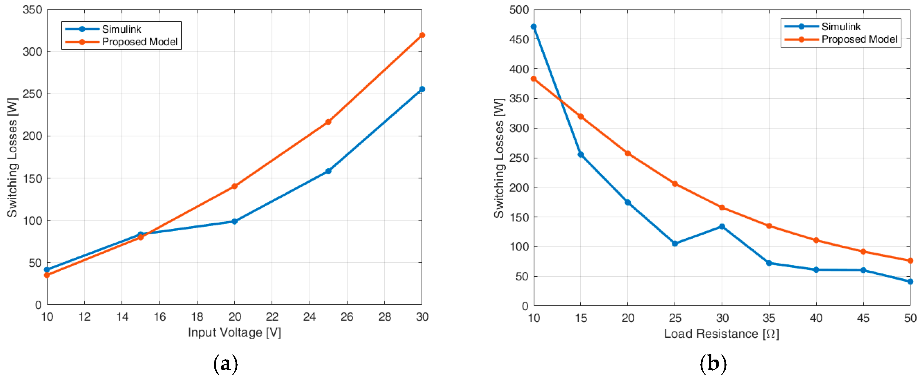
RDS resistance is very low: 0.95 mΩ for IPPB009N03L MOSFET and 1.6 mΩ for PSMN1R440YLD MOSFET. So, the attention can be focused just on switching losses. Considering the IPPB009N03L MOSFET, the comparison of switching losses calculated using Simulink and the proposed model as function of input voltage and load resistance is shown in
Figure 13.
As can be seen, the two approaches provide similar results. This kind of analysis can be exploited to evaluate not only the performances of MOSFETs, but also the resulting global efficiency of the converter.


