Article

Reduced-Order Nonlinear Envelope Modeling and Simulation of Resonant Inverter Driving Series Resistor–Inductor–Capacitor Load with Time-Varying Component Values

Applied Energy Laboratory, School of Electrical and Computer Engineering, Ben-Gurion University of the Negev, Beer-Sheva 8410501, Israel
*
Author to whom correspondence should be addressed.
Appl. Sci. 2025, 15(8), 4502; https://doi.org/10.3390/app15084502
Submission received: 20 February 2025 / Revised: 10 April 2025 / Accepted: 10 April 2025 / Published: 18 April 2025
(This article belongs to the Special Issue New Insights into Wireless Power Transmission Systems)

Abstract

:
Envelope modeling is an efficient way to obtain the large-signal amplitude and phase dynamics of fast-varying sinusoidal signals required for, e.g., resonant frequency tracking or energy transfer rate regulation in power converters. In addition, the method eliminates fast-varying parameters from the model so that the simulation time and memory requirements are reduced. This paper reveals the envelope-modeling process of a capacitor-powered resonant inverter feeding a time-varying series RLC load, often employed in pulsed-power applications. Such an arrangement is nontrivial since the system does not reach a steady state within a single pulse duration. Furthermore, model order reduction is carried out without performing linearization due to large variations in the expected operation point. As a result, a reduced-order nonlinear envelope model is derived and validated by simulations. Both the proposed modeling method and the derived model aim to simplify the challenging task of feedback controller design.

1. Introduction

The need for resonant converters is prominent in the field of induction heating in the metal industry [1], domestic induction cooking [2], and pulsed-power plasma applications [3]. Magnetic levitation systems for a variety of transportation solutions [4], wireless power supplies/chargers for electric vehicles [5,6], cellphones [7], and biomedical implants [8] are also based on resonant conversion. A typical resonant power delivery system utilizes an inverter (or DC–AC converter [9,10]) to create an alternating-current (AC) flow through a coil for the generation of alternating magnetic flux, inducing a voltage across a secondary coil or workpiece [11,12]. The equivalent load “seen” by the inverter may be represented by a series resistor–inductor (RL) arrangement, as shown in Figure 1a [13]. In this model, the energy transferred to the load is represented by the equivalent resistance R, while the equivalent inductance L reflects the magnetic behavior of the system. Typical resonant converters operate at relatively high switching frequencies ωs (several tens of rad/s up to several Mrad/s). As a result, the equivalent inductance impedance sL limits the amount of power transferred to the load by increasing the impedance of the equivalent load “seen” by the inverter to |Zeq,a(ωs)| = (R2 + (ωsL)2)0.5.
To overcome this limitation, a common solution is adding a resonant capacitor C in series with the coil, as shown in Figure 1b [14]. As a result, the equivalent load impedance “seen” by the inverter becomes |Zeq,b(ωs)| = (R2 + (ωsL − 1/ωsC)2)0.5 so that the inductance contribution is offset by that of the capacitance. If | ωsL − 1/ωsC| < ωsL, then |Zeq,b(ωs)| < |Zeq,a(ωs)|, and the power transferred to the load by the same inverter increases.
Another typical challenge in the process of resonant power delivery is the time-varying nature of equivalent resistance and/or inductance due to, e.g., workpiece state-of-matter changes in induction heating applications and load/coupling coefficient variations in wireless power transfer applications. In addition, the value of the resonant capacitor may also drift due to temperature variations, high-current-flow-induced mechanical stresses, and degradation [15]. As a result, the equivalent load impedance “seen” by the inverter varies (relatively slowly) during the process. Consequently, a feedback control system is employed to counteract these variations by adjusting the inverter’s operational state (output voltage and/or frequency) accordingly. This is successfully accomplished in long processes, such as metal processing and battery charging. However, the above-mentioned challenge is critical in pulsed-power applications [16], such as hydrogen fusion. In fusion systems, magnetic levitation and induction heating are simultaneously carried out during a process in which the hydrogen is rapidly heated to a high temperature by an intensive short-time (millisecond-order) power burst for gas-to-plasma conversion. In case energy delivery maximization is the goal, the impedance “seen” by the inverter should be minimized by keeping the system at resonance (forcing ωsL − 1/ωsC = 0, as shown in Figure 1b). Meanwhile, if it is desired to stabilize the power delivered to the load at a certain reference value, then the current (and, hence, |Zeq,b(ωs)|) should be regulated. However, the values of RLC network parameters are expected to vary due to the above-mentioned reasons. Therefore, the feedback control system must react very quickly (within the fraction of the power burst duration) to these changes by varying the operational frequency to restore the desired operation point.
Note that the discussion above is based on phasor-domain analysis, where the impedances are inductive and are mathematically expressed as functions of the operating frequency. Nevertheless, phasor-domain analysis is only valid for systems operating in a steady state (i.e., at constant magnitudes and phases) with constant-frequency sinusoidal excitation. Nonetheless, in short-pulsed-power applications (e.g., hydrogen fusion systems), the power burst duration is lower than the settling time of the system, so classical phasor-domain analysis is irrelevant. As an example, consider a constant-magnitude constant-frequency sinusoidal voltage v t = V M s i n ω s t applied to a series RLC network (temporarily considering non-varying parameter values for brevity), as shown in Figure 1b at t = 0. The current flowing through the network would then be given by i t = I M ( t ) s i n ω t t , as shown in Figure 2. In a steady state, the linear time-invariant nature of the system imposes i s s t = I M s s s i n ω s t + φ s s , with the constants I M s s = VM/|Zeq,b(ωs)|, φ s s = a r g Z e q , b ( ω s ) , and ω = ω s . However, the instantaneous current magnitude and frequency vary during the transient period so that I M ( t ) I M s s and ω t ω s . Meanwhile, the instantaneous current frequency may be expressed as ω t = ω s + ω ( t ) . Hence, the current flowing through the network may be expressed as i t = I M ( t ) s i n ω s t + φ t with φ t = ω ( t ) t so that the varying frequency is translated into a constant frequency with a varying phase, as shown in Figure 2. In practice, the inverter is switched off (in the given example) at 1 ms, while the system would have reached a steady state only around 2.75 ms. Consequently, classical phasor analysis considering a steady state is irrelevant for analyzing the system behavior within the power burst duration period (as mentioned above).
The switching-period-averaged power delivered to the RLC network in the example above is P(t) ≈ 0.5VMIM(t)cos(φ(t)). In case energy delivery maximization is the goal, then I M t cos φ t d t should be maximized by the controller over the power burst period. Alternatively, I M t cos φ t should be regulated by the controller over the power burst period if power stabilization is desired. In order to design suitable controllers for either case or both, a dynamic model linking system inputs with an instantaneous current magnitude and phase is necessary. It was demonstrated in [17] that phasor-domain analysis may also be applied to systems with slow-varying (rather than constant) magnitudes and phases. The approach is better known as “envelope modeling” [18], originating from the fact that the average power delivered to a load by a sinusoidal current is only determined by its magnitude (envelope) and phase, as shown by the average power equation above [19]. As a result, switching-frequency behavior may be disregarded since it is irrelevant for the average power transfer process (disregarding switching losses). Unfortunately, the major drawback of the envelope-modeling approach is probably the inherent system order augmentation (imposed by splitting each AC-side state variable into the corresponding magnitude and phase). The resulting high-order dynamic model of the plant complicates the controller design process so that model order reduction is beneficial [20].
Traditionally, reduced-order models [21] rely on linearization techniques to achieve simplification. However, such approaches are suitable for steady-state operating systems with small variations around the operation point while struggling to correctly capture the behavior of systems with significantly varying operation points (such as short-time pulsed-power applications). Another method to achieve a low-order envelope model based on the energetic coupling between the system inductance and capacitance was proposed in [22]. However, it is only valid in the close vicinity of the resonance. Consequently, a nonlinear reduced-order model capable of accurately capturing the system behavior under large signal variations is necessary. It must be emphasized that due to the extremely high current flow required for relatively short periods, pulsed-power applications in general, and fusion inverters in particular, are typically powered by pre-charged capacitor banks rather than constant-voltage sources [16]. Consequently, the inverter input voltage should be considered as an additional non-controllable state variable, increasing the overall system order while imposing the operational frequency to serve as the only controllable input to the system. When frequency control is adopted, operation in the inductive region is usually preferable as it allows attaining zero voltage switching, alleviating converter switch stresses and losses, thus enhancing the longevity and increasing the efficiency of the system [23]. Table 1 summarizes the modeling methods presented above, indicating their validity range and applicability.
Taking all the above into account, the nonlinear envelope-modeling process of a capacitor-powered resonant inverter driving series RLC load with time-varying component values is presented in this paper. First, a full-order envelope model is derived. Then, model order reduction is carried out under the assumption of a slow-varying amplitude derivative and phase (SVADP), as proposed in [21], yet without linearization, resulting in a novel nonlinear reduced-order envelope model, valid both at the resonance frequency and off-resonance. In order to demonstrate the validity of the proposed approach, the device-level switched model of the capacitor-powered resonant inverter driving series RLC load with time-varying component values and the corresponding reduced-order envelope model are simulated concurrently, and close matching between the outcomes is demonstrated under different operating conditions.
The rest of this paper is organized as follows. The system under consideration and basic assumptions are introduced in Section 2. The derivation of the full-order nonlinear system envelope model is carried out in Section 3. The proposed model reduction process is revealed in Section 4 and verified by simulations in Section 5. This paper is concluded in Section 6.

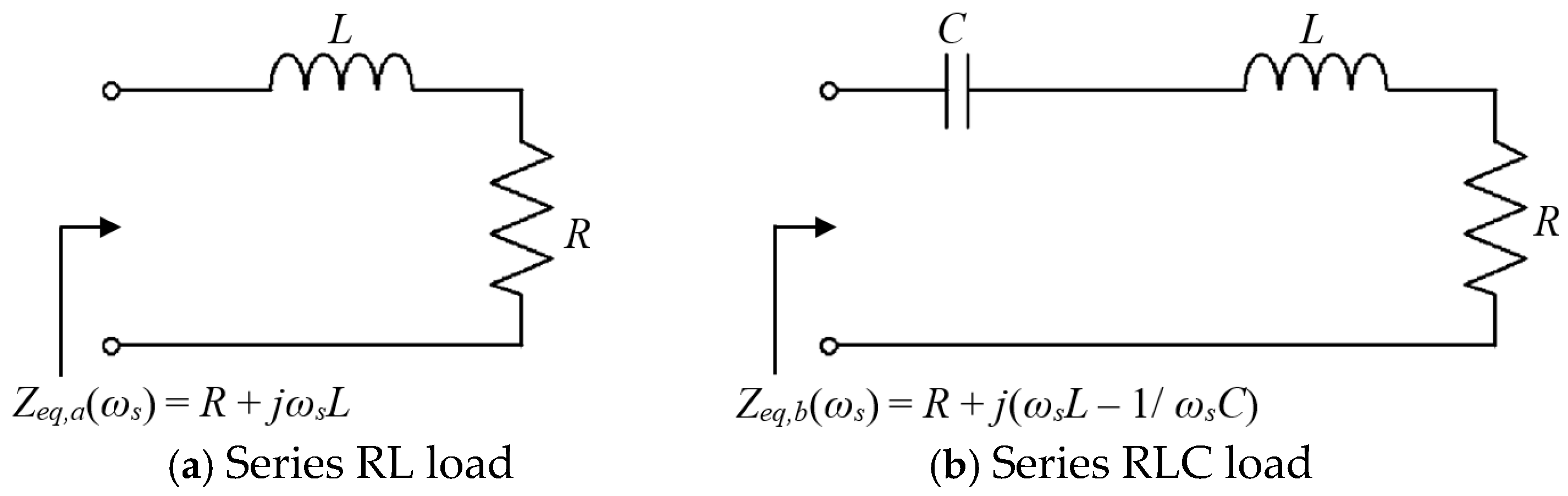
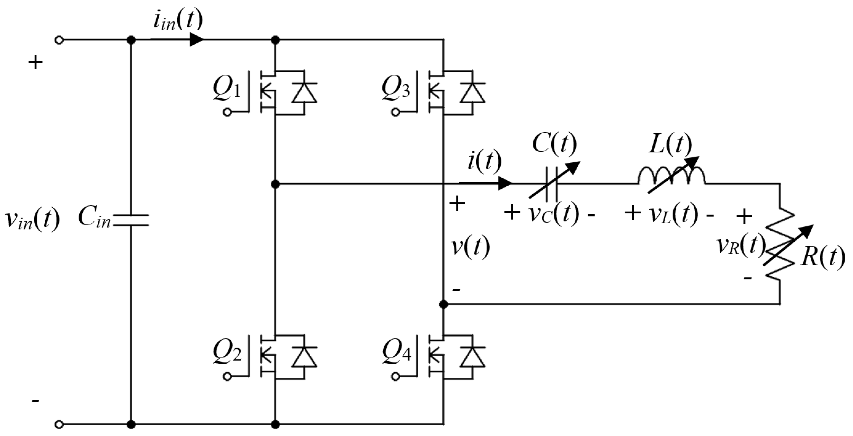
2. System Under Consideration and Basic Assumptions

A full-bridge inverter [24,25] feeding a generalized series-connected resistor–inductor–capacitor (RLC) network with time-varying component values [26], as shown in Figure 3, is considered in this work. Due to the nature of pulsed-power applications, the pre-charged DC-side capacitance Cin functions as the only system energy source within a single pulse period. The values of the RLC network components are assumed to vary in time according to
R ( t ) = R 0 + Δ R ( t ) Ω L ( t )   = L 0 + Δ L ( t ) H C ( t )   = C 0 + Δ C ( t ) F ,
where the first (zero-indexed) right-hand side term denotes the corresponding constant nominal value, and the second right-hand term signifies the matching time-varying quantity. In addition, the practical relative rate of change in R(t), L(t), and C(t) is significantly lower than the angular converter switching frequency ωs(t). Consequently, the RLC network component values would be considered constant over a single switching period Ts = 1/fs [s] with fs(t) [Hz] = ωs(t)/2 π . The DC-side capacitance Cin is assumed to be constant and known, pre-charged to an initial voltage of vin(0) = V0 prior to the pulse creation at t = 0. During operation, the DC-side capacitance discharges while providing energy to the resistance R(t). Nevertheless, the Cin is typically high enough to assume that the average value of vin(t) remains unchanged during a single switching period Ts. The converter switches operate in a complementary fashion with a duty cycle of 50% so that their output voltage v(t) may be approximated by the following square-wave within a single switching period:
v ( t ) = v i n ( t ) , 0 t T s ( t ) 2 v i n ( t ) ,   T s ( t ) 2 t T s ( t ) ,
where switch parasitics are neglected for simplicity. In addition, note that the converter switching frequency may vary in general, yet the corresponding relative rate of change is significantly lower than ωs(t).

3. Full-Order Envelope Model Derivation

The converter output voltage may be expressed as the sum of voltages across the individual RLC network elements (cf. Figure 3):
v ( t ) = R ( t ) i ( t ) v R ( t ) + v L ( t ) + v C ( t ) .
The voltages across the inductance and capacitance are related to the AC-side current i(t) as
v L ( t ) =   d L ( t ) i ( t ) d t =   d L ( t ) d t i ( t ) + d i ( t ) d t L ( t ) ,
and
i ( t ) =   d C ( t ) v C ( t ) d t =   d C ( t ) d t   v C ( t ) + d v C ( t ) d t C ( t ) ,
respectively. Meanwhile, v(t) may be described (cf. (2)) by the following Fourier series:
v ( t ) = n A n sin ω s ( t ) d t + θ n , A n = 4 v i n n π sin n π 2 .
In practical series resonant converters, the current is nearly-sinusoidal due to the high quality factor of the RLC network [27,28] so that the first inverter output voltage harmonic only is relevant to the power transfer. The inverter output voltage is replaced for the sake of envelope modeling by its first harmonic given by
v ( t )   v 1 ( t ) = A 1 ( t ) sin θ s ( t ) + θ 1 , θ s ( t ) = ω s ( t ) d t .
with (where the corresponding phase is used as the reference hereafter)
A 1 ( t ) = 4 v i n ( t ) π ,     θ 1 = 0 .
Consequently, the general expressions for the AC-side capacitor voltage and current are given by
v C ( t ) = V M ( t ) sin θ s ( t ) + φ v ( t ) = V M ( t ) cos φ v ( t ) sin θ s ( t ) + V M ( t ) sin φ v ( t ) cos θ s ( t )
and
i ( t ) = I M ( t ) sin θ s ( t ) + φ i ( t ) = I M ( t ) cos φ i ( t ) sin θ s ( t ) + I M ( t ) sin φ i ( t ) cos θ s ( t ) ,
respectively [29], where VM(t) and IM(t) stand for the corresponding magnitudes, and φv(t) and φi(t) symbolize the corresponding phases, denoting
V M ( t ) cos φ v ( t ) v C s ( t ) ,     V M ( t ) sin φ v ( t ) v C c ( t ) ,
and
I M ( t ) cos φ i ( t ) i s ( t ) ,     I M ( t ) sin φ i ( t ) i c ( t ) ,
Equations (9) and (10) may be rewritten as
v C ( t ) = v C s ( t ) sin θ s ( t ) + v C c ( t ) cos θ s ( t )
and
i ( t ) = i s ( t ) sin θ s ( t ) + i c ( t ) cos θ s ( t ) ,
respectively. The time-domain derivatives of (13) and (14) are then, respectively, given by
d v C ( t ) d t = d v C s ( t ) d t ω s ( t ) v C c t sin θ s ( t ) + d v C c ( t ) d t + ω s ( t ) v C s t cos θ s ( t ) ,
and
d i ( t ) d t = d i s ( t ) d t ω s ( t ) i c ( t ) sin θ s ( t ) + d i c ( t ) d t + ω s ( t ) i s ( t ) cos θ s ( t ) .
Combining (13)–(16) with (3)–(5) and (7) yields
4 v i n ( t ) π sin θ s ( t ) = R ( t ) + d L ( t ) d t i s ( t ) sin θ s ( t ) + i c ( t ) cos θ s ( t ) + L ( t ) d i s ( t ) d t ω s ( t ) i c ( t ) sin θ s ( t ) + L ( t ) d i c ( t ) d t + ω s ( t ) i s ( t ) cos θ s ( t ) + v C s ( t ) sin θ s ( t ) + v C c ( t ) cos θ s ( t )
and
i s ( t ) sin θ s ( t ) + i c ( t ) cos θ s ( t ) = d C ( t ) d t v C s ( t ) sin θ s ( t ) + v C c ( t ) cos θ s ( t ) + C ( t ) d v C s ( t ) d t ω s ( t ) v C c ( t ) sin θ s ( t ) + d v C c ( t ) d t + ω s ( t ) v C s ( t ) cos θ s ( t ) ,
respectively. Separating (17) and (18) into sine and cosine terms gives
4 v i n ( t ) π sin θ s ( t ) = R ( t ) + d L ( t ) d t i s ( t ) sin θ s ( t ) + L ( t ) d i s ( t ) d t ω s ( t ) i c ( t ) sin θ s ( t ) + v C s ( t ) sin θ s ( t ) , ,
0 = R ( t ) + d L ( t ) d t i c ( t ) cos θ s ( t ) + L ( t ) d i c ( t ) d t + ω s ( t ) i s ( t ) cos θ s ( t ) + v C c ( t ) cos θ s ( t ) ,
and
i s ( t ) sin θ s ( t ) = C ( t ) d v C s ( t ) d t ω s ( t ) v C c ( t ) sin θ s ( t ) + d C ( t ) d t v C s ( t ) sin θ s ( t ) ,
i c ( t ) cos θ s ( t ) = C ( t ) d v C c ( t ) d t + ω s ( t ) v C s ( t ) cos θ s ( t ) + d C ( t ) d t v C c ( t ) cos θ s ( t ) ,
respectively. Equating the coefficients at both sides of each equation, a set of four envelope dynamics equations with corresponding general initial conditions is established as [30,31]
d i s ( t ) d t = ω s ( t ) i c ( t ) + 1 L ( t ) 4 v i n ( t ) π R ( t ) + d L ( t ) d t i s ( t ) v C s ( t ) ,     i s ( 0 ) = I 0 s ,
d i c ( t ) d t = ω s ( t ) i s ( t ) 1 L ( t ) R ( t ) + d L ( t ) d t i c ( t ) + v C c ( t ) ,   i c ( 0 ) = I 0 c
d v C s ( t ) d t = 1 C ( t ) i s ( t ) + ω s ( t ) v C c ( t ) d C ( t ) d t v c c ( t ) ,     v C s ( 0 ) = V C 0 s ,
d v C c ( t ) d t = 1 C ( t ) i c ( t ) ω s ( t ) v C s ( t ) d C ( t ) d t v C c ( t ) ,     v C c ( 0 ) = V C 0 c .
Moreover, the following holds, according to (11) and (12):
V M ( t ) = v C s ( t ) 2 + v C c ( t ) 2 ,
I M ( t ) = i s ( t ) 2 + i c ( t ) 2 ,
φ v ( t ) = arctan v C c ( t ) v C s ( t ) ,
φ i ( t ) = arctan i c ( t ) i s ( t ) .
In order to find the relation between the AC-side envelope dynamics described by (23)–(26) and the DC-side inverter voltage, note that the DC-side current and instantaneous power are given by
i i n ( t ) = C i n d v i n ( t ) d t
and
p i n ( t ) = v i n ( t ) i i n ( t ) = v i n ( t ) C i n d v i n ( t ) d t ,
respectively. In case of lossless conversion,
p ¯ i n ( t ) = p ¯ o u t ( t )
with
x ¯ ( t ) = 1 T s t t + T s x ( u ) d u
denote the average value of x(t) over Ts. The average output and input converter power are given by (cf. (10))
p ¯ o u t ( t ) = R ( t ) I M ( t ) 2 2
and
p ¯ i n t = v ¯ i n t C i n d v ¯ i n t d t ,
respectively. Equations (35) and (36) yield the input voltage dynamics given by
d v ¯ i n t d t = R t 2 v ¯ i n t C i n I M t 2 ,     v ¯ i n 0 = V 0
with the corresponding general initial condition. The set of state-space Equations (23)–(26) and (37) and output Equations (27)–(30) form a full (fifth-order) envelope model of the system [32]. The corresponding block diagram is depicted in Figure 4.

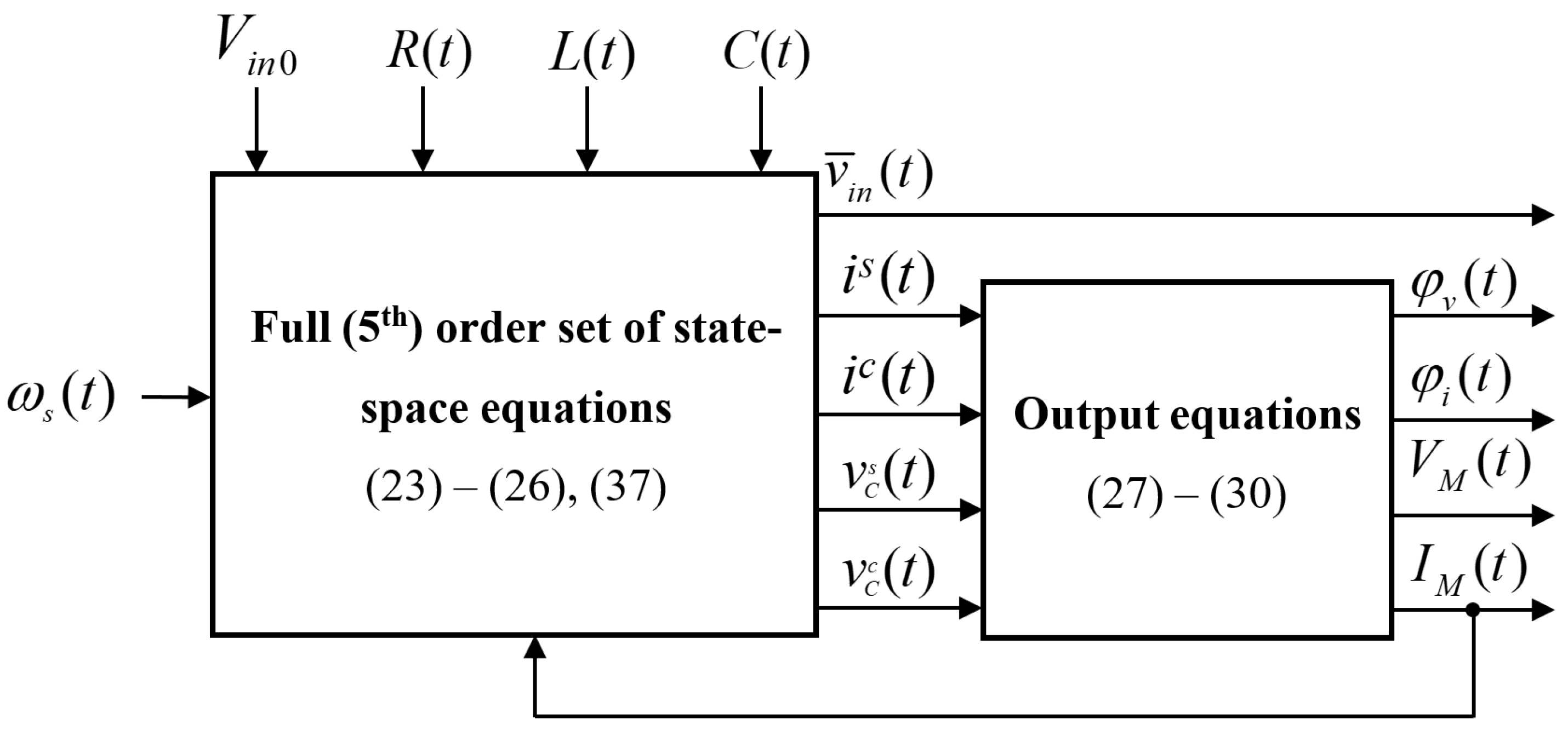
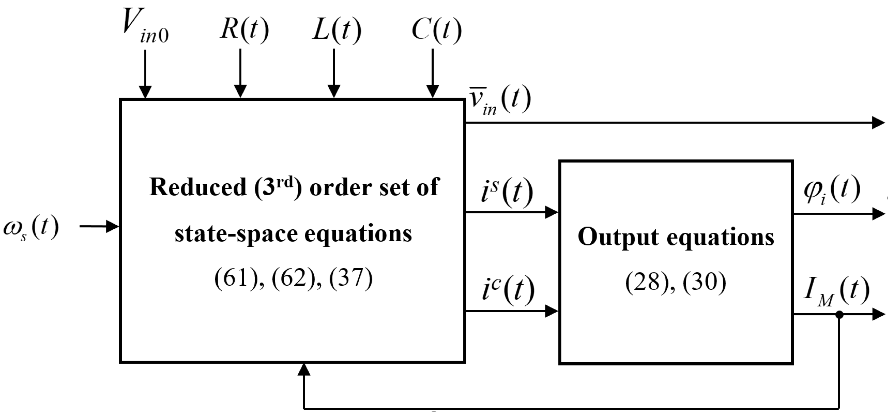
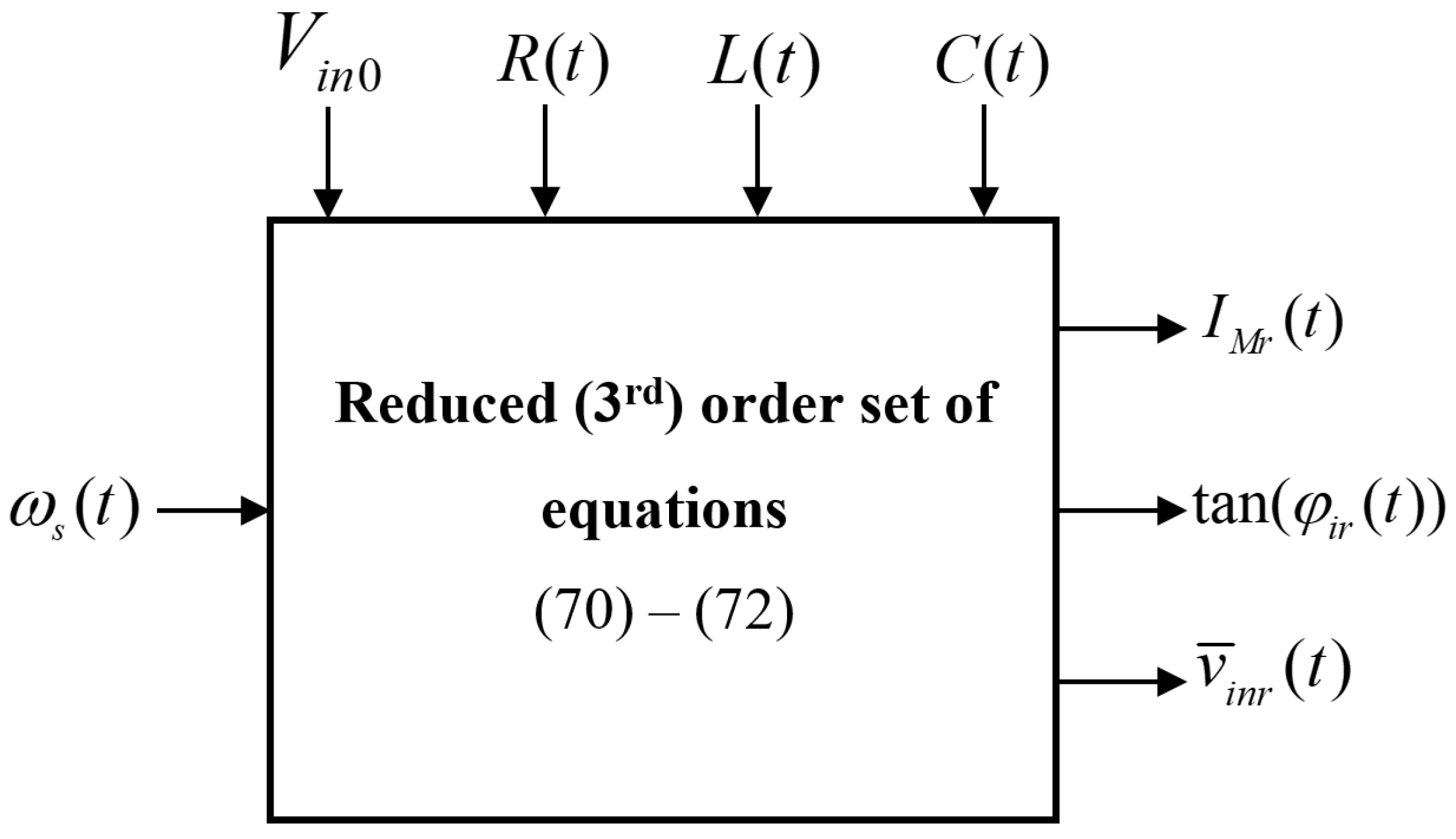
4. Envelope Model Order Reduction
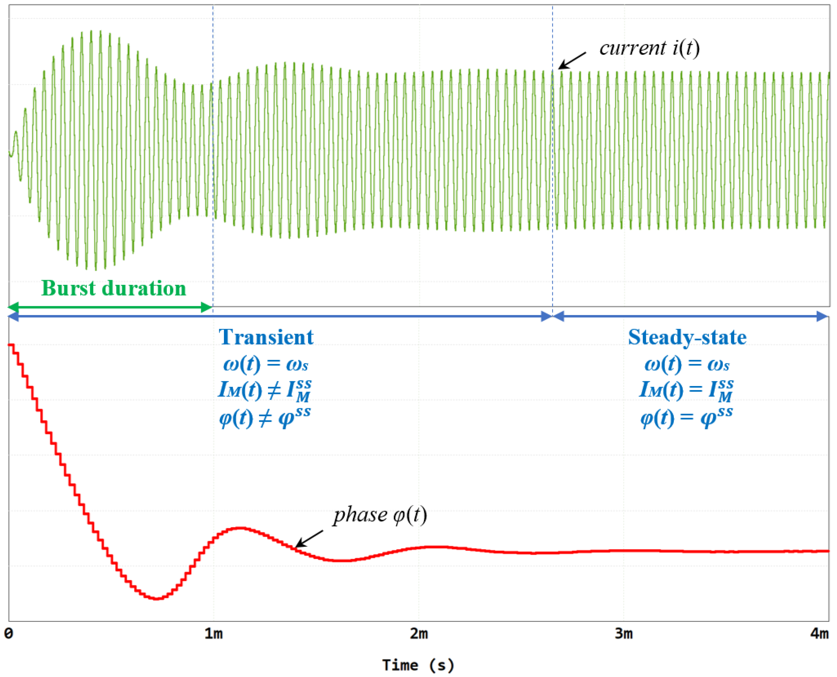
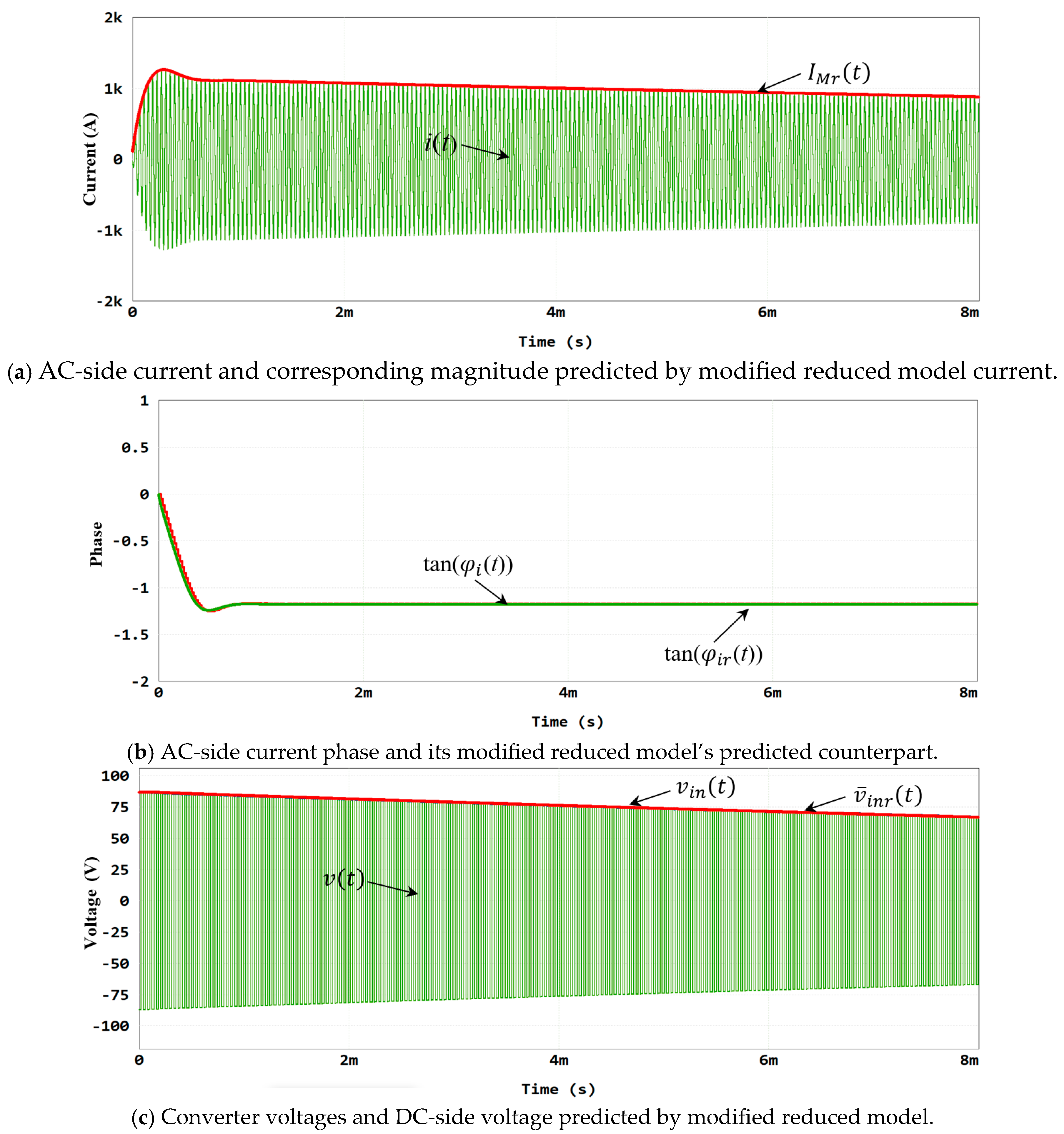
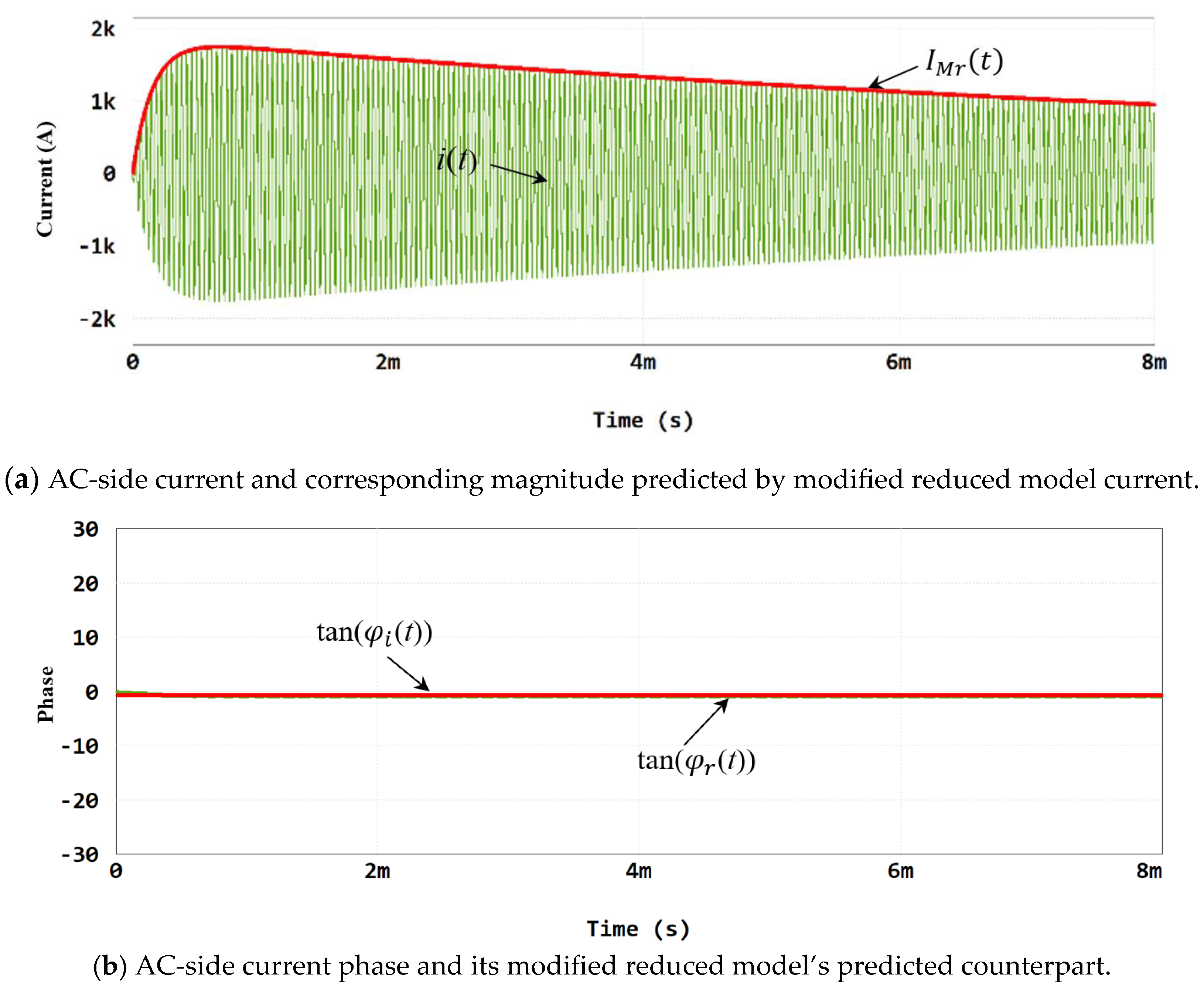
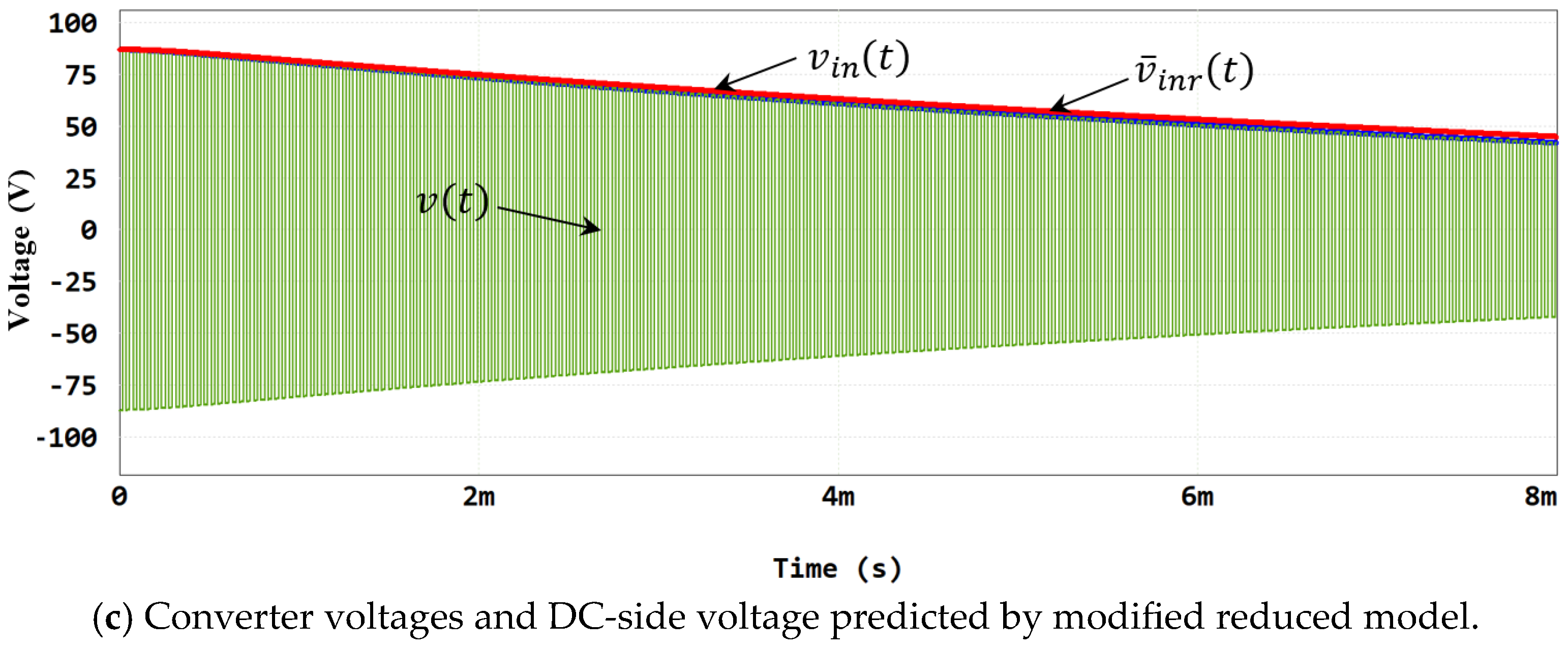
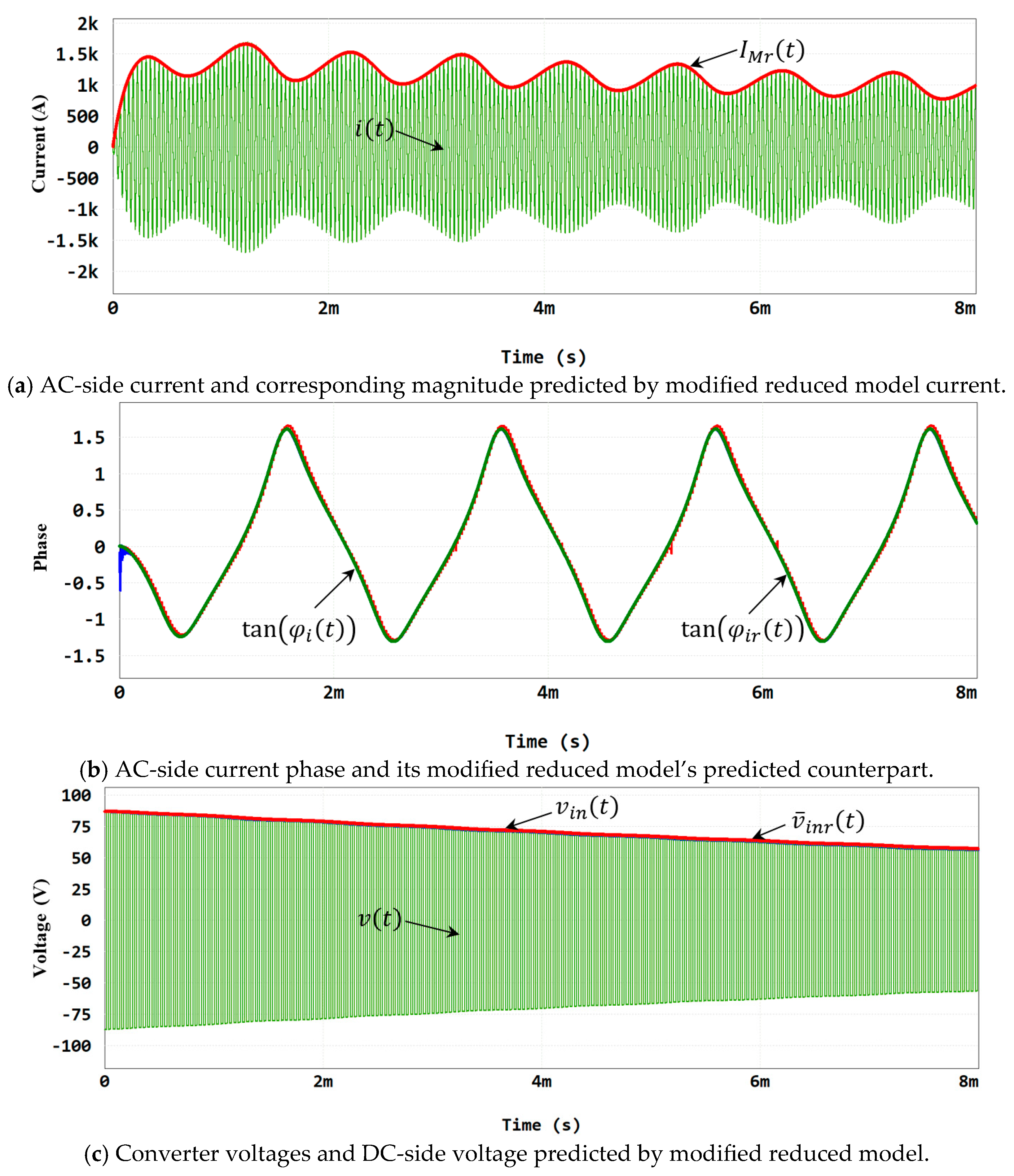
The system under consideration (cf. Figure 3) includes a single AC-side capacitor and a single AC-side inductor, indicating second-order AC-side dynamics. Considering the DC-side capacitor, third-order overall system dynamics are expected. Nonetheless, a fifth-order envelope model was derived in the preceding section. This stemmed from the nature of the sine/cosine components’ separation process adopter for the envelope dynamics capturing process, leading to system order augmentation. Therefore, original (third) model order restoration would be beneficial. The fourth-order set of equations describing the AC-side model given by (23)–(26) may be represented by the following general form:
d x ( t ) d t = A ( t ) x ( t ) + B ( t ) u ( t ) ,
where
x ( t ) = i c ( t ) i s ( t ) v C c ( t ) v C s ( t ) T ,
A ( t ) = R ( t ) + d L ( t ) d t L ( t ) ω s ( t ) 1 L ( t ) 0 ω s ( t ) R ( t ) + d L ( t ) d t L ( t ) 0 1 L ( t ) 1 C ( t ) 0 d C ( t ) d t C ( t ) ω s ( t ) 0 1 C ( t ) ω s ( t ) d C ( t ) d t C ( t ) ,
B ( t ) = 0 4 π L ( t ) 0 0 T ,     u ( t ) = v ¯ i n ( t ) .
The order of the system (38) is dictated by the size of matrix A(t). In order to reduce it, the elimination of some state equations is needed. Note that the set given in (23)–(26) may also be expressed as
d x 1 ( t ) d t d x 2 ( t ) d t = A 11 ( t ) A 12 ( t ) A 21 ( t ) A 22 ( t ) x 1 ( t ) x 2 ( t ) + B 1 ( t ) B 2 u ( t ) ,
where
x 1 ( t ) = i c ( t ) i s ( t ) T ,     x 2 ( t ) = v C c ( t ) v C s ( t ) T ,
A 11 ( t ) = R ( t ) + d L ( t ) d t L ( t ) ω s ( t ) ω s ( t ) R t + d L ( t ) d t L ( t ) ,     A 12 ( t ) = 1 L ( t ) 0 0 1 L ( t ) ,
A 21 ( t ) = 1 C ( t ) 0 0 1 C ( t ) ,     A 22 ( t ) = d C ( t ) d t C ( t ) ω s ( t ) ω s ( t ) d C ( t ) d t C ( t ) ,
B 1 ( t ) = 0 4 π L ( t ) ,     B 2 = 0 0 .
The main interest is in the DC-side-to-AC-side power transfer by means of the AC-side current, i.e., the AC-side current-related state variables x1(t) are the main interest, while the AC-side capacitor voltage-related state variables x2(t) are of secondary importance. Hence, in case a linear function F(t) satisfying
d x 2 ( t ) d t = F ( t ) d x 1 ( t ) d t
exists, substituting it into (42) would yield
x 2 ( t ) = A 22 1 ( t ) F ( t ) d x 1 ( t ) d t A 21 ( t ) x 1 ( t ) B 2 u ( t ) .
Combining (48) with (42) would eliminate the AC-side capacitor voltage-related state variables x2(t) from (42), reducing it to be a function of the state variable vector of interest x1(t) only:
d x 1 ( t ) d t = I A 12 ( t ) A 22 ( t ) F ( t ) 1 A 11 ( t ) A 12 ( t ) A 22 1 ( t ) A 21 ( t ) x 1 ( t ) + B 1 ( t ) A 12 ( t ) A 22 1 ( t ) B 2 u ( t ) .
In order to obtain the function F(t), a methodology assuming the slow-varying amplitude’s derivative and phase (SVADP) proposed in [21] is adopted hereafter. In the system under consideration, the SVADP is adopted by assumed that the capacitor voltage phase and derivative of the capacitor voltage magnitude are slow-varying functions of time. The derivative of (9) is given by
d v C ( t ) d t = d V M ( t ) d t sin θ s ( t ) + φ v ( t ) + V M ( t ) ω s ( t ) + d φ v ( t ) d t cos θ s ( t ) + φ v ( t ) ,
reducing to
d v C ( t ) d t V M ( t ) ω s ( t ) cos θ s ( t ) + φ v ( t ) ,
under the SVADP assumption. Reformulating (51) according to (13) yields
d v C ( t ) d t v C s ( t ) ω s ( t ) cos θ s ( t ) v C c ( t ) ω s ( t ) sin θ s ( t ) .
Further combining this with (5) while adopting the basic assumptions given in Section 2 yields
i ( t ) C ( t ) d v C ( t ) d t = C ( t ) ω s ( t ) v C s ( t ) cos θ s ( t ) C ( t ) ω s ( t ) v C c ( t ) sin θ s ( t ) .
Reformulating (53) according to (14) yields
v C s ( t ) cos θ s ( t ) v C c ( t ) sin θ s ( t ) = 1 C ( t ) ω s ( t ) i c ( t ) cos θ s ( t ) + i s ( t ) sin θ s ( t ) .
Separating into sine and cosine terms and equating the coefficients on both sides of each equation gives
v C s ( t ) = 1 C ( t ) ω s ( t ) i c ( t ) ,     v C c ( t ) = 1 C ( t ) ω s ( t ) i s ( t ) .
Applying the derivative to (55) results in
d v C s ( t ) d t = d C ( t ) d t ω s ( t ) + d ω s ( t ) d t C ( t ) C ( t ) ω s ( t ) 2 i c ( t ) + 1 C ( t ) ω s ( t ) d i c ( t ) d t
and
d v C c ( t ) d t = d C ( t ) d t ω s ( t ) + d ω s ( t ) d t C ( t ) C ( t ) ω s ( t ) 2 i s ( t ) 1 C ( t ) ω s ( t ) d i s ( t ) d t ,
respectively. Applying the SVADP assumption, (56) and (57) reduce to
d v C c ( t ) d t = 1 C ( t ) ω s ( t ) d i s ( t ) d t ,
    d v C s ( t ) d t = 1 C ( t ) ω s ( t ) d i c ( t ) d t .
Comparing (58) with (47), the corresponding function F(t) is obtained as
F ( t ) = 0 1 C ( t ) ω s ( t ) 1 C ( t ) ω s t 0 .
Combining (43)–(46) with (49) and (60) yields a set of two differential equations related to the AC-side current state variables:
d i c ( t ) d t = C ( t ) L ( t ) ω s 2 ( t ) ω s 2 ( t ) 1 C ( t ) L ( t ) ω s 2 ( t ) i s ( t ) + C ( t ) L ( t ) ω s 2 ( t ) R ( t ) L ( t ) i c ( t ) 1 + C ( t ) L ( t ) ω s 2 ( t ) ,
d i s ( t ) d t = C ( t ) L ( t ) ω s 2 ( t ) ω s ( t ) 1 C ( t ) L ( t ) ω s 2 ( t ) i c ( t ) C ( t ) L ( t ) ω s 2 ( t ) R ( t ) L ( t ) i s ( t ) 1 + C ( t ) L ( t ) ω s 2 ( t ) + C ( t ) L ( t ) ω s 2 ( t ) 4 v ¯ i n ( t ) π L ( t ) 1 + C ( t ) L ( t ) ω s 2 ( t ) .
The state Equations (37), (61), and (62) and the output Equations (28) and (30) form a reduced (third-order) envelope model of the system. The corresponding block diagram is depicted in Figure 5.
It should be emphasized that state variables ic(t) and is(t) neither have any physical meaning nor can be directly measured. It is, thus, proposed to perform a change of variables so that the measurable quantities (the current magnitude and phase) serve as the state variables. According to (30),
tan φ i ( t ) = i c ( t ) i s ( t ) .
The corresponding derivative is then
d d t tan φ i ( t ) = d i c ( t ) d t i s ( t ) d i s ( t ) d t i c ( t ) i s ( t ) 2 ,
Merging (63) and (64) yields
d d t tan φ i ( t ) = 1 i s ( t ) d i c ( t ) d t tan φ i ( t ) d i s ( t ) d t .
Combining (63) and (65) with (61) and (62) yields
d d t tan φ i ( t ) = C ( t ) L ( t ) ω s 2 ( t ) ω s ( t ) 1 C ( t ) L ( t ) ω s ( t ) 1 + tan 2 φ i ( t ) C t L t ω s 2 t + 1 4 v ¯ i n ( t ) π L ( t ) C ( t ) L ( t ) ω s 2 ( t ) tan φ i ( t ) i s ( t ) C ( t ) L ( t ) ω s 2 ( t ) + 1 .
The derivative of (28) is given by
d I M ( t ) d t = i s ( t ) d i s ( t ) d t + i c ( t ) d i c ( t ) d t i s ( t ) 2 + i c ( t ) 2 .
Combining (63), (65), and (67) with (61) and (62) yields
d I M ( t ) d t = C ( t ) L ( t ) ω s 2 ( t ) ω s ( t ) 1 C ( t ) L ( t ) ω s 2 ( t ) tan φ i ( t ) C ( t ) L ( t ) ω s 2 ( t ) R ( t ) L ( t ) 1 i s ( t ) C ( t ) L ( t ) ω s 2 ( t ) + 1 1 + tan 2 φ i ( t ) + + C ( t ) L ( t ) ω s 2 ( t ) 4 v ¯ i n ( t ) π L ( t ) 1 i s ( t ) 1 i s ( t ) C ( t ) L ( t ) ω s 2 ( t ) + 1 1 + tan 2 φ i ( t ) tan φ i ( t ) C ( t ) L ( t ) ω s 2 ( t ) ω s ( t ) 1 C ( t ) L ( t ) ω s 2 ( t ) + C ( t ) L ( t ) ω s 2 ( t ) R ( t ) L ( t ) tan φ i ( t ) 1 i s ( t ) C ( t ) L ( t ) ω s 2 ( t ) + 1 1 + tan 2 φ i ( t ) .
Meanwhile, the following relation holds according to (28) and (63):
i s ( t ) = I M 2 ( t ) 1 + tan 2 φ i ( t ) .
Substituting (69) into (66) and (68) and rearranging yields a modified reduced (third-order) nonlinear envelope model of the system, where subscript “r” is added to the state variables for the sake of differentiation from the full-order model counterparts:
d d t tan φ i r ( t ) = C ( t ) L ( t ) ω s 2 ( t ) ω s ( t ) 1 C ( t ) L ( t ) ω s ( t ) 1 + tan 2 φ i r ( t ) C ( t ) L ( t ) ω s 2 ( t ) + 1 1 + tan 2 φ i r ( t ) I M r 2 ( t ) · 4 v ¯ i n r ( t ) π L ( t ) C ( t ) L ( t ) ω s 2 ( t ) tan φ i r ( t ) C ( t ) L ( t ) ω s 2 ( t ) + 1 ,     tan φ i r ( 0 ) = tan φ 0
d I M r ( t ) d t = C ( t ) L ( t ) ω s 2 ( t ) ω s ( t ) 1 C ( t ) L ( t ) ω s ( t ) tan φ i r ( t ) C ( t ) L ( t ) ω s 2 ( t ) R ( t ) L ( t ) C ( t ) L ( t ) ω s 2 ( t ) + 1 1 + tan 2 φ i r ( t ) I M r ( t ) + C ( t ) L ( t ) ω s 2 ( t ) 4 v ¯ i n r ( t ) π L ( t ) 1 + tan 2 φ i r ( t ) C ( t ) L ( t ) ω s 2 ( t ) + 1 1 + tan 2 φ i r ( t ) tan φ i r ( t ) C ( t ) L ( t ) ω s 2 ( t ) ω s ( t ) 1 C ( t ) L ( t ) ω s ( t ) C ( t ) L ( t ) ω s 2 ( t ) + 1 1 + tan 2 φ i r ( t ) I M r ( t ) tan 2 φ i r ( t ) C ( t ) L ( t ) ω s 2 ( t ) R ( t ) L ( t ) C ( t ) L ( t ) ω s 2 ( t ) + 1 1 + tan 2 φ i r ( t ) I M r ( t ) ,     I M r ( 0 ) = I M 0
v ¯ i n , r ( t ) C i n d v ¯ i n , r ( t ) d t = R t I M r ( t ) 2 2 ,   v ¯ i n r ( 0 ) = V i n 0
with matching general initial conditions. The resulting block diagram is shown in Figure 6.

5. Verification

In order to validate the derived modified reduced envelope model, the circuit shown in Figure 3 was simulated using the PSIM 2025 software concurrently using the component-level circuit and the equations of the modified reduced envelope model. The corresponding values of the system parameters are summarized in Table 2. The simulations were carried out with the RLC network parameters, varying in time according to (cf. (1)):
Δ R ( t ) = R 1 sin 2 π f 1 t , Δ L ( t ) = L 1 sin 2 π f 1 t , Δ C ( t ) = C 1 sin 2 π f 1 t   .
The nominal resonant frequency of the system is defined as
f 0 = 1 2 π C 0 L 0 = 25.3 [ kHz ] .
Six simulations were carried out (referred to as Sim 1–Sim 6 in Table 3, summarizing the corresponding parameter variations), with φv taken as the reference phase and the φi of the switched device-level model obtained using the method proposed in [33].
In the first three simulations, the parameter values of the RLC network components remained nominal and constant. The system behavior was then captured for an operational frequency above resonance (Sim 1, Figure 7; φi < 0), below resonance (Sim 2, Figure 8; φi > 0), and at resonance (Sim 3, Figure 9; φi = 0). For clarity, the zoomed waveforms of the DC-side converter input voltage, AC-side output converter voltage, and AC-side current at, above, and below resonance are depicted in Figure 10. In the next three simulations, the responses of the system operating at the resonant frequency to variations in the inductance only (Sim 4, Figure 11), inductance and capacitance (Sim 5, Figure 12), and all three parameters (Sim 5, Figure 13) were obtained. It is well-evident that the modified nonlinear reduced-order model output accurately followed the envelope behavior of the switched component-level circuit in all examined cases. Consequently, the proposed model may be adopted for establishing a feedback controller aiming to regulate the AC-side magnitude and/or phase.

6. Conclusions

This paper suggested a process of reduced-order nonlinear dynamic envelope modeling applied to a capacitor-powered resonant inverter feeding a time-varying series RLC load, often employed in pulsed-power applications. Such arrangements are particularly challenging due to the fact that their operation time is lower than the corresponding system settling time, imposing significant large-signal operation point variations, thus making classical linearization-based reduced models invalid. The derived third-order model (attained by applying an SVADP assumption, which also imposes the proposed methodology limitation) was proven to accurately represent the highly nonlinear time-varying behavior of the fifth-order model during transients, where conventional simplified models fall short. Future work on this subject will focus on a feedback controller design based on the derived nonlinear model of the system and the investigation of a possible negative interaction between the controller and the plant (see, e.g., [34]). In addition, a high-current resonant inverter prototype is currently being developed, so a feedback control algorithm designed according to the proposed methodology is expected to be validated experimentally in the near future.

Author Contributions

Conceptualization, O.A. and A.K.; methodology, A.K.; software, O.A.; validation, O.A.; formal analysis, O.A.; investigation, O.A.; resources, A.K.; data curation, O.A.; writing—original draft preparation, O.A.; writing—review and editing, A.K.; visualization, O.A.; supervision, A.K.; project administration, A.K.; funding acquisition, A.K. All authors have read and agreed to the published version of the manuscript.

Funding

This research received no external funding.

Data Availability Statement

The original contributions presented in this study are included in the article. Further inquiries can be directed to the corresponding author.

Conflicts of Interest

The authors declare no conflicts of interest.

References

  1. Garcia-Michelena, P.; Ruiz-Reina, E.; Herrero-Dorca, N.; Chamorro, X. Multiphysics modeling and experimental validation of heat and mass transfer for the vacuum induction melting process. Appl. Therm. Eng. 2024, 243, 122562. [Google Scholar] [CrossRef]
  2. Vishnuram, P.; Ramachandiran, G.; Sudhakar Babu, T.; Nastasi, B. Induction heating in domestic cooking and industrial melting applications: A systematic review on modelling, converter topologies and control schemes. Energies 2021, 14, 6634. [Google Scholar] [CrossRef]
  3. Lee, S.-Y.; Gho, J.-S.; Kang, B.-H.; Cho, J.-S. Analysis of Pulse Power Converter for Plasma Application. In Proceedings of the 34th Annual Conference of IEEE Industrial Electronics Society, Orlando, FL, USA, 10–13 November 2008. [Google Scholar]
  4. Cho, D.; Suh, N.P.; Yoon, U.; Jung, G. Shaped Magnetic Field in Resonance Technology and Its Application to Transportation System. In Proceedings of the International ASME Mechanical Engineering Congress and Exposition, Houston, TX, USA, 13–19 November 2015. [Google Scholar]
  5. Baimel, D.; Kuperman, A. Multi-regional modeling and operational analysis of LC/S-compensated inductive wireless power transfer link with load-independent current output. Simul. Model. Pract. Theory 2020, 105, 102154. [Google Scholar] [CrossRef]
  6. Vulfovich, A.; Baimel, D.; Kuperman, A. Modified first harmonic approximation-based modeling of SN-compensated inductive power transfer links operating at load-independent-voltage-output frequency. Simul. Model. Pract. Theory 2021, 111, 102340. [Google Scholar] [CrossRef]
  7. Hui, S.Y. Planar wireless charging technology for portable electronic products and Qi. Proc. IEEE 2013, 101, 1290–1301. [Google Scholar] [CrossRef]
  8. Si, P.; Hu, A.P.; Malpas, S.; Budgett, D. A frequency control method for regulating wireless power to implantable devices. IEEE Trans. Biomed. Circuits Syst. 2008, 2, 22–29. [Google Scholar] [CrossRef] [PubMed]
  9. Baek, S. Trajectory control approach for single-stage soft-switching grid-tied inverters. Appl. Sci. 2024, 14, 10940. [Google Scholar] [CrossRef]
  10. Aksöz, A. Creating a quasi-resonant induction cooktop integrating zero-voltage switching (ZVS) and load management. Appl. Sci. 2024, 14, 10449. [Google Scholar] [CrossRef]
  11. Sassonker, I.; Shvartsas, M.; Shoihet, A.; Kuperman, A. Modeling of Electromagnetic Levitation Melting System with Experimental Validation. In Proceedings of the IEEE International Conference on the Science of Electrical Engineering in Israel, Eilat, Israel, 12–14 December 2018. [Google Scholar]
  12. Sassonker, I.; Kuperman, A. Electro-mechanical modeling of electromagnetic levitation melting system driven by a series resonant inverter with experimental validation. Energy Convers. Manag. 2020, 208, 112578. [Google Scholar] [CrossRef]
  13. Jang, E.; Kwon, M.J.; Park, S.M.; Ahn, H.M.; Lee, B.K. Analysis and design of flexible-surface induction-heating cooktop with GaN-HEMT-based multiple inverter system. IEEE Trans. Power Electron. 2022, 37, 12865–12876. [Google Scholar] [CrossRef]
  14. Vulfovich, A.; Kolesnik, S.; Baimel, D.; Cohen, E.; Gutman, M.; Geftler, A.; Kuperman, A. Output characteristics of none-series compensated inductive wireless power transfer link operating at load-independent-voltage-output frequency. Simul. Model. Pract. Theory 2021, 115, 102424. [Google Scholar] [CrossRef]
  15. Gupta, A.; Yadav, O.P.; DeVoto, D.; Major, J. A Review of Degradation Behavior and Modeling of Capacitors. In Proceedings of the International Technical Conference and Exhibition on Packaging, San Francisco, CA, USA, 27–30 August 2018. [Google Scholar]
  16. Ji, C.; Zanchetta, P.; Carastro, F.; Clare, J. Repetitive control for high-performance resonant pulsed power supply in radio frequency applications. IEEE Trans. Ind. Appl. 2014, 50, 2660–2670. [Google Scholar] [CrossRef]
  17. Almer, S.; Jonsson, U. Dynamic phasor analysis of periodic systems. IEEE Trans. Autom. Control 2009, 54, 2007–2012. [Google Scholar] [CrossRef]
  18. Sassonker, I.; Elkayam, M.; Kuperman, A. Modeling Technique of Large Signal Dynamics for Electromagnetic Levitation Melting System. In Proceedings of the IEEE East-West Design & Test Symposium, Batumi, Georgia, 13–16 September 2019. [Google Scholar]
  19. Sassonker, I.; Kuperman, A. Envelope dynamics of resonant inverter driven electromagnetic levitation melting system with experimental verification. Mech. Syst. Signal Process. 2020, 140, 106704. [Google Scholar] [CrossRef]
  20. Sassonker, I.; Sassonker (Elkayam), M.; Shvartsas, M.; Darhovsky, Y.; Shoihet, A.; Kuperman, A. Small-signal modeling and active damping of resonant electromagnetic levitation melting system with experimental verification. Energy Convers. Manag. 2020, 215, 112906. [Google Scholar] [CrossRef]
  21. Dominguez, A.; Barragan, L.A.; Artigas, J.I.; Otin, A.; Urriza, I.; Navarro, D. Reduced-order models of series resonant inverters in induction heating applications. IEEE Trans. Power Electron. 2017, 32, 2300–2311. [Google Scholar] [CrossRef]
  22. Li, H.; Wang, K.; Huang, L.; Chen, W.; Yang, X. Dynamic modeling based on coupled modes for wireless power transfer systems. IEEE Trans. Power Electron. 2015, 30, 6245–6253. [Google Scholar] [CrossRef]
  23. Wang, W.; Song, Q.; Zhang, S.; Li, Y.; Ahmad, M.; Gong, Y. The loss analysis and efficiency optimization of power inverter based on sic mosfets under the high-switching frequency. IEEE Trans. Ind. Appl. 2021, 57, 1521–1534. [Google Scholar] [CrossRef]
  24. Ge, X.; Wang, Y.; Ren, D.; Tang, M.; Wang, L. A single-input multi-output inverter with voltage boosting for multi-load wireless power transfer systems. Appl. Sci. 2024, 14, 10453. [Google Scholar] [CrossRef]
  25. Almutairi, S.Z. Dynamic interactions between parallel grid-forming inverters in a microgrid. Appl. Sci. 2023, 13, 6989. [Google Scholar] [CrossRef]
  26. Elkayam, M.; Frechter, Y.; Sassonker, I.; Kuperman, A. Virtual Impedance Control for Efficient Power Transfer in Electromagnetic Levitation Melting System. In Proceedings of the IEEE Wireless Power Week Conference, London, UK, 18–21 June 2019. [Google Scholar]
  27. Yin, Y.; Zane, R.; Erickson, R.; Glaser, J. Direct Modeling of Envelope Dynamics in Resonant Inverters. In Proceedings of the 34th IEEE Power Electronics Specialists Conference, Acapulco, Mexico, 15–19 June 2003. [Google Scholar]
  28. Oliver, J.; Fernandez, C.; Prieto, R.; Cobos, J. Circuit Oriented Model of Rectifiers for Large Signal Envelope Simulation. In Proceedings of the 36th IEEE Power Electronics Specialists Conference, Dresden, Germany, 16 June 2005. [Google Scholar]
  29. Lineykin, S.; Ben-Yaakov, S. Unified SPICE compatible model for large and small-signal envelope simulation on linear circuits excited by modulated signals. IEEE Trans. Ind. Electron. 2006, 53, 745–751. [Google Scholar] [CrossRef]
  30. Bertoluzzo, M.; Giacomuzzi, S.; Forato, M. Performance analysis of envelope modelling applied to resonant converters. IEEE Trans. Ind. Electron. 2022, 69, 4046–4055. [Google Scholar] [CrossRef]
  31. Tian, S.; Lee, F.C.; Li, Q. A simplified equivalent circuit model of series resonant converter. IEEE Trans. Power Electron. 2016, 31, 3922–3931. [Google Scholar] [CrossRef]
  32. Akler, O.; Siton, Y.; Kuperman, A. Envelope Modeling of Capacitor-Powered Resonant Inverter Feeding a Time-Varying Series RLC Load. In Proceedings of the 18th IEEE International Conference on Compatibility, Power Electronics and Power Engineering, Gdynia, Poland, 24–26 June 2024. [Google Scholar]
  33. Johansson, L.A.; Ramaswamy, A.; Vikash; Rodwell, M. Coherent Optical Receiver with Linear XOR Phase Detection and Frequency Down-Conversion. In Proceedings of the IEEE MTT-S International Microwave Symposium Digest, Boston, MA, USA, 7–12 June 2009. [Google Scholar]
  34. Haro-Larrode, M.; Eguia, P.; Santos-Mugica, M. Analysis of voltage dynamics within current control time-scale in a VSC connected to a weak AC grid via series compensated AC line. Electr. Power Syst. Res. 2024, 229, 110189. [Google Scholar] [CrossRef]
Figure 1. Series capacitor addition to RL load to allow resonant operation.
Applsci 15 04502 g001
Figure 2. RLC network current response to sinusoidal voltage excitation at t = 0.
Applsci 15 04502 g002
Figure 3. System under consideration.
Applsci 15 04502 g003
Figure 4. Full-order envelope model of the system.
Applsci 15 04502 g004
Figure 5. Reduced-order envelope model of the system.
Applsci 15 04502 g005
Figure 6. Modified reduced-order envelope model of the system.
Applsci 15 04502 g006
Figure 7. Results of Simulation 1.
Applsci 15 04502 g007
Figure 8. Results of Simulation 2.
Applsci 15 04502 g008
Figure 9. Results of Simulation 3.
Applsci 15 04502 g009aApplsci 15 04502 g009b
Figure 10. Zoomed-in steady-state converter’s voltages and AC-side current.
Applsci 15 04502 g010
Figure 11. Results of Simulation 4.
Applsci 15 04502 g011
Figure 12. Results of Simulation 5.
Applsci 15 04502 g012
Figure 13. Results of Simulation 6.
Applsci 15 04502 g013
Table 1. Modeling methods comparison.
MethodValid in Steady StateValid in Transients
Classical phasor-domain analysis [17]YesNo
Linearized reduced-order envelope modeling [21]YesSmall variations only
Energetic coupling envelope modeling [22]NoNear resonance only
Proposed nonlinear reduced-order envelope modelNoYes
Table 2. System parameter values.
ParameterValueUnit
V087V
Cin80mF
f1500Hz
IM00A
tan(φ0)0----
R061mΩ
L04.6μH
C08.58μF
Table 3. Varying parameter values.
ParameterSimulation Parameters
Sim 1Sim 2Sim 3Sim 4Sim 5Sim 6
fs [Hz]1.05f00.95f0f0f0f0f0
L1 [H]0000.05L00.05L00.05L0
C1 [F]00000.05C00.05C0
R1 [Ω]000000.05R0
Disclaimer/Publisher’s Note: The statements, opinions and data contained in all publications are solely those of the individual author(s) and contributor(s) and not of MDPI and/or the editor(s). MDPI and/or the editor(s) disclaim responsibility for any injury to people or property resulting from any ideas, methods, instructions or products referred to in the content.

