2. FSMs and FPGAs: Background Information
An FSM can be defined as a six-tuple
[
29], where
is a set of internal states,
is a set of inputs,
is a set of outputs,
is a transition function,
is a function of the output, and
is an initial state. An FSM can be represented using various tools, such as state transition graphs (STGs) [
4], state transition tables (STTs) [
29], algorithmic state machines [
30], binary decision diagrams [
10,
31], and-inverter graphs [
32], and graph-schemes of algorithms [
29]. In this survey, we used either STGs or STT for the specification of FSMs.
The FSM states are represented by the nodes of an STG. The arcs connecting the nodes define the interstate transitions determined by the input signals which are the conjunctions of inputs
(or their complements). These conjunctions are written above the arcs together with the outputs generated during the transitions. To design an FSM circuit, an STG should be transformed into the corresponding STT. An STT includes the following columns [
29]:
is a current state;
is a state of transition;
is an input signal determining a transition from
to
;
is a subset of the set
Y generated during the particular transition. We name this subset a collection of outputs. The numbers of transitions (
are shown in the last column of the STT.
There are two main types of FSM, namely, Mealy [
33] and Moore FSMs [
34]. The first of them was proposed in 1955 by G. Mealy; the second was proposed in 1956 by E. Moore. In both cases, the function
determines the states of transition as functions depending on the current states and inputs. Thus, it is the following function:
For Mealy FSMs, the function
determines the outputs as functions depending on the current states and inputs. It gives the following function:
For Moore FSMs, the function
determines the outputs with the following function:
In this article, we mostly analyze the reduced power consumption (RPC) methods for Mealy FSMs. Our choice is explained by the fact that these methods are widely represented in the open scientific and technical literature.
In 1965, Viktor Glushkov proved a theorem on the structural completeness of FSMs [
35]. According to this theorem, an FSM circuit is represented as a composition of the combinational part and the memory. The memory is necessary to keep the history of the FSM operation. The history is represented by FSM internal states. This fundamental approach is still widely used for the synthesis of FSM circuits.
An FSM logic circuit is represented by some systems of Boolean functions (SBFs) [
29]. To find these SBFs for Mealy FSMs, it is necessary to [
29]: (1) encode states
by binary codes
; (2) construct sets of state variables
and input memory functions (IMFs)
; and (3) transform an initial STT into a direct structure table (DST). States
are encoded during the step of state assignment [
4].
The minimum possible number of state variables
RS is determined by
The approach based on (
4) defines so-called maximum binary codes [
4]. This method is used, for example, in the well-known academic system SIS [
36]. But the number of state variables can be different from (
4). For example, the one-hot state codes with
are used in the academic system ABC [
32,
37] of Berkeley. The maximum binary codes and one-hot codes define extreme points of the encoding space. There are other approaches for state assignment where the following relation holds:
.
A state register (RG) keeps the state codes. The register includes
R memory elements (flip-flops) having shared inputs of synchronization (
Clock) and reset (
Start). Very often, master–slave D flip-flops are used to organize state registers [
38,
39]. The pulse
Clock allows the functions
to change the RG content.
After the execution of the state assignment, we should create a direct structure table. A DST includes all columns of an STT and three additional columns. These columns include the current state codes
and the codes
of the states of transitions. At last, a column
includes the symbols
corresponding to ones in the code
from the row
of a DST
). A DST is a base to construct the following SBFs:
SBF (
5) corresponds to function (
1), SBF (
6) to function (
2). Systems (
5)–(
6) determine a structural diagram of a so-called P Mealy FSM (
Figure 1) [
39].
The combinational part consists of two blocks. The block of input memory functions generates functions (
5). The block of outputs generates system (
6). The pulse
Start writes the code of the initial state to RG. The pulse of the synchronization
Clock allows information to be written to the register.
In this survey, we mostly discuss the RPC methods for FPGA-based Mealy FSMs. Let us shortly describe the peculiarities of FPGAs.
As a rule, modern FPGAs have an “island-style” architecture [
40]. They include different configurable logic blocks (CLBs) and a matrix of programmable interconnections [
23,
24,
25]. To implement an FSM circuit, we can use either CLBs consisting of look-up table (LUT) elements or embedded memory blocks (EMBs). The output of a LUT can be connected with a flip-flop through a dedicated multiplexor. The flip-flops are necessary for implementing register circuits of sequential blocks [
6]. This register is distributed among the LUTs implementing IMFs. The EMBs are synchronous blocks; thus, there is no need for an additional register to keep FSM state codes.
A LUT consists of SRAM cells and can keep a truth table of an arbitrary Boolean function having up to S
L arguments [
40,
41]. The main feature of a LUT is an extremely small number of inputs, S
L. In modern FPGAs, the number of LUT inputs does not exceed six [
23,
24,
25]. If some Boolean function depends on more than S
L arguments, it should be transformed using some methods of functional decomposition [
41]. It results in multi-level FSM circuits with irregular systems of interconnections. Such circuits resemble programs based on an intensive use of “go-to” operators [
42]. Using terminology from programming, we can say that the functional decomposition produces LUT-based circuits with “spaghetti-type” interconnections.
A chip area occupied by a LUT-based FSM circuit is determined mostly by the number of LUTs and the system of their interconnections. Obviously, to reduce the occupied area, it is necessary to reduce the number of LUTs in a circuit. The number of LUTs also influences the power consumption. As noted in [
43], “process technology has scaled considerably... with current design activity at 14 and 7 nm”. Hence, interconnection delay now dominates logic delay [
43]. Also, it is known that interconnections are responsible for consuming up to 70% of the energy [
40,
44]. Thus, to reduce the consumed energy, it is necessary to reduce the number of interconnections. This improves both the operating frequency and power consumption.
Modern FPGAs include a lot of configurable embedded memory blocks [
25]. The EMBs allow the implementation of systems of regular functions [
45]. The replacement of LUTs by EMBs allows one to significantly improve the characteristics of resulting FSM circuits [
46]. Because of it, there are a lot of design methods targeting EMB-based FSMs [
22,
46,
47,
48,
49,
50,
51,
52,
53,
54,
55,
56]. The survey of different methods of EMB-based design can be found in [
45]. Unfortunately, these methods can be used only if there are “free” EMBs, which are not used to implement other parts of a digital system.
An EMB can be characterized by a pair
, where
is a number of address inputs, and
is a number of memory cell outputs. A single EMB can keep a truth table of an SBF including up to
Boolean functions depended on up to
arguments [
57]. A pair
defines a configuration of an EMB with a constant total number of bits (size of EMB):
The parameters
and
could be defined by a designer [
58]. It means that EMBs are configurable memory blocks [
59]. The following configurations exist for modern EMBs [
25]:
, …,
. Therefore, modern EMBs are very flexible and can be tuned to meet the characteristics of a particular FSM. Because of it, there are a lot of design methods for EMB-based FSMs [
22,
46,
47,
48,
49,
50,
51,
52,
53,
54,
55,
56].
If the condition
holds, then an FSM circuit is implemented as a single EMB [
45]. If (
8) is violated, then an FSM circuit could be implemented as (1) a network of EMBs or (2) a network of LUTs and EMBs [
46,
55].
3. Methods of Reducing Power Consumption in CMOS Integrated Circuits
The CMOS technology uses metal–oxide–semiconductor (MOS) field-effect transistors to create gates, flip-plops, and memory blocks such as RAM and ROM, and so on [
60]. Each gate uses complementary and symmetrical pairs of p-type and n-type transistors. For example, it requires two MOS transistors to implement the circuit of a NOT gate (
Figure 2a).
The NOT gate operates in the following manner. If the voltage
“0”, then the equivalent electrical circuit is shown in
Figure 2b. The transistor T
A is open; its resistance
. At the same time, the transistor T
B is closed, and its resistance R
B is close to infinity. It means that the following relation takes place:
“1”. If
“1”, then T
A is closed (its resistance is close to infinity) and T
B is open (its resistance is close to zero). It gives
(
Figure 2c). This situation is common: if one of transistors is open, then the second transistor of the pair is closed.
Of course, there is an ideal mode of operation shown in
Figure 2. In this ideal case, there is no current between
and
GND. Thus, the so-called leakage current
is absent. But in reality, the resistance of a closed transistor is far from infinity, and the resistance of an open transistor is greater than zero. This means that a small leakage current still exists. This current is responsible for the static power consumption of a CMOS gate in its stable state.
There is parasitic load capacitance between the wires and . It is responsible for a dynamic power consumption of a gate. Obviously, it takes some time to charge (from “0” to “1”) or discharge (from “1” to “0”) the parasitic capacitor . Until the final stable voltage (either “0” or “1”) is established at the gate output, some power is consumed.
When a gate is switched, there is a very small instant of time when both transistors are open. It means that during that time, there is a short circuit current between the voltage source and the ground, .
Therefore, there are two categories of power consumption in CMOS gates: static and dynamic. The static power
is connected with the existence of the leakage current
. The static power is determined as follows [
61,
62]:
The dynamic power
is connected mostly with the charging and discharging of the capacitor
. It is determined by the following expression [
63]:
In (
10), the symbol
stands for a switching activity,
is an operating frequency.
Up to this point, we have analyzed 64 articles and monographs. Summarizing the analysis of these sources, we can list some reasons showing the importance of reducing power consumption. They are the following:
All these factors should be taken into account in the process of FPGA-based FSMs’ design. To achieve this, it is necessary to have efficient methods for reducing the power consumption represented by (
9)–(
10). How can it be done?
As follows from (
9), the static power is determined by technology. It is shown in [
66] that the value of
increases drastically with CMOS scaling. The higher the FPGA chip density is, the higher the value of
is. Obviously, within a certain technology, the static power consumption of VLSI-based FSM circuit could be decreased by reducing the chip area occupied by an FSM circuit. Thus, it is necessary to reduce the quantity of internal occupied resources (IORs) used by an FSM circuit. It means that it is necessary to improve methods of IOR optimization used in VLSI-based FSM design.
The analysis of (
10) shows that the value of
can be reduced by reducing the value of
. This can be achieved simply by improving the semiconductor technology. Next, the reducing supply voltage
significantly diminishes the value of
, but it diminishes the possible operating frequency of an FSM circuit. Reducing the value of
also leads to a decrease in
. But very often, there is a deadline for producing FSM outputs
. For example, it is very important for real-time embedded systems [
14,
67,
68]. An FSM is a part of some digital system including various operational blocks. The lower the operating frequency, the more time is required by a system to fulfill a specific task. The system’s consumed energy depends on the time of system operation. It means that reducing the
of an FSM can increase the overall power consumption of a digital system.
To control the values of
and
, various methods of dynamic voltage and frequency scaling (DVFS) can be used [
3]. Also, it can be done using low-power modes. These methods belong to a group of power mode management (PMM) sometimes named dynamic power management (DPM) [
69].
Thus, only a parameter whose value can be changed due to the synthesis strategy represents a switching activity. To minimize the value of
, various methods of state assignment can be used [
70]. We discuss them a bit later.
The analysis of the literature allows us to classify the known RPC methods. This classification is shown in
Figure 3.
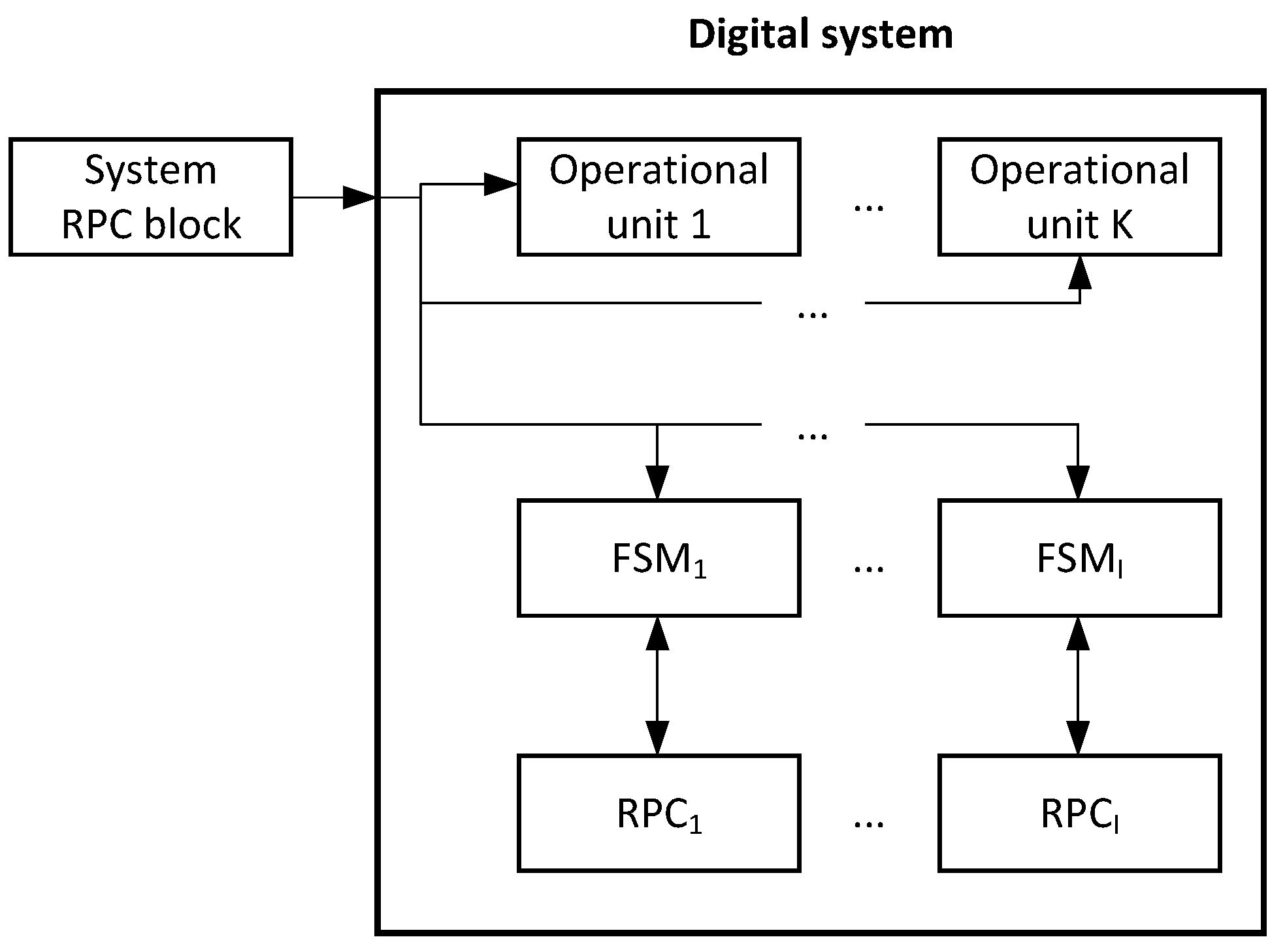
We have divided RPC methods into two groups. The coarse-grained methods (CGMs) are the same for any block of a digital system. The fine-grained methods (FGMs) take into account specifics of a particular block. As a rule, all these methods assume the presence of some additional block providing the RPC (
Figure 4).
The system’s RPC block executes rules of DVFS accepted in a particular digital system. It could be either the voltage scaling or clock frequency scaling or both. For example, the value of can be reduced for any operational or sequential block such as FSM. Also, either or Clock could be cut off a particular block. The system’s RPC can replace the voltage by some other voltage to reduce the values of leakage currents.
Obviously, if either
or
, then
. This follows from (
10). From (
9), diminishing the value of
leads to reducing the value of
. This is a positive effect of DVFS. But this approach also has two negative effects [
69]. Firstly, to implement the system’s RPC block, it is necessary to use some IORs. Thus, this block requires an additional chip area. Also, the block consumes some power and adds to the system’s latency time. If
, then an FSM is in the idle mode (it is “sleeping”). To “wake up” an FSM, it is necessary to start the clock generator. In turn, the generator takes some time to stabilize the operating frequency. An increase in the latency time is the second negative effect of DVFS.
Therefore, DVFS is connected with a so-called power overhead [
70]. The power overhead includes the three following components: the extra chip area, additional power consumption, and increased latency time. It is necessary to find a reasonable trade-off between the inevitable overhead and the required characteristics of a digital system. We do not discuss these methods in this paper.
As follows from
Figure 3, there are three groups of fine-grained methods of RPC. The clock-gating (CG) approach is connected with interrupting connections between the clock generator and synchronization inputs of flip-flops. There are two approaches based on CG: (1) the decomposition of an FSM and (2) the input disability. This approach is connected with using additional blocks
to control the timing of automata
(
Figure 4). Thus, this approach is connected with an RPC overhead.
The second group of FGMs consists of special methods of state assignment. The states
are encoded in a way that reduces the value of switching activity
. From (
10), this reduces the value of
(if
,
, and
have constant values). Sometimes, this leads to increasing the value of the bit depth of state codes,
R, compared to its minimum value determined by (
4). This growth is the RPC overhead for this group of FGM.
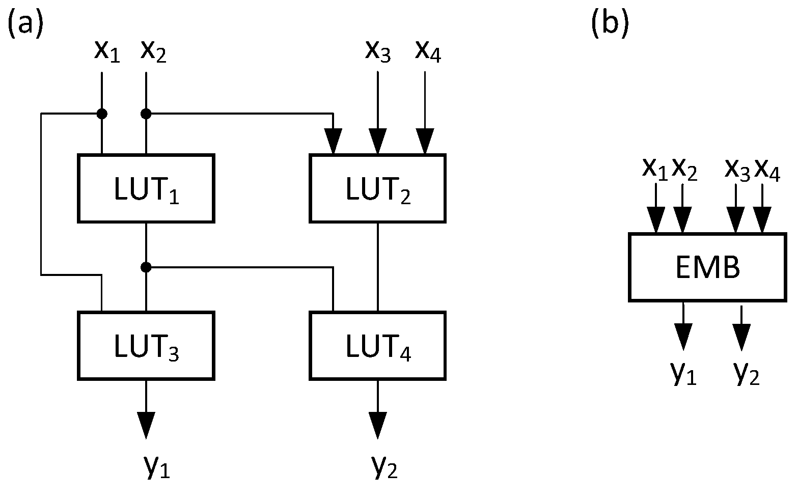
The third group is based on the replacement of LUTs by EMBs. In fact, we are moving from fine-grained LUTs to coarse-grained EMBs. As follows from
Figure 5, some group consisting of four LUTs and their interconnections is replaced by a single EMB.
The circuit (
Figure 5a) consists of 4 LUTs and 11 interconnections. It is replaced by the circuit having a single EMB and six interconnections (
Figure 5b). These interconnections correspond to inputs and outputs of this circuit. There are no additional interconnections which can be found in the LUT-based circuit (
Figure 5a). Obviously, the EMB-based circuit has better area, time, and power characteristics than the equivalent LUT-based circuit. It does not require any power overhead. But this approach has two limitations. First, it can be used if there are “free” EMBs (very often, EMBs are used for implementing operational blocks of a system). Second, an EMB can be used if the number of arguments of an SBF does not exceed the number of address inputs,
.
Now, we discuss the most known fine-grained methods of reducing power consumption in the next three Sections of this survey. These methods are the clock-gating, FSM decomposition, state assignment restricting the switching activity, and replacing LUTs by EMBs.
4. Saving Power by Clock-Gating and FSM Decomposition
In Mealy FSMs, outputs
are unstable [
39]. Because outputs
depend on inputs
, then changing inputs during the clock cycle may cause short-term changes in outputs (glitches). This may cause a malfunction of a digital system. To stabilize the outputs, it is sufficient to stabilize the FSM inputs. This can be achieved by entering a special register
as shown in
Figure 6. This figure also depicts the interaction of an FSM with other digital system blocks.
To generate correct output values, an FSM should analyze the outputs of other blocks. They form the set
. When values of the inputs are correct, the pulse
Clock1 is generated. The values of FSM inputs are loaded into
RGX. Now, they correspond to registered inputs from a set
. The elements of
are stable during the cycle of
Clock. Thus, an FSM generates the following SBF:
Now, the outputs are stable after the completion of various transients in the FSM circuit.
Let us point out that there is no need of RGX if the model of a Moore FSM is used. This is connected with the nature of outputs (
3). From (
3), there is no direct dependence between the inputs and outputs of a Moore FSM. The outputs depend only on states. Thus, the outputs are registered. The state register outputs (state variables) are stable during each cycle of operation. Therefore, if some input is changed between two pulses of synchronization, the outputs are unchangeable.
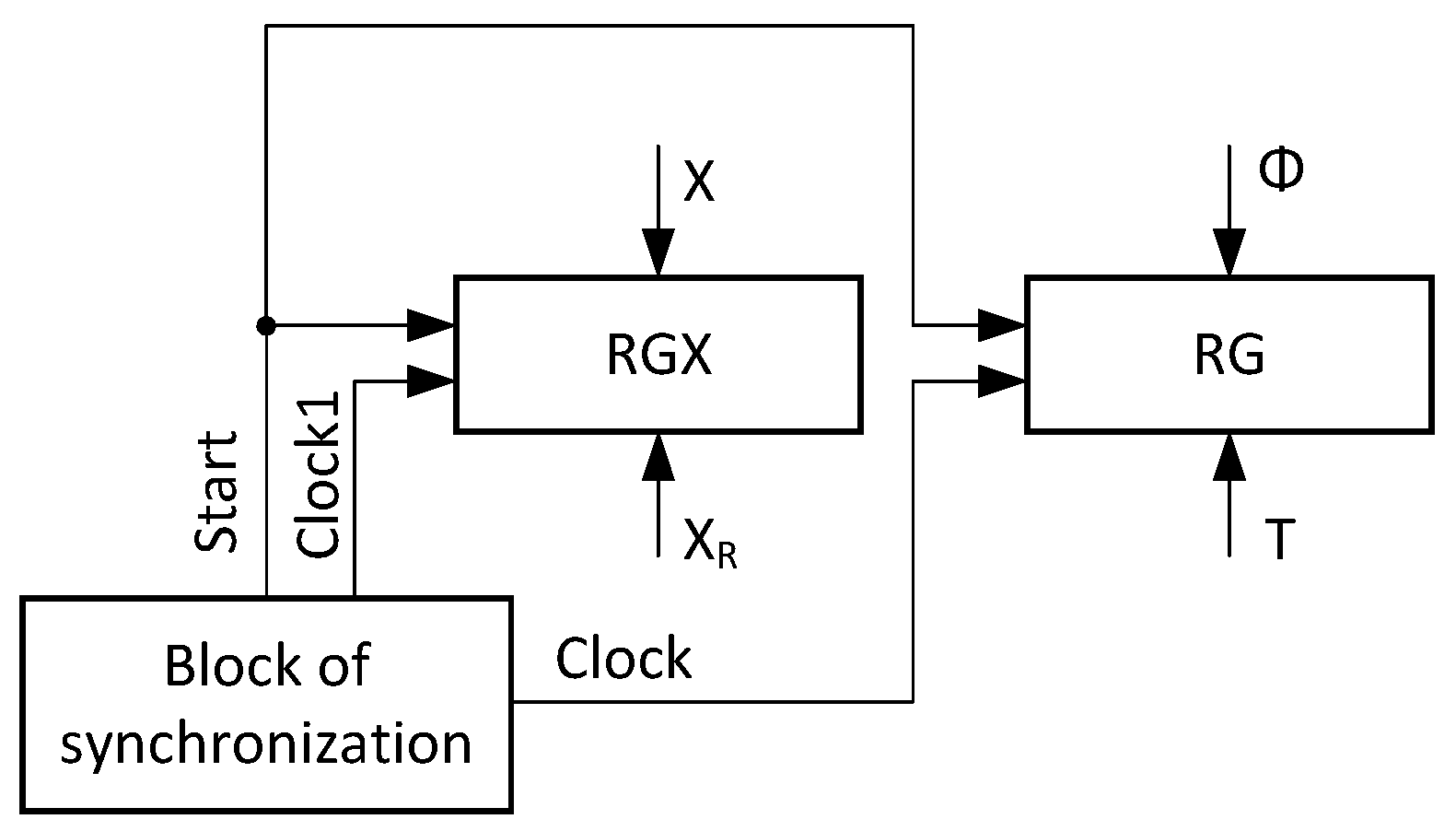
Thus, in reality, there are two registers in the circuits of Mealy FSMs. The register
includes
R flip-flops, the register
consists of
L flip-flops. These registers are synchronized by different pulses (
Figure 7).
The pulses
Clock1 and
are generated by the special block of synchronization. This block contains a quartz generator, delay circuit, and a single vibrator generating the pulse
Start. It is known that clock trees usually consumes up to 50% of the dynamic power [
71]. The internal switching power of flip-flops is responsible for 45–50% of the clock tree’s power consumption [
72]. As a result, it is very important to deliver synchronization pulses only to flip-flops whose states will be changed in a particular cycle of FSM operation. This can be achieved by using the clock-gating approach.
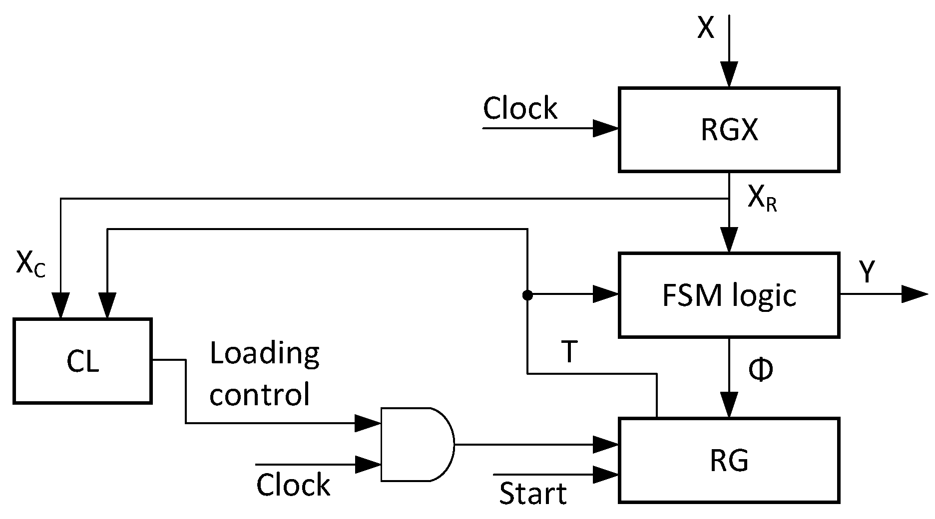
CG assumes using an additional clock logic (CL) block [
3]. This logic is based on the precomputation of inputs being disabled [
73,
74]. In this case, some precomputation logic is added to the CL. It analyzes inputs and state codes to disable the loading of all or a subset of flip-flops of RGX (
Figure 8).
The CL generates loading control signals as functions of and state variables. These signals either allow or prevent the passage of Clock1 to inputs of synchronization of flip-flops creating RGX.
It is very important to choose the subset of X which enters the CL. The smaller the difference , the higher the probability that the CL is active. It leads to reducing the power consumption of both RGX and FSM logic block. Of course, this is connected with a CL-based overhead: this block requires some chip area, consumes additional power, and increases the FSM cycle duration. Thus, it is very important to find a set that reduces the negative influence of the CL and provides the minimum power consumption of an FSM circuit.
As noted in the monograph [
75], 20% of program operators are responsible for 80% of the program execution time. The same may be true for FSM states. If a state
is a waiting state, then an FSM may remain in that state for a long time. If a state register consists of
D flip-flops, then the code
should be reloaded during a lot of clock cycles. Based on a similar analysis, the model of a gated-clock FSM was proposed [
76].
In [
76], the waiting state is named a self-loop. If an FSM enters a self-loop, then a special logic makes the pulse Clock off. Therefore, in that case, the CL controls the state register RG (
Figure 9).
A comparison of
Figure 8 and
Figure 9 shows that these approaches are very similar. They have the same positive and negative features. These methods can be used simultaneously. Mostly, these two methods are used together with FSM decomposition [
77].
The first work devoted to FSM decomposition appeared in 1960 [
78]. There are three known basic approaches of decomposition: parallel, cascade, and general [
79]. These approaches are shown in
Figure 10.
Both methods of parallel (
Figure 10a) and cascade (
Figure 10b) decomposition have rather theoretical value [
3]. But the general decomposition (
Figure 10c) can be used for any FSM. This approach was used for implementing PLA-based FSMs [
80,
81].
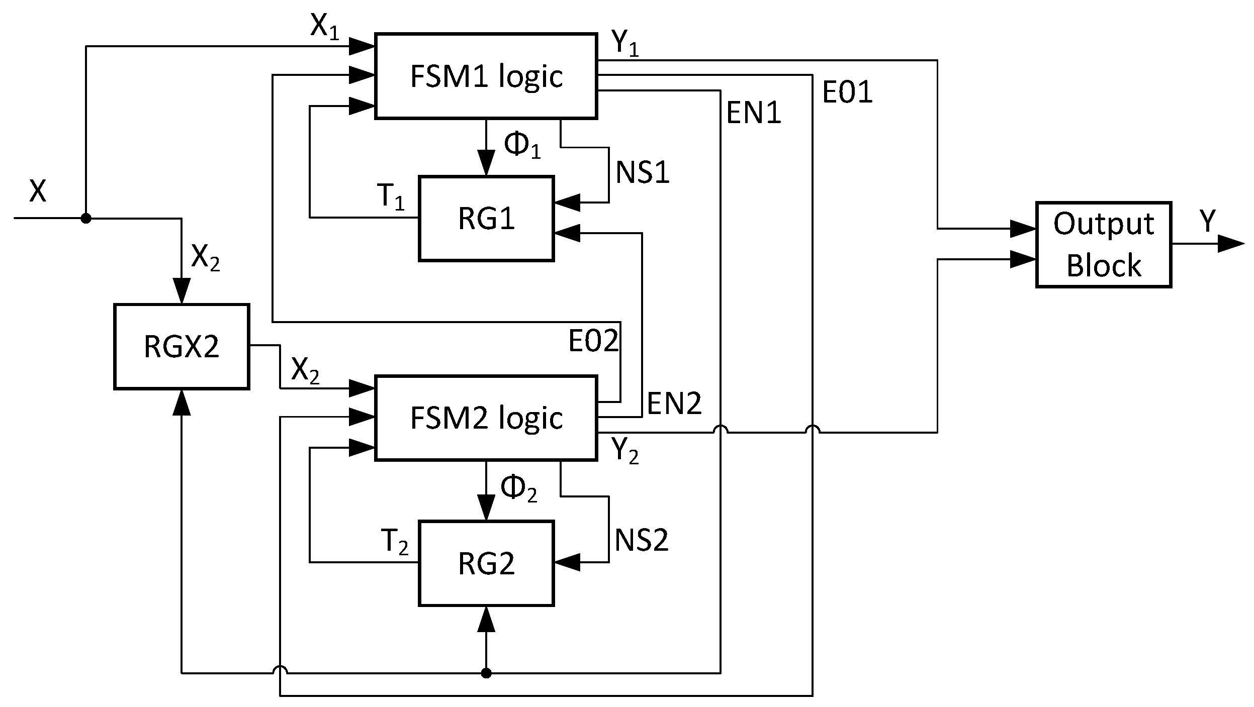
Let us discuss the FSM architecture based on the general decomposition. The FSM circuit includes three combinational blocks and two registers keeping the state codes of different FSMs (
Figure 11).
The set A is decomposed by two disjoint sets, and . The states are encoded using state variables, which form a set . The value of is determined by . The states are encoded using state variables, which form a set . The value of is determined by . There are elements in the set of IMFs ; there are elements in the set of IMFs . Both registers have the same pulses Start and Clock. The set of FSM inputs is represented as . It is quite possible to have identical elements in these sets.
As follows from
Figure 11, the following SBFs should be implemented:
For FSMs based on (
12), the following design method is proposed in [
3]:
Select disjoint subsets and .
Generate STGs for each sub-FSM. Add additional RESET states into each STG.
Copy all transitions from the initial STG in unmodified form into new STGs.
Replace the transitions where and by the two following transitions: and .
Replacing the transitions where and by the two following transitions: and .
In [
3], this approach is combined with clock gating for both inputs and state registers. This combines approaches from [
76,
77] with some new approach. The initial FSM is divided into two FSMs: FSM1 and FSM2.
FSM1 is small; it includes states
with very high probabilities of transitions
where
. This FSM corresponds to the famous 20% of operators determined by [
75]. All other initial FSM states belong to the set
. FSM1 is mostly active, and FSM2 is mostly idle. As a result, it is possible to disable the flip-flops of RG2 and RGX for FSM2. If FSM1 is idle, its state register RG1 can be disabled too. This idea leads to the structural diagram shown in
Figure 12.
The following sets can be obtained from
Figure 12: sets of inputs
and
which can have common elements; sets of outputs
and
which can be disjoint; disjoint sets of IMFs
and
; disjoint sets of state variables
and
; sets of internal control signals (ICSs)
and
. These last sets are the following:
and
. Using the ICS
, FSM1 may disable both RGX2 and RG2. The signal
determines the required state of FSM2. The same function is executed by FSM1 using outputs
. The signals EN1 and EN2 disable the registers of FSM2 and FSM1, respectively. Also, the signal EN1 disables the loading of inputs
into
.
In [
3], the authors show results of experiments conducted using the CAD system SIS [
36] and library [
82]. The results show that the “impressive power savings correspond to larger FSMs (for example, 79.5% for the benchmark
planet)”. There is no gain for small FSMs. This can be explained by adding some circuitry and two extra states. For example, around 30% of the area is added to the FSM circuit implementing the benchmark
planet.
Each FSM of a decomposed circuit can be treated as a superstate (SS). For example, the structural diagram from
Figure 12 corresponds to the STG shown in
Figure 13.
We divided the sets into two subsets each. For example, the set causes transitions inside FSM1 with the generation of outputs . The set causes transitions into the RESET state of FSM2. These transitions are accompanied with the generation of ICSs from set Because the transitions are determined by FSM states and inputs, then it makes sense to use clock gating for both states and inputs.
As shown in [
70], the approach similar to [
71] has two drawbacks:
The decomposed network always includes only two FSMs.
The blocks of clock logic are synchronized, and Clock pulses enter these blocks. As a result, the CL blocks consume a lot of power.
In [
70], an approach is proposed that has the following advantages:
The decomposed FSM is represented by K submachines , where
The blocks of clock logic are asynchronous.
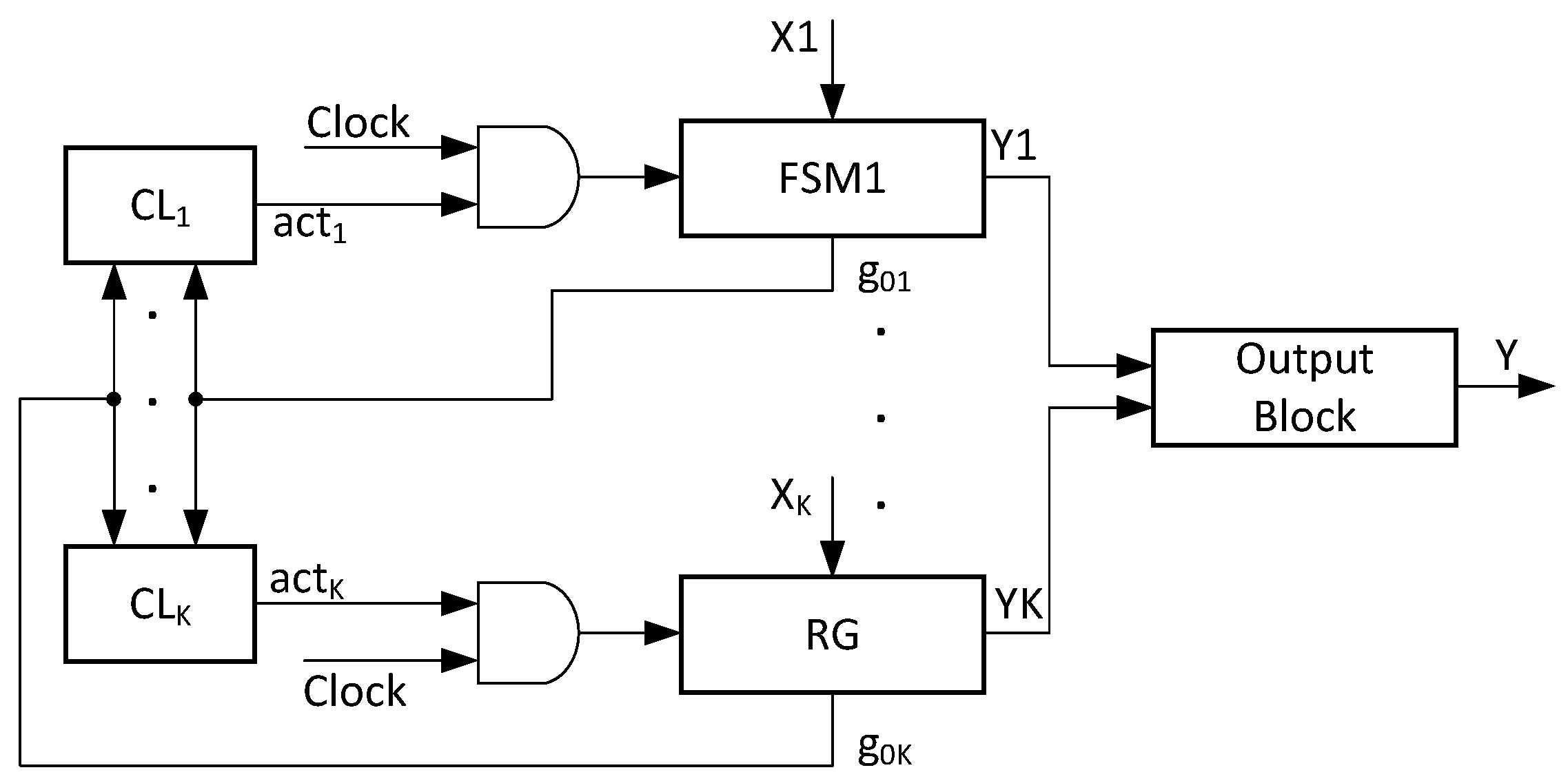
Summarizing the results [
70], it is possible to represent an FSM as a network including
K interrelated partial FSMs. Each of them includes its own synchronization circuit of CL. The circuits
are interrelated (
Figure 14).
Special signals
point to the machine
that should be active in the next cycle of
. Using this signal, blocks
generate signals
Only one of these signals are equal to one. This determines the particular active sub-FSM. The ABD gates help to implement the synchronization for sub-FSMs:
In [
71], the clock signal enters the circuits of clock logic. This is the signal with the highest switching activity among all other signals such as FSM inputs, outputs, and state variables. If the pulse
Clock enters the circuits of CL, then the power consumption is increased as compared with the case discussed in [
70].
As shown in [
70], there are three operating modes for clock logic blocks. During a transition between different sub-FSMs (hand-over mode), all CL blocks are active. In this mode, the maximum amount of power is consumed by these blocks. If
, then the block
is in the disable mode. It means that the power is consumed only by AND gate. The third mode is connected with enabling the block
(
). The circuits of clock logic are passive; no power is consumed. Of course, switching AND gates requires some power.
The asynchronous approach allows a significant saving in power consumption compared with the synchronous approach. As shown in [
70], the power consumption is 1.36 times less for the hand-over mode, 4.13 times less for the enable mode, and 5.9 times less for the disable mode. Also, the difference in power consumption is greater (for different modes).
In [
70], experimental results are shown based on the use of the proposed approach for benchmarks
bbara,
dk512,
ex1,
keyb,
styr,
donfile,
tma, and
scf. They show that for the rather simple benchmark
dk512, the value of
provides the best solution. At the same time, the best result for the not too complex benchmark
ex1 is connected with
. The most complex benchmark is
scf (
,
,
). But the best solution for this benchmark is provided by splitting it into only two interrelated FSMs (
). The same occurs for the simplest FSM represented by the benchmark
bbara, having the following characteristics:
,
, and
. Thus, the optimal value of
K does not depend on the number of states,
M, or inputs,
L, or outputs,
N. The results in [
70] show that the optimal value of partial FSMs,
K, depends on the probabilities of interstate transitions.
Also, the results in [
70] indicate that saving power is connected with the overhead. The conclusion is the same as for other discussed methods: the more complex an original FSM is, the smaller the relative overhead area added. The same is true for the decomposed FSM performance: the more complex the original FSM is, the smaller the impact of additional circuitry on the performance is.
5. Saving Power by State Assignment
A huge number of state assignment methods are known. Some of them are aimed solely at power consumption reduction. But if some method minimizes the chip area occupied by an FSM circuit, then this method minimizes the static power consumption too. Due to this fact, we do not separate these two groups of methods. To prepare this part of our survey, we used the following sources: [
83,
84,
85,
86,
87,
88,
89,
90,
91,
92,
93,
94,
95,
96,
97,
98,
99,
100,
101,
102,
103,
104,
105,
106,
107,
108,
109,
110,
111]. Of course, this is only the tip of the iceberg, but the generalization of these methods gives a general idea of executing RPC through the state assignment.
The power consumption depends significantly on the chip area occupied by an FSM circuit. This was proven, for example, in [
109]. In [
109], four different state assignment approaches are investigated: binary (with
), one-hot (with
), two-hot, and JEDI (the output-dominated version).
In the case of two-hot state assignment, no more than two code bits can be equal to one, simultaneously. This allows the use of less than M bits for the state codes. If , for example, then three bits are required to encode the states. The following codes are used: 001, 010, 100, 101, 011, and 110. This gives the same value of R as it is for the binary state assignment. But if , then four bits are necessary to create two-hot state codes. This is less than for the one-hot approach (), but more than for the binary approach ().
In [
109], the benchmarks from [
82] were used. The benchmarks were represented in the KISS format. The FPGA Express by Synopsis and Xilinx Foundation Tools F3 were used to obtain FSM circuits. The KISS files were transformed into a VHDL-based representation. To obtain the circuits’ characteristics, the authors used the following FPGA sample: XC401EPC84-1. The characteristics were measured using the following operating frequencies: 100 Hz, 2 MHz, and 8 MHz.
was used for the FPGAs of XC401E/XL [
112].
The occupied area was measured as a number of CLBs. This approach is still used nowadays [
113]. Sometimes, the number of used flip-flops is added to the number of CLBs. Some results of the investigations in [
82] are shown in
Table 1.
We selected the results of experiments for five benchmarks having a wide range of characteristics. The last row of
Table 1 includes the numbers of inputs, L, outputs, N, and states, M, of particular FSMs. The number of state variables, R, is the same as the number of flip-flops. It was taken from the reports generated by the CAD tools.
As follows from
Table 1, the number of inputs influences significantly the area characteristics. For example, practically the same value of R is obtained for benchmarks
ex4 and
kirkman. But there are two times more CLBs in the circuit for
kirkman. This is connected with the significant difference in the values of L for these two benchmarks.
The following conclusion is made in [
109]: “For FSMs with up to 8 states, the binary encoding must be used. For FSMs with more than 16 states, the one-hot is always the best choice”. We think this is true if FSMs have the same number of inputs
. Otherwise, a lot depends on the value of
.
It is very interesting that “for any state encoding, the power is linearly correlated with the number of states. The coefficient of correlation is over 0.85” [
109]. The same is true for the relationship “number of states-area”.
Also, there is a very important conclusion made in [
109]: “between area and power, there is the coefficient of correlation 0.91”. It is shown in [
109] that “the 77% of smaller circuits consume lower power”. The results of [
109] show that “area, time and power consumption correlation with other FSM parameters (inputs, outputs and states) and combinations of these parameters neither produce significant results”.
As shown in [
109], the proper state assignment can give up to 57% of power saving. Of course, this is true only for the investigated benchmarks and that particular FPGA chip. The saving amount can be different for a different suite. It is interesting that the discussed methods do not use probabilities of interstate transitions. If we take them into account, we can reduce the switching activity,
. To do it, some special state assignment methods are used.
One of the first algorithms decreasing the switching activity was proposed in [
85]. It targets a state assignment that minimizes the switching activity and takes into account the issue of area. Due to this integral approach, both types of power consumption, static and dynamic, are optimized. The method is based on a probabilistic description of FSMs.
The method uses an average switching activity to find the switching (transition) probability. This allows the obtainment of the probabilities of FSM interstate transitions. This information is used for executing the state assignment. But to do it, it is necessary to have the input switching probabilities. In [
85], an STG is modeled as a Markov chain [
114]. The Markov chain model describes an STG as a directed graph with weighted edges and a structure isomorphic to the initial STG. The STG is transformed into a weighted undirected graph. The weight of each edge is proportional to the total probability of a transition between FSM states
connected by this edge. This final STG is used as the initial information for the state assignment step.
The main idea of [
85] is “to find a state assignment that minimizes the number of state variables that change their values when the FSM moves between two adjacent states”. In the best case, only a single state variable is changed, as it is for Gray codes. But
state variables are necessary for the Gray state assignment. The aim of [
85] was to find the value of state code bits close to the minimum value defined by (
4).
A state encoding is represented by a Boolean matrix. Its rows correspond to state codes and columns to state variables. The required state assignment can be found by the solution of the integer linear programming problem formulated in [
85].
For small FSMs, it is possible to find the exact solution. For complex FSMs, only a suboptimal solution can be found because the problem is NP-complete. Thus, there are a lot of heuristic algorithms for its solution [
90,
91,
115]. In [
85], the column-based approach is used. In this case, each state variable corresponds to a column. The method includes R iterations, when each state variable
receives either zero or one. The assignment is done in a way that minimizes the switching activity. The algorithm tries to minimize the number of different values of state variables for states with the highest switching probabilities. The algorithm produces a semi-exact solution.
To minimize the chip area, some additional constraints are used. Additional metrics are used, similar to the ones proposed in [
90]. One of them is a fan-out-oriented metric. It can be used for FSMs with a small number of inputs and a large number of outputs. The second metric is a fan-in-oriented metric. It can be used for FSMs with a large number of inputs and a small number of outputs. These area constraints are added as weights for an STG.
To reach some trade-off for area–power, the parameter
is introduced in [
85]. It shows what is more important for a given task. The weight
of an edge connecting states
and
is determined by
The weights for area (
) are determined using the MUSTANG approach [
90]. The weights for power (
) are determined by the heuristic algorithm from [
85].
The results of experiments with the benchmarks from [
82] show that the saving power increases with the growth in FSM complexity. If
, then the maximum saving is up to 8%; if
, the maximum saving is up to 16%; if
, then the maximum saving is up to 25%. Thus, adding one to R improves the power consumption by approximately 8%. Also, the growth in the number of state variables, R, leads to reducing the area overhead. It means that applying similar approaches makes sense for rather complex FSMs.
Using [
85] allows the creation of the block diagram shown in
Figure 15. In this algorithm, we assume that pairs
are created for FSM states. These pairs include states
such that there is at least a single transition between these states (either
or
). Each pair has a weight
The block diagram is shown in
Figure 15.
In the beginning, it is necessary to organize a queue of pairs . The pairs are placed in the queue in the descending order of weights The algorithm has no more than steps.
Every step is connected with the following operations. The ith pair is selected from the queue (block 3). The pair includes some states and . If state has no code (the output “No” from block 4), then we check whether state has a code (block 5). If there is a preliminary selected code (the output “Yes” from block 5), then we should select the best possible code for state (block 7). The best possible code is selected from still “free” state assignments. The best code should have a minimum possible Hamming distance (HD) with the code . Next, the value of i is increased by one (block 9). If the queue is not empty, then the selection process is repeated (the transition to block 3). Otherwise, the process is terminated. If there is still no code for state (the output “No” from block 5), then the selection of the best codes for both states is executed.
If already exists (the output “Yes” from block 4), then we check for code (block 6). If there is no code (the output “No” from block 6), then a possible best code is selected (block 8). Otherwise, no codes should be selected, and the process is repeated (go to block 9).
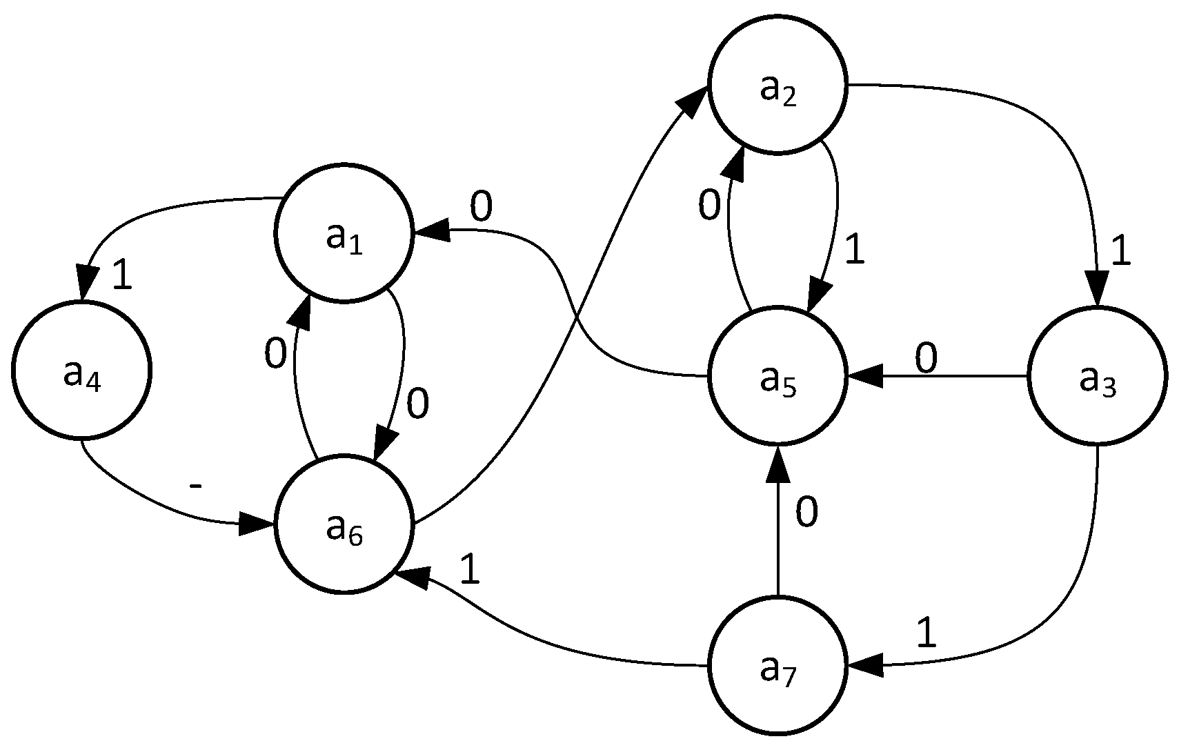
Consider the following example. Consider the set
for some FSM
These states form the following I = 9 pairs:
,
,
〉,
,
,
,
,
, and
. R = 3 and
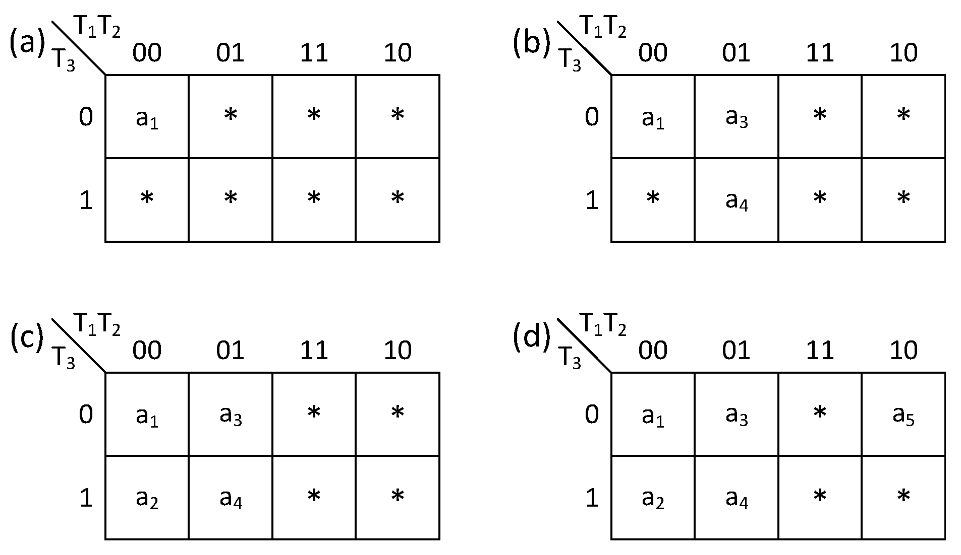
. Now, we should find the best state codes using the algorithm shown in
Figure 15. The process of state assignment is shown in
Figure 16.
The start point of the state assignment process is shown in
Figure 16a. The code 000 is assigned to the initial state
. All other cells of the Karnaugh map contain the asterisk signs.
- Step 1.
The first pair of the queue is selected. This the pair
. To encode the states
, we should select codes with a minimum number of ones, and
. This means, the actions from block 11 are executed. The codes of
are shown in
Figure 16b.
- Step 2.
Now, the pair
is selected. Because the transition state
is already encoded, the action from block 7 is executed. The best possible solution is shown in
Figure 16c.
- Step 3.
The pair is selected. Both states from this pair are encoded. Thus, no new codes are assigned during this step.
- Step 4.
The pair
is selected. Now, the code for
should be selected. This corresponds to block 8. The final solution is shown in
Figure 16d.
This algorithm belongs to the group of “greedy” algorithms. It makes the optimal choice at each step. The algorithm does not change already selected codes. As a result, such a solution is not optimal. It can be improved.
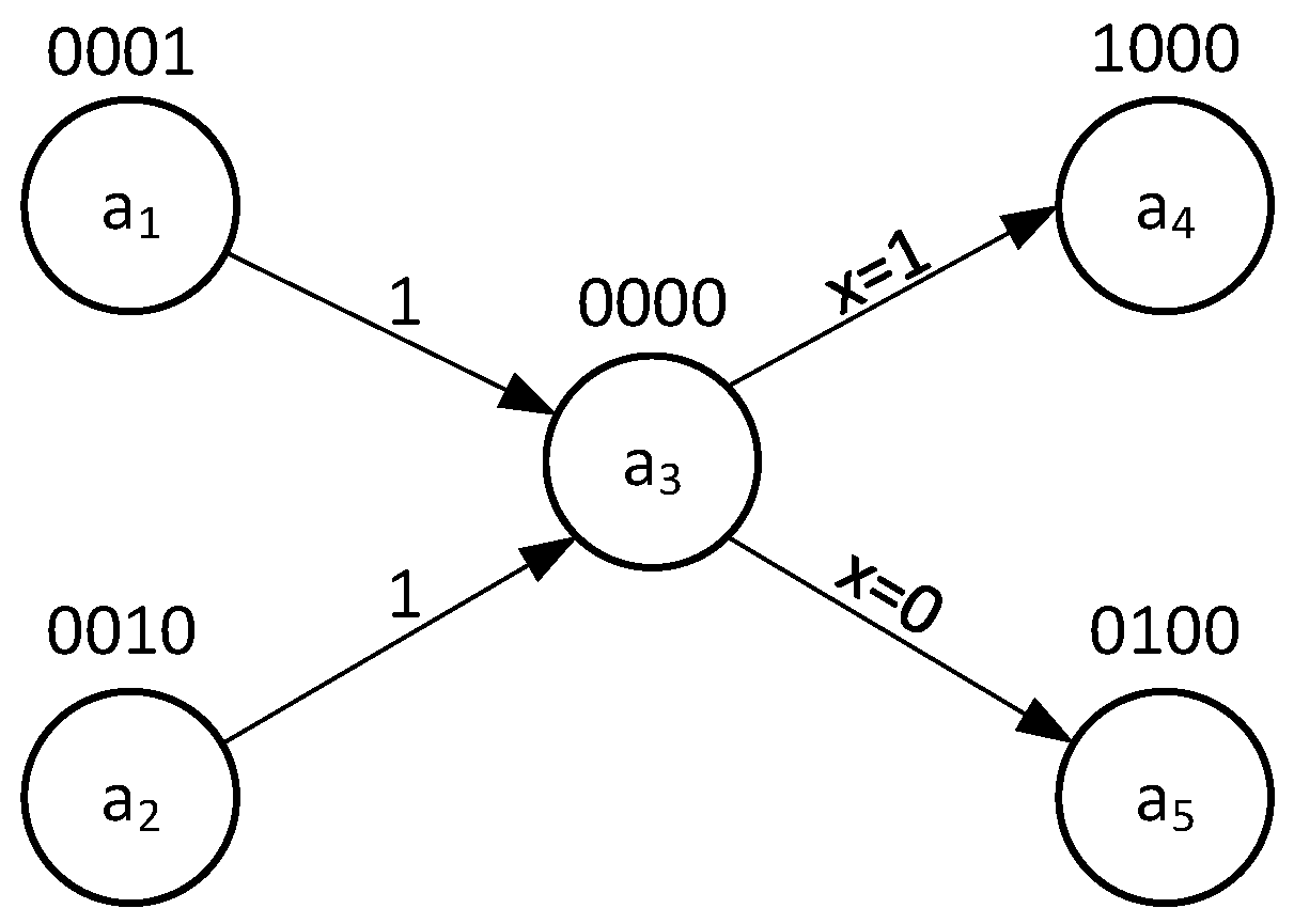
Consider what causes the overhead for this algorithm. For example, an STG includes the subgraph shown in
Figure 17a.
If
, then the algorithm [
85] will select the codes
and
. Because the code
is now fixed, there is a limited choice of possible codes for
. To provide HD = 1, the algorithm can assign the code 010 to
. These codes provide the best solution from the greedy algorithm’s point of view.
But this approach does not take into account LUT counts for the output logic. As follows from
Figure 17a,
. If an FSM circuit is implemented with LUTs having three inputs, then two LUTs are necessary to implement the circuit for
(
Figure 17b). This circuit has two levels of LUTs and six interconnections.
If a JEDI-based style of state assignment is used, then the states
and
will have adjacent codes. If, for example, there is
and
, then it gives the Boolean equation
. The corresponding circuit has only a single LUT, a single level of logic, and four interconnections (
Figure 17c).
Thus, for the discussed case, the JEDI-based circuit is faster and requires fewer LUTs. This is quite possible that the circuit from
Figure 17c has better power characteristics than its equivalent shown in
Figure 17b.
The following conclusion can be made from this example. To find a desirable trade-off among power consumption, area, and performance, it is necessary to take into account the output logic too. There are special resynthesis methods [
116] that can improve the overall quality of an FSM circuit. They are out the scope of this survey.
Let us only point out that the resynthesis allows a reduction in the number of logic levels and simplifies the interconnection system. These two issues are very important in the LUT-based design [
116].
As mentioned in [
117], many systems of emerging computing and communications equipment are control-dominated. The controllers are mostly implemented as FSMs. Because many devices are mobile, then a RPC is a very important issue. In the case of controllers, it is very important to decrease the power consumption, because “controllers are always active. As a result, a good amount of system power is consumed by the controllers” [
117]. This explains the necessity of RPC for FSMs.
The RPC can be achieved by adding states [
95] or adding bits to state codes [
108]. These additional states and bits can also be viewed as the power overhead.
We start from the state splitting approach [
95]. The approach takes its roots in 1963 [
118]. This approach was used for optimizing FSMs [
119] and minimizing the number of FSM states [
120]. Also, it can improve the power consumption.
Consider a part of an STG (
Figure 18a) taken from [
95]. The state codes are shown near the graph nodes.
To reduce the switching activity,
, it is necessary to diminish the value of the Hamming distance. In the best case, HD = 1 for all pairs
existing in a particular STG. Obviously, each state code can have only R adjacent state codes with HD = 1. The state
(
Figure 18a) is connected with R + 1 = 4 states. HD = 1 for the pairs
,
, and
. But HD = 2 for the pair
.
It is possible to “split” the state
into two equivalent states
and
. These states have the same transitions. Now, each of the new states (
and
) has exactly R adjacent states. If the state codes are the ones shown in
Figure 18b, then HD = 1 for all existing adjacent state pairs (
,
,
,
,
, and
.
Each state
can be characterized by two sets. The set
includes states
, such that there are transitions
. The set
includes states
, such that there are transitions
. As follows from
Figure 18a, the following sets can be formed:
and
. The splitting state
makes sense because the following relations hold:
and
. This means that the splitting can be executed if
For states of transitions, state codes depend on the codes of previous states. As a result, there are a lot of splitting options. It is necessary to choose the option leading to the maximum RPC.
In [
95], two algorithms are proposed for the state splitting. In the first case, all possible splittings are investigated for states satisfying (
15). This approach requires the extensive search of an optimal solution. In the second case, only two subsets are formed for
. One subset includes a state
having the maximum probability of transition into the state
to be split. The second subset includes states
. This solution is a suboptimal one.
In [
95], experimental results are provided. They were obtained using the library [
82] and the software package ZUBR [
121]. The results show that a RPC takes place for 27 benchmarks (57.4% of all benchmarks).
The results [
95] show that the proposed approach reduces the power consumption by an average of 6.92%. At the same time, the maximum RPC is equal to 81.02% (for the benchmark
tma). The simplified algorithm produces solutions very close to optimal. The average difference is around 0.08%.
Consider
Figure 18a.
and
;
. As follows from (
15), it is impossible to assign adjacent codes to all states included into the set
. If the number of state variables is greater than what is defined by (
4), then the condition (
15) is violated. In this case, there is an optimum solution shown in
Figure 19.
The analysis of
Figure 19 shows that the following relation holds:
. The codes (
Figure 19) provide the minimum power consumption for this part of the STG. But they add a power overhead since
instead of
. It means that there is an additional flip-flop and additional loading for the clock tree.
A method [
108] based on this idea was tested using the benchmarks from [
82]. The outcomes of this approach were compared with results obtained for NOVA, JEDI, and a column algorithm [
85]. The experiments were conducted for the following conditions:
= 5 V,
= 5 MHz,
= 3 pF.
The approach from [
108] allowed a reduction in the power consumption by a factor of 1.7 (NOVA), 1.36 (JEDI), and 1.12 (column algorithm). For example, in the case of benchmark
tbk, adding one to the minimum value of R diminished the power consumption by 34%. Of course, it is necessary to take into account the influence of increasing the number of state variables on both area and time characteristics of a resulting FSM circuit.
All discussed methods of state assignment have the same specificity: a state code
is assigned to the state
as an R-bit string during some step of the state assignment process. In [
122], a method is proposed where each state assignment step gives only a single bit of state codes.
The method [
122] reduces the switching activity,
. But at the same time, it diminishes a chip area occupied by an FSM circuit. The decomposition strategy of the state assignment is proposed in [
122]. The approach produces a binary tree whose leaves correspond to state codes.
As presented in [
122], we explain this approach using the benchmark
[
82]. The benchmark’s STG is shown in
Figure 20.
The state assignment [
122] starts by calculating the probabilities
of interstate transitions. To get the total probabilities of transitions
, the product of probabilities
and
is calculated. The value of
determines a probability that the FSM is in the state
. For
, the following values of
are used:
,
,
,
,
,
.
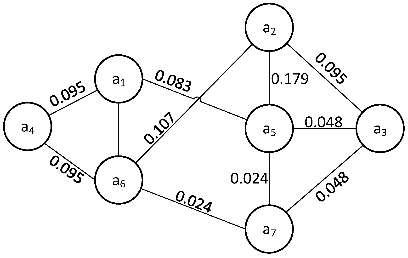
The summation of the direct edges’ probabilities for each pair of states produces an undirected graph with edge weights (
Figure 21). Now, it is necessary to minimize the Hamming distance between the codes
and
with the high transition probability.
Using the algorithm [
122] gives the binary tree for
dk27 (
Figure 22). The values zero and one correspond to state code bits. To find the code, we should move from the leaves to the tree root.
The resulting state codes are shown in the Karnaugh map (
Figure 22b). R = 3 (this is the number of tree levels). For example, the following codes can be found:
,
, and so on.
To optimize the power consumption, it is necessary to take into account dependencies between states at some level of the tree. The optimization can be performed by swapping the nodes on the same tree level. It results in changing values of bit codes. For example, swapping state codes
and
(
Figure 22a) produces state codes
and
.
As shown in [
122], the state assignment (
Figure 22b) gives a sum of all Hamming distances equal to 16. Also, it gives a switching activity equal to 1.357. After swapping codes for pairs of states
and
, the sum is equal to 15 and the average switching activity is equal to 1.19. Obviously, the less switching activity there is, the less the power consumption.
In [
122], some results of experiments were shown. The system SIS [
36] was used to calculate power consumption. The results were compared with results obtained using one-hot approach, JEDI, NOVA, and the one-level tree (OLT) algorithm [
83]. The calculations were performed for the benchmarks from [
82], with
= 5 V and
= 20 MHz.
The results of these experiments showed the following values of power consumption and area (
Table 2).
These results show that the method in [
122] provides the minimum power consumption for the benchmarks from [
82]. At the same time, the minimum area is provided by JEDI. The worst area characteristics are provided by the one-hot approach, whereas the maximum power is consumed by NOVA.
We can evaluate the overall efficiency of an algorithm by finding the product “Area × Power”. In the discussed case, the following values of this product were found:
for one-hot,
for JEDI,
for NOVA,
for OLT, and
for [
122]. A comparison these products show that both JEDI and [
122] produce practically the same results.
All discussed state assignment methods are deterministic. To optimize power consumption in FPGA-based circuits, it is necessary to minimize the switching activity of flip-flops. This reduces the dynamic power consumption. To reduce the static power, it is necessary to reduce the chip area occupied by an FSM circuit. The chip area is determined by the number of LUTs and their interconnections. As noted in [
92], the deterministic algorithms “are far from being optimal”.
To improve the power consumption, various nondeterministic evolutionary methods have been developed. A survey of them can be found, for example, in [
94]. All these methods deal with NP-complex problem, where NP stands for nondeterministic-polynomial time [
123].
In [
124], a genetic algorithm is proposed. For a given FSM, the algorithm optimizes the chip area occupied by its circuit. To get the optimal result, this algorithm uses a fitness function to evaluate the resulting chip area. In another genetic algorithm [
125], the authors use literal counts as a cost function. In [
93], both literal count (for area) and switching probability (for power) are used as an approximate cost function. In [
111], the genetic algorithm optimizes both static and dynamic power consumption. To do it, the algorithm uses a fitness function based on the number of product terms, the switching activity, and Hamming distance among pairs of state codes. In [
87,
126], a genetic algorithm tries to optimize both static and dynamic power consumption. In [
127], a multiobjective genetic algorithm optimizes both the area and power. To create a fitness function, it uses the number of product terms, the switching probability for state pairs, and the Hamming distance among pairs of states.
Some algorithms are based on simulated annealing for optimizing area and/or power. In [
128], the approximate fitness function is used to optimize the area. In [
129], both area and power are optimized. To do it, a fitness function is based on three characteristics: (1) the number of product terms, (2) the switching probability for state pairs, and (3) the Hamming distance. Also, approaches such as binary particle swarm and cuckoo search are used for optimizing the static power consumption (the circuit area) [
130,
131]. In [
92], a probabilistic swap search state assignment algorithm is proposed. It is based on (1) assigning probabilities of each pair of code swaps and (2) probabilistically exploring pairwise code swaps. As a result, both area and power consumption are minimized for multi-level FSM circuits.
As follows from this short analysis, the outcome of state assignment significantly influences the power characteristics of FSM circuits. In this survey, we mostly analyzed FPGA-based FSMs. As a rule, LUT-based FSM circuits are multi-level. To decrease the static power, it is necessary to diminish the number of literals in SBFs (
5)–(
6). This allows a reduction in the chip area occupied by an FSM circuit. To reduce the dynamic power consumption, it is necessary to optimize Hamming distances between state codes for pairs of states with a high switching probability.
6. Replacing LUTs by Embedded Memory Blocks
As we have shown before, even a single EMB can replace a lot of LUTs and interconnections (
Figure 5). To optimize the resulting FSM circuit, it is necessary to find a configuration
which allows us to obtain a single-level EMB-based FSM circuit. In this case, there are very important relations among the EMB characteristics (
) and FSM parameters (L, N, and R). The LUT count of a LUT-based FSM circuit is not important for replacing LUTs by EMBs.
An EMB is a coarse-grained element compared to a LUT. Thus, the transition from LUT-based FSMs to EMB-based FSMs is a transition from fine-grained to coarse-grained elements. This is similar to the transition from radio components (transistors, capacitors, resistors, inductors, and so on) to integrated circuits. Such a transition improves the final product quality (reducing the size, increasing the performance, reducing the power consumption, increasing the reliability) by reducing the number of interconnections. Also, there is a simplification of complex tasks such as the mapping, placement, and routing. Thus, we can expect the same effect from replacing LUTs by EMBs.
All EMB-based FSM design methods originate in microprogram control units (MCUs). The idea of MCUs was proposed in 1951 by M. Wilkes [
132,
133]. The MCUs have been used to control the process of program execution in computers. The MCU design methods depend on the approach used for addressing the microinstructions (MIs). One of the first addressing methods is compulsory addressing [
134,
135].
To design an MCU circuit, it is necessary to represent an initial STG as a microprogram. A microprogram is an ordered set of microinstructions kept into a special control memory (CM). A microinstruction location into CM is determined by its address. A format of an MI with compulsory addressing includes four fields [
134]. The field
includes a code of the collection of outputs (COs) executed in a particular cycle of MCU performance. The field
includes a code
of an FSM input
to be checked for determining the transition address. The field
includes a transition address for the case when
. The field
includes a transition address for the case when
. For unconditional transitions, the field
is empty; in this case, the next address is determined by the contents of
.
The following rule determines the next microinstruction address:
In (
16),
is a cycle time,
is the next address (an address of an MI executed in the cycle
),
,
,
are the contents of the corresponding fields in the current operation cycle,
is a value of an FSM input determined by the field
. The unconditional transition is determined by the first line of (
16).
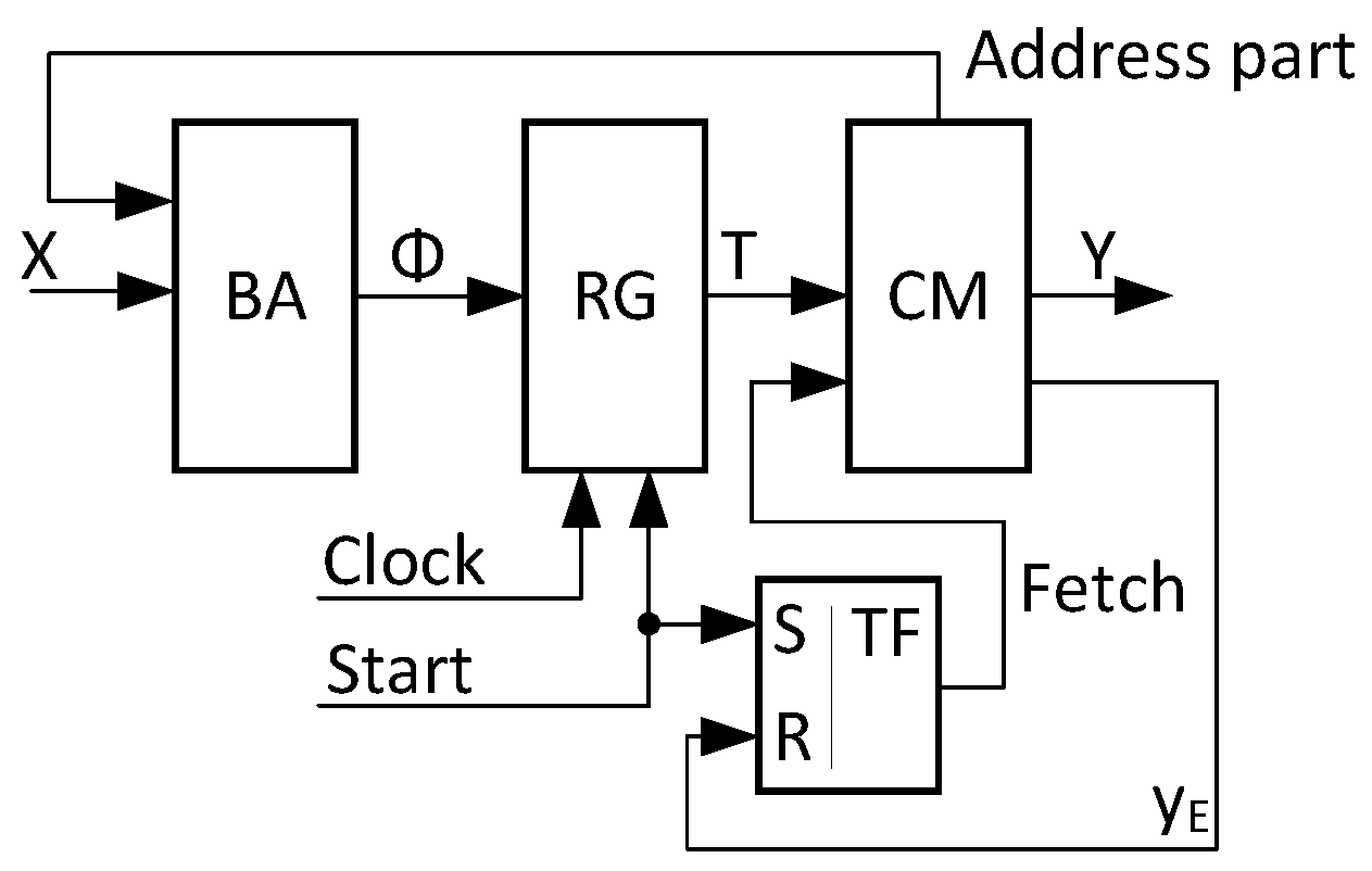
The following blocks represent the circuit of an MCU with compulsory addressing: block addressing (BA), register of microinstruction address, RG, control memory, and control flip-flop (TF). A structural diagram of an MCU is shown in
Figure 23.
The MCU (
Figure 23) operates in the following manner. If
, then (1) the first address of the microprogram is loaded into RG and (2)
. If
, then the current MI is read from the CM. At the instant
t, a microinstruction
is fetched from CM. Its field
is transformed into outputs
. They enter other blocks of the digital system. The address part of MI (fields FX, FA0, FA1) enters the BA, together with new values of FSM inputs. According to (
16), BA generates variables
representing an address of the MI to be executed in the next cycle of MCU operation. The process is terminated if
. In this case,
, and it is impossible to read MIs from the control memory.
In the first MCUs, the CM was implemented using read-only memory (ROM) blocks. The circuit of BA is implemented using gates and multiplexers [
134]. If a microprogram includes M microinstructions, then the number of address bits is determined by (
4). Obviously, the following relation holds:
.
In the case of FPGA-based FSMs, the analog of the CM is implemented by EMBs, the analog of the addressing block is implemented using LUTs and dedicated multiplexers [
46]. There is a significant difference between ROMs and EMBs. Namely, EMBs are synchronized blocks having a special control input which can be connected with the pulse
Clock [
46]. Thus, there is no need to have a separate register of addresses. The RG is hidden inside an EMB. Also, an EMB has a special control input to generate the zero code on its outputs. This input can be connected with the pulse
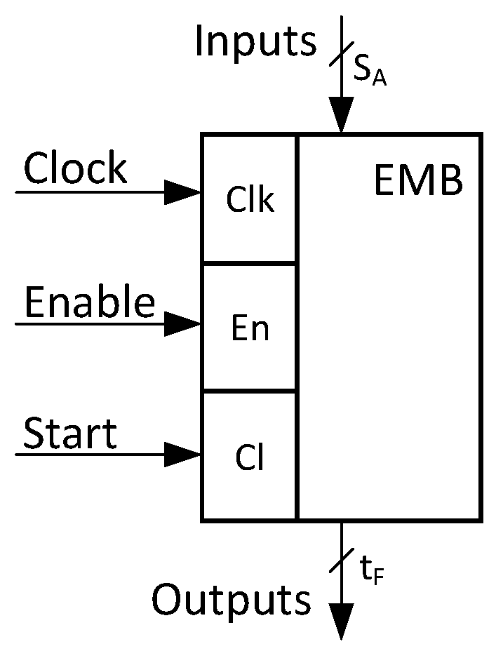
Start. A typical EMB has
address inputs,
cell outputs, and three control inputs
(
Figure 24).
If Clock = 1, then the outputs of a cell determined by the address inputs are loaded into the internal register of EMB. If Clear = 1, then RG = 0, and the address inputs are ignored. If Enable = 0, then the EMB operates in its standard mode. If Enable = 1, then the EMB outputs are in the third state. This means that the EMB is not connected with other existing blocks.
In [
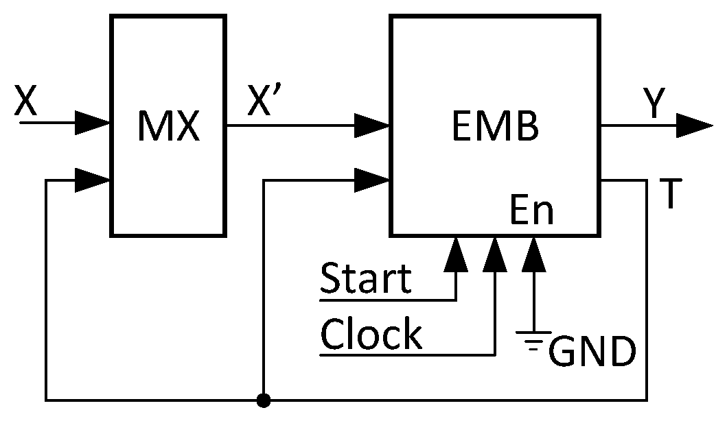
46], the authors propose to use EMBs for implementing Mealy FSM circuits. They propose an approach when the input MX cuts off the “don’t care” FSM inputs (
Figure 25).
In [
46], the authors show that using EMBs instead of LUTs allows a reduction in the power consumption. They write that “although memory arrays have greater power consumption when compared to individual LUTs and flip-flops, for state machine which uses several flip-flops, LUTs, and significant routing resources, the EMB-based approach has lower power consumption”. In
Figure 25, the pulse
Clock is connected with the
input of EMB, the pulse
Start is connected with
, and
.
The results of experiments are presented in [
46]. They were obtained using the chip XC2V250-6fg256 by Virtex-II (Xilinx) and the library of standard FSM benchmarks [
82]. To calculate the main characteristics of the FSM circuits (the number of EMBs, LUT counts, and power consumption), the authors used an experimental flow based on the CAD tool SIS [
36]. This flow is shown in
Figure 26.
Using an initial STG, SIS generates a net-list of an FSM in
format. This file describes the combinational circuit represented by (
5)–(
6) and the FSM state register. This file is transformed into a VHDL program using the translator from
to VHDL. The tool Simplify-pro by Sinplicity executes the technology mapping. As a result, an
file is generated. It describes LUTs, FFs, and their interconnections. To execute the placement and routing, they use the Xilinx ISE 4.2.03i design tool suite. To calculate the power dissipation, the
file enters Xpower tool. This tool also uses the
(value change dump) file produced by ModelSim simulator. These files are used to estimate the power dissipation.
The results of the experiments in [
46] show that using EMBs leads to a significant area and power consumption improvement. The area was measured as a mutual LUT count and the number of flip-flops.
Table 3 includes the results of experiments on some of the benchmarks from [
82].
The power was measured for different clock frequencies. But in
Table 4, we show only results obtained for 100 MHz. The column “%” includes the percentage of power saving due to the replacement of LUTs by EMBs.
Also, in [
46], the authors propose to enable the EMB input for further power saving. If an FSM does not change its state (this is an idle state), then the pulse
Clock is disconnected from the synchronization input.
To save power, it is necessary to add some LUT-based logic for the timing control. For Mealy FSMs, this block is synthesized using some inputs
, where
, and some outputs
, where
. The outputs can be used for situations where a state is not changed, but outputs are changed. This situation is shown in
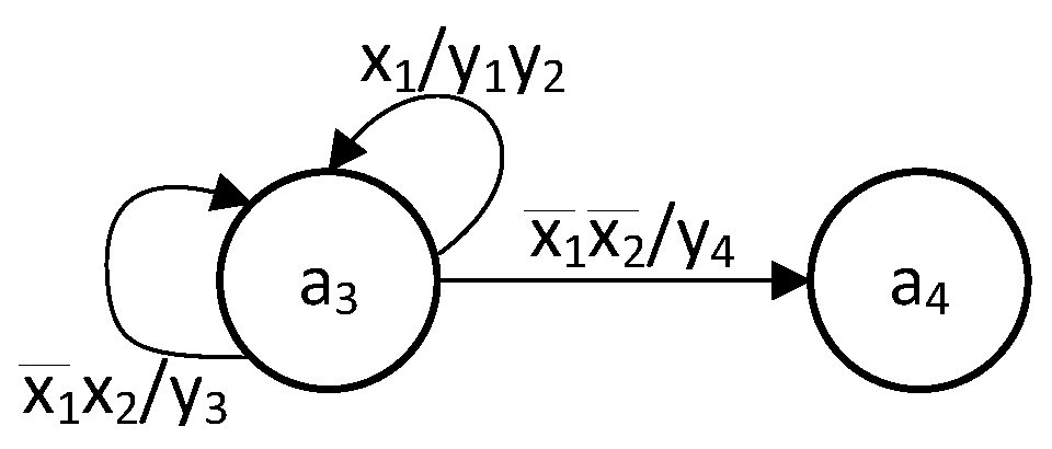
Figure 27.
As follows from
Figure 26, the state
is not changed if there is either
or
. But during these idle cycles, different collections of outputs are generated:
and
.
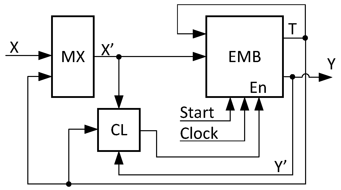
The EMB-based Mealy FSM with the enabling
Clock is shown in
Figure 28. The block CL represents the clock logic. This block generates the function
As shown in [
46], using CL allows a reduction in the power consumption compared with the Mealy FSM shown in
Figure 25. But this approach is connected with the power overhead: the CL adds delay in performance and increases LUT count. Both saving power and area overhead are shown in
Table 4.
In
Table 4, the column “%” includes power saving for the frequency equal to 100 MHz. This saving takes into account the power consumed by the block CL. As follows from
Table 4, using EMBs and CL allows a saving from 4% to 26% compared with equivalent LUT-based FSMs. Of course, these numbers are valid only for these experiments’ conditions. But this approach may be used if the power saving is the most important issue of a particular project.
There is no need for the input register RGX for EMB-based FSMs. Due to the existence of the internal register inside EMB, the outputs are registered. The registering outputs have the same positive effect as the registering inputs . In both cases, the FSM outputs are stable. Also, using EMBs has a clear advantage over LUT-based approach. Namely, there is no need for using additional LUTs to create the input register RGX.
Using EMBs makes sense only till there is no need for the cascading EMBs. Let the symbol
stand for the number of address inputs if
. The cascading should be used if the following condition holds:
This is quite possible than more than a single EMB is used for implementing an FSM circuit (even if (18) is violated). In this case, it is necessary to compare the characteristics of equivalent LUT- and EMB-based FSM circuits. Also, a mixed approach should be investigated too. In the case of a mixed approach, a circuit is represented as a network of LUTs and EMBs [
22,
48,
49,
50,
51,
52,
53,
54].


