1. Introduction
Since the introduction of 5G mobile communication technology, various studies have been actively conducted to apply beamforming technology to various communication and radar systems [
1,
2,
3,
4]. Unlike previous technologies, such beamforming technology requires a plurality of transceivers. Accordingly, the importance of compact size and low power consumption techniques in transceivers is increasing [
5,
6]. Therefore, in the beamforming system, it is common to design transceivers using a complementary metal-oxide semiconductor (CMOS) process with the highest degree of integration among various semiconductor process.
In general, in the case of RF transceivers, it is advantageous to use a high current consumption and a high trans-conductance,
gm to ensure a high frequency operation, so a general-power (GP) CMOS process is more preferred than a low-power (LP) CMOS process. In particular, transistors with high
gm are advantageous in securing high output power as well as high power gain in the CMOS power amplifier. In addition, if the power gain increases with the increase in the
gm of the transistor, the number of amplification stages required by the CMOS power amplifier decreases, which helps to improve the efficiency of the CMOS power amplifier. However, the LP process is more preferred for reducing power consumption of various digital and analog circuits for controlling RF transceivers [
7]. Particularly, in the beamforming systems, LP processes help minimize DC power consumption in digital and analog circuits that deal with relatively low power. Accordingly, the GP process and the LP process may be used at the same time to obtain low power consumption of the digital and analog ICs, compact size, high performance and low power consumption of the RF transceiver; however, in this case, the entire transceiver may not be implemented as an integrated circuit (IC). Therefore, there are often cases in which RF circuits also use the LP process for integration with digital and analog circuits.
In terms of high frequency circuits, the LP process has a number of disadvantageous factors in terms of power gain, output power, efficiency, and noise figure. However, in order to reduce the weight of the entire transceiver, research on high-frequency circuits, such as CMOS power amplifiers, variable gain amplifiers, attenuators, phase shifters, switches, and low-noise amplifiers using a LP process is essential.
In this study, a K-band power amplifier was designed with a multi-stage structure using the LP CMOS process. In order to overcome the low
gm of the LP CMOS process and secure sufficient gain, the CMOS power amplifier was designed as a four-stage structure. In addition, to suppress the increase in the area of the entire transceiver due to the increased area of the CMOS power amplifier with the four-stage structure, we propose a structure capable of mounting the 180° phase-shift function of the phase shifter, which occupies a large chip area in the beamforming system, to the CMOS power amplifier. Although the area occupied by the 180° bit in the phase shifter varies depending on the structure, according to previous study, the 180° bit accounts for about 40% of the core size, as inferred from a chip photograph [
8,
9]. However, the proposed CMOS power amplifier does not require an additional area for mounting the 180° phase-shift function.
2. Design of the CMOS Power Amplifier with LP Process
In this study, a power amplifier was designed using a 40-nm LP CMOS process.
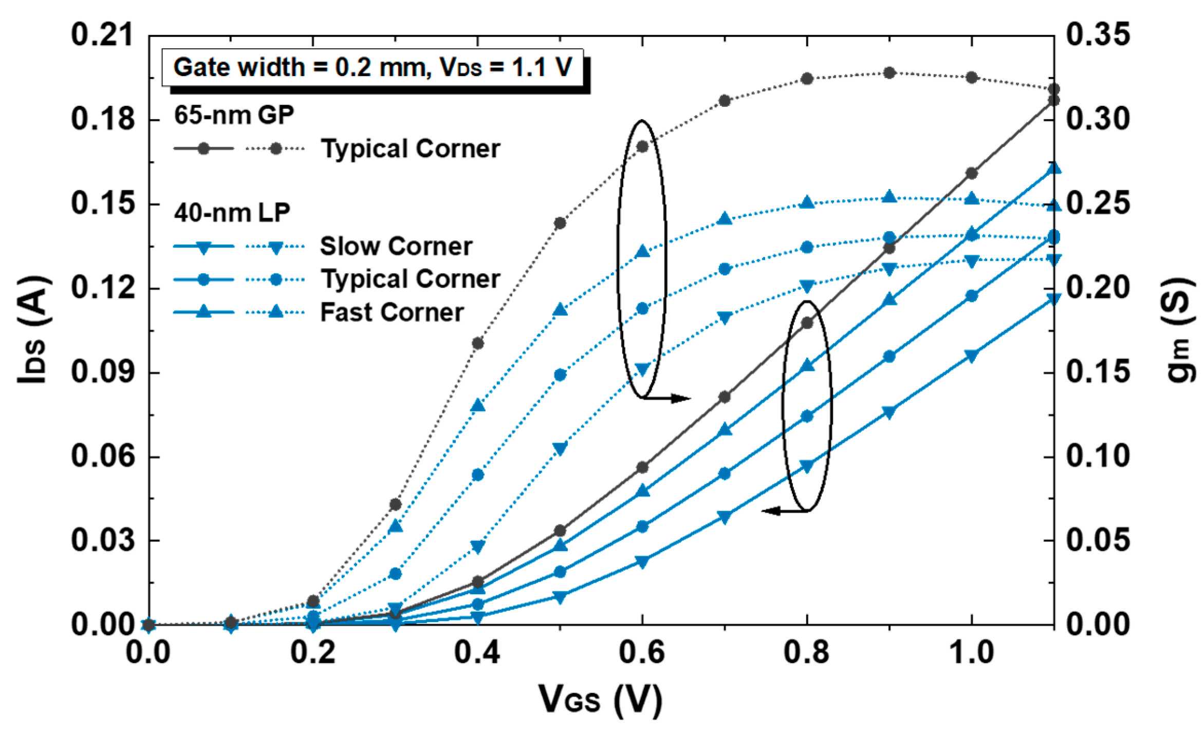
Figure 1 shows the I–V curve of NMOS with the same gate width using the 65-nm GP and the 40-nm LP processes. As shown in
Figure 1, the transistor using the 40-nm LP process has a relatively high threshold voltage, a low current level, and a low
gm value compared to the transistor using the 65-nm GP process.
With the same gate width, comparing the
gm values of the transistors using 65-nm GP and 40-nm LP processes in
Figure 1, the 40-nm LP transistor has a
gm value of approximately 66% compared to that of the 65-nm GP transistor. Therefore, when the 40-nm LP process is used to obtain the same gain as the two-stage power amplifier using the 65-nm GP process, a three-stage structure is required. In a simple calculation, to obtain the same gain from the power amplifier, in the case of the 40-nm LP process, the required IC area is increased by approximately 33% compared to the 65-nm GP process. Furthermore, a low current level of the 40-nm LP process compared to the 65-nm GP process causes a low output power of the power amplifier. In order to obtain the required output power, sufficient drain current is required, and, to this end, an LP process-based power amplifier should use an increased transistor size. However, the increased transistor size also increases parasitic capacitances, which requires high driving power, resulting in a decrease in gains and an increase in dc power consumption. Furthermore, the low
gm of the LP process-based transistor directly degrades the gain of the power amplifier. Such characteristics of the LP process act as unfavorable factors in terms of power gain, output power, and efficiency of the power amplifier.
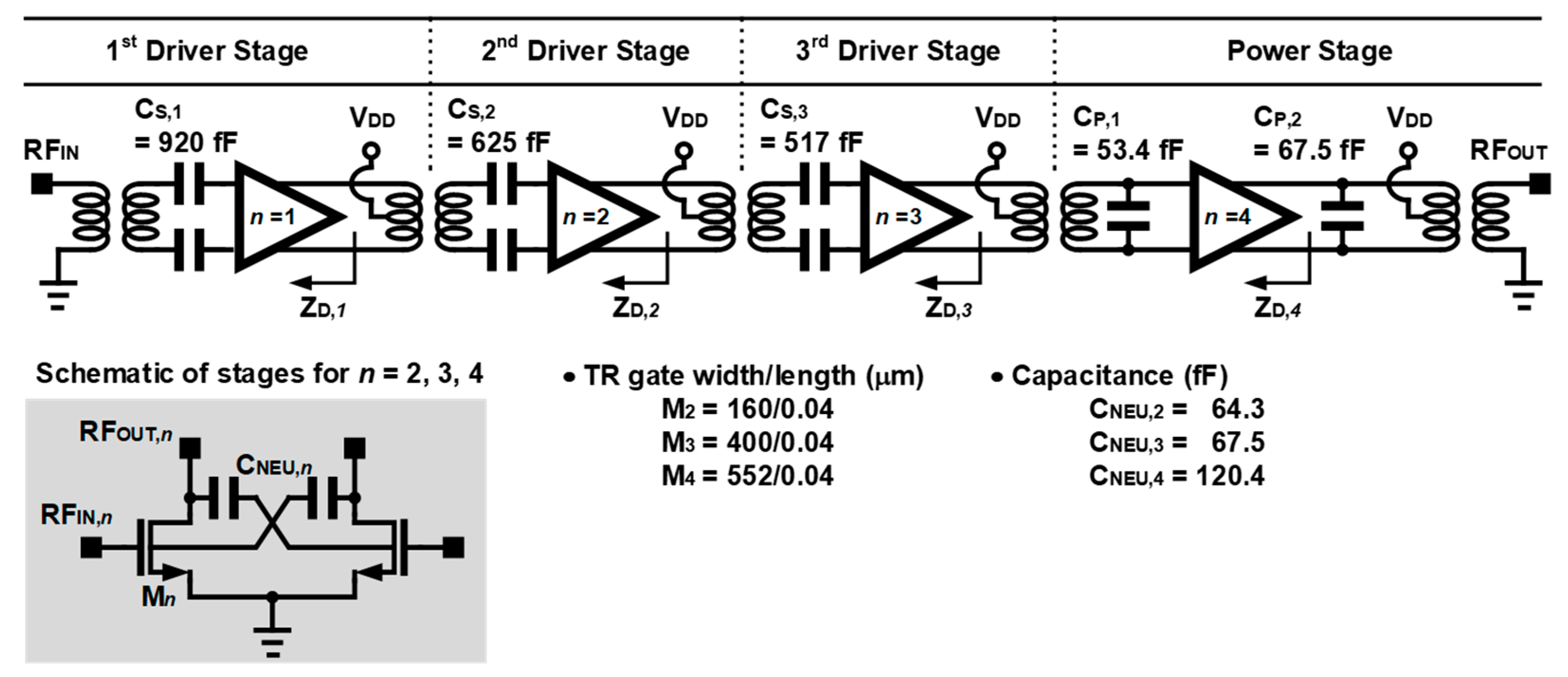
Among them, in particular, due to the low gain characteristics of the LP process, it is essential to apply a multi-stage structure in the power amplifier using the LP process. In this study, four stages were used, as shown in
Figure 2, to secure sufficient gain of the power amplifier. As shown in
Figure 2, the power amplifier is designed using a differential structure to obtain virtual AC ground [
10,
11,
12,
13]. Accordingly, transformers as a function of input and output baluns were essentially used in the input and output matching networks [
14]. In addition, the transformer was used for the component of the inter-stage matching networks. The matching networks were completed with the transformers and additional metal–insulator—metal (MIM) capacitors. Second, third-driver and power stages were designed as common-source (CS) structures. The structure of the first driver stage is described in the following section. Additionally, the capacitive neutralization technique was used to secure stability and power gain [
15,
16,
17]. The supply voltage of each amplification stage was entered through the center-tap of the primary winding of the transformer. To obtain accuracy of the simulation, the electromagnetic (EM) simulation was conducted in the design of the passive devices, including transformers and inter-connection lines.
In the power stage of the power amplifier, the power-matching technique was used to improve maximum output power using output transformer and shunt MIM capacitors, as shown in
Figure 2. The used values of the MIM capacitors and transistors of the power amplifier are also shown in
Figure 2.
2.1. 180° Phase Shift Function in the First Driver Stage
As described in the previous section, the power amplifier was designed as a four- stage structure to secure sufficient power gain in the LP CMOS process. However, when the power amplifier is composed of four stages, the overall IC area inevitably increases. In particular, compared with the power amplifier based on the GP CMOS process, the LP CMOS-based power amplifier requires more amplification stage, considering the low gm of the LP CMOS process. The increase in the area makes the configuration of the beamforming system difficult. Therefore, in this study, the 180° phase-shift function, which occupies a large area in the beamforming transceiver, was embedded in the power amplifier to reduce the area of the entire transceiver. The phase-shift function was embedded in the first driver stage with the lowest power handling. Because each stage has a power gain, the power that the first stage deals with is the lowest, and the power increases as it goes to the power stage. Therefore, if the phase-shift function is implemented in the second or third stage rather than the first stage, the size of the transistor for implementing the phase shift function increases, thereby increasing the additional power consumption, causing the power amplifier to lose efficiency. In addition, in extreme cases, if the phase-shift function is implemented in the power stage, the power-matching technique should be implemented simultaneously, which hinders securing the output power of the power amplifier. Accordingly, by embedding the phase-shift function in the first driver stage, it was possible to minimize the power amplifier’s output power degradation due to the embedding of the phase-shift function.
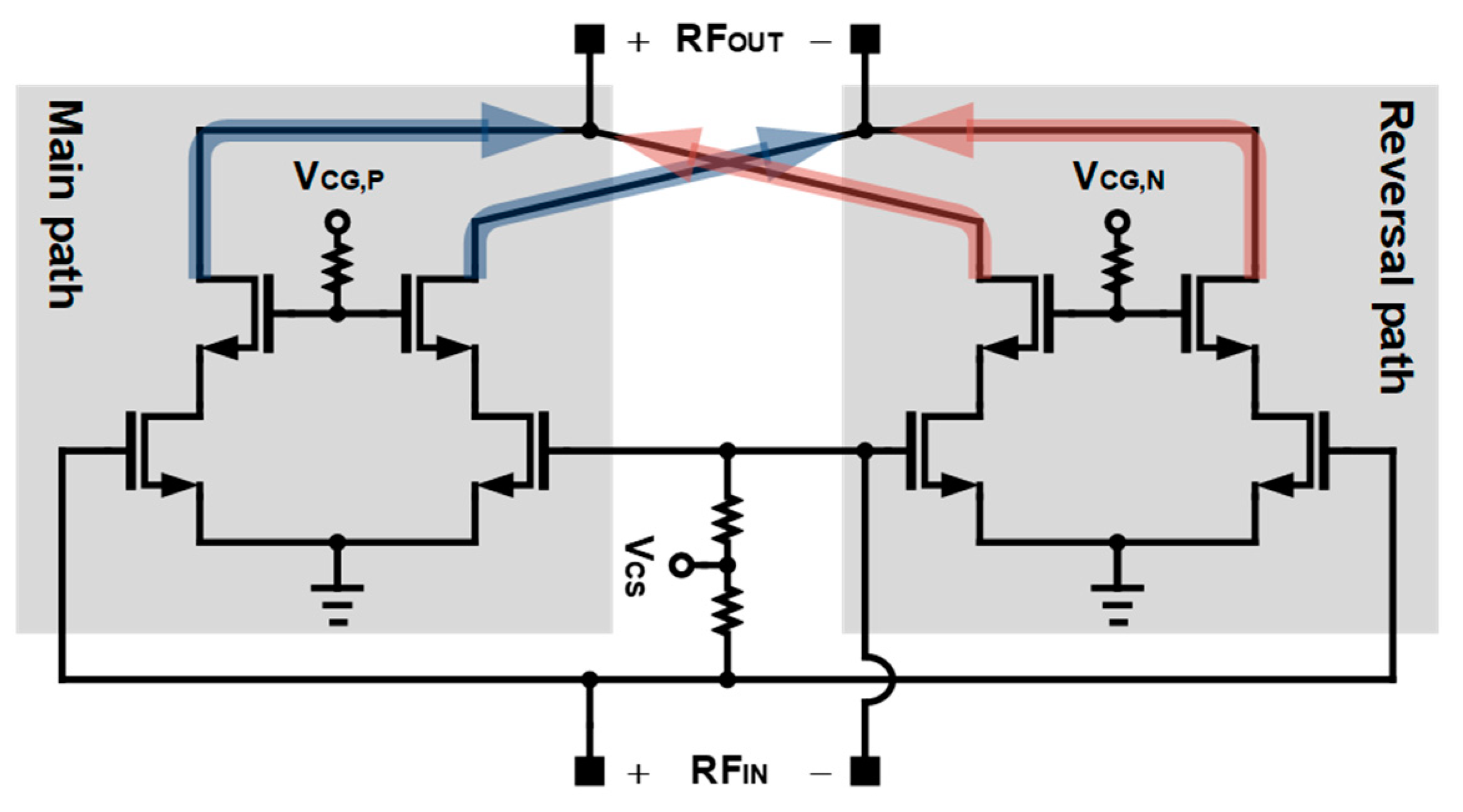
Figure 3 shows the typical schematic of the amplification stage for embedding a 180° phase-shift function [
9]. As shown in
Figure 3, in general, to realize the 180° phase-shift function, two identical amplifiers, which are located in parallel to each other, may be used. In
Figure 3,
VCG,P and
VCG,N were the gate bias of the common-gate (CG) transistors while
VCS was the CS transistor. In the typical structure, one of the two amplifiers is selectively operated by
VCG,P and
VCG,N, thereby implementing the 180° phase-shift function. However, in this case, due to the two amplifiers, the required chip area could increase.
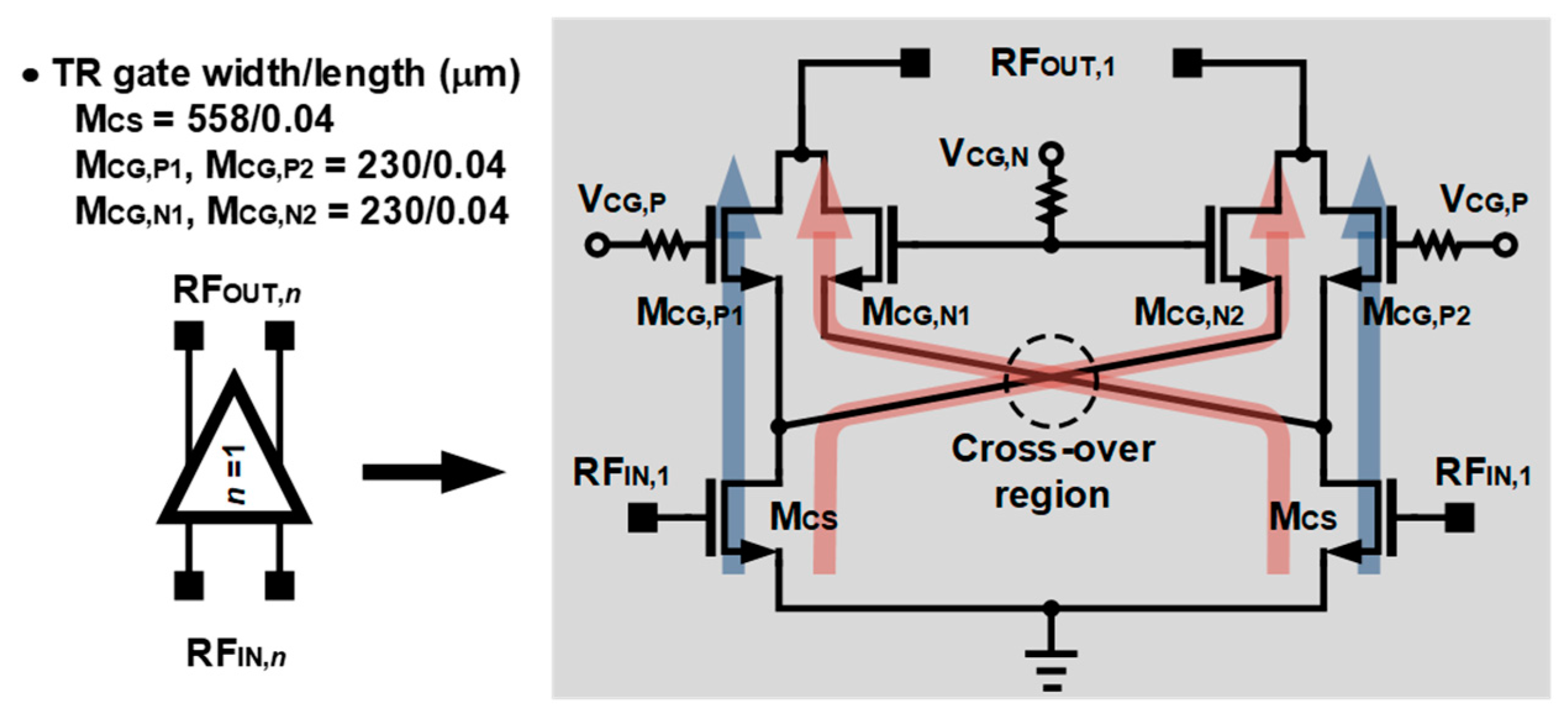
Figure 4 shows the schematic of the proposed first driver stage for embedding a 180° phase-shift function. In this work, considering the overall chip area of the power amplifier, instead of using two identical amplifiers, the phase-shift function was implemented by modifying a single-cascode structure. As shown in
Figure 4, from a general cascode structure, a CG transistor was designed by dividing it into two. M
CG,P1, M
CG,P2, M
CG,N1, and M
CG,N2 were the divided CG transistors. The input signal path was converted to 180°, according to the
VCG,N and the
VCG,P. The
VCG,P (or
VCG,N) was gate bias voltage of M
CG,P1 and M
CG,P2 (or M
CG,N1 and M
CG,N2) As a result, the CS transistor of M
CS operated at all times in the 0° and 180° phase-shift modes. On the other hand, as can be seen in
Figure 4, M
CG,P1 and M
CG,N1 (or M
CG,P2 and M
CG,N2), which are divided-cascode transistors, operate selectively, according to each mode, and consequently perform a phase shift function.
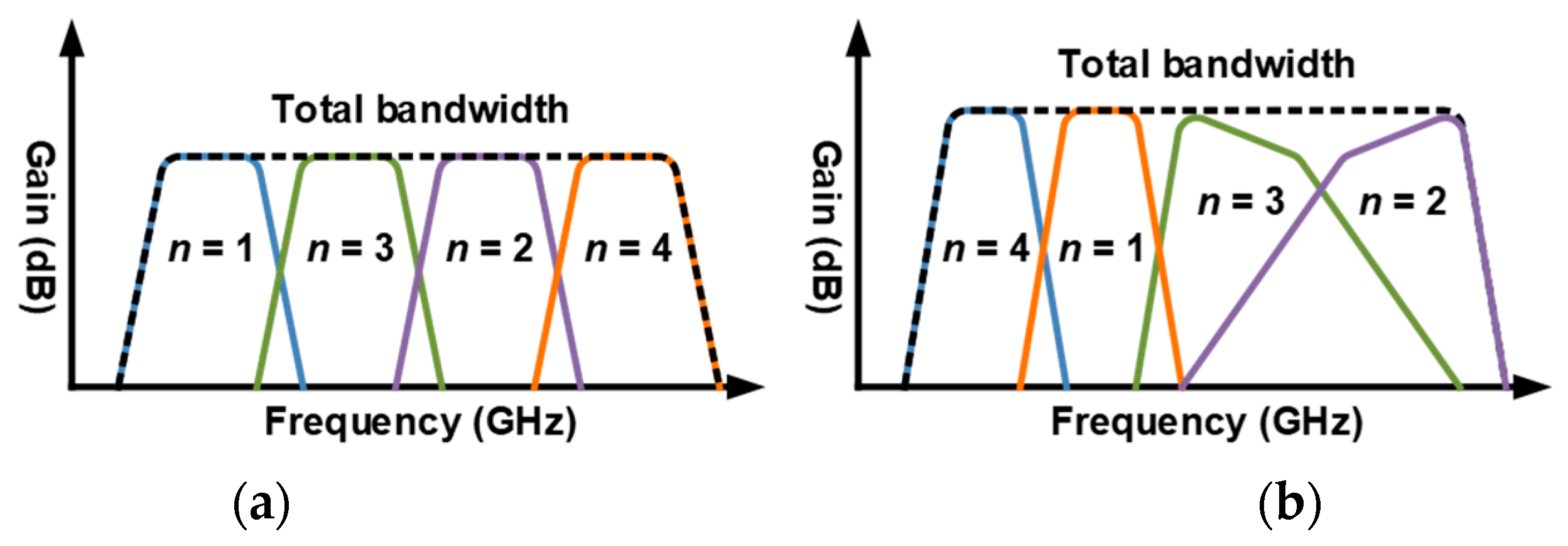
2.2. Multi-Stage Structure for Wide Bandwidth
In this study, wideband characteristics were secured by actively utilizing the four-stage structure. As shown in
Figure 5a, superimposed staggered tuning techniques that optimize each stage to have a different frequency band are typically utilized to secure the wide bandwidth of the power amplifier [
18,
19,
20,
21]. The superimposed staggered tuning techniques have been continuously improving in various ways, such as a superimposed dual-band structure [
22]. In general, the superimposed staggered tuning techniques are mainly applied to amplifiers consisting of two or three stages. In order to apply the superimposed staggered tuning technique to the power amplifier of this study, the characteristics of each stage were first considered. In this study, a power-matching technique was used in the power stage, while the phase shift function was installed in the first driver stage. Therefore, the first driver and the power stages were designed to have a high peak gain at different frequencies rather than to widen the bandwidth. In addition, the first driver and power stages are designed to be responsible for gain in a relatively low frequency. Instead, for the second and third stages, it was designed to have wide bandwidth as well as secure the gains, as it only needs to be faithful to the role of securing the gains. Such wide bandwidth technique is shown in
Figure 5b. The frequency with the highest gain for each stage was optimized though C
S,1, C
S,2, and C
S,3 of
Figure 2.
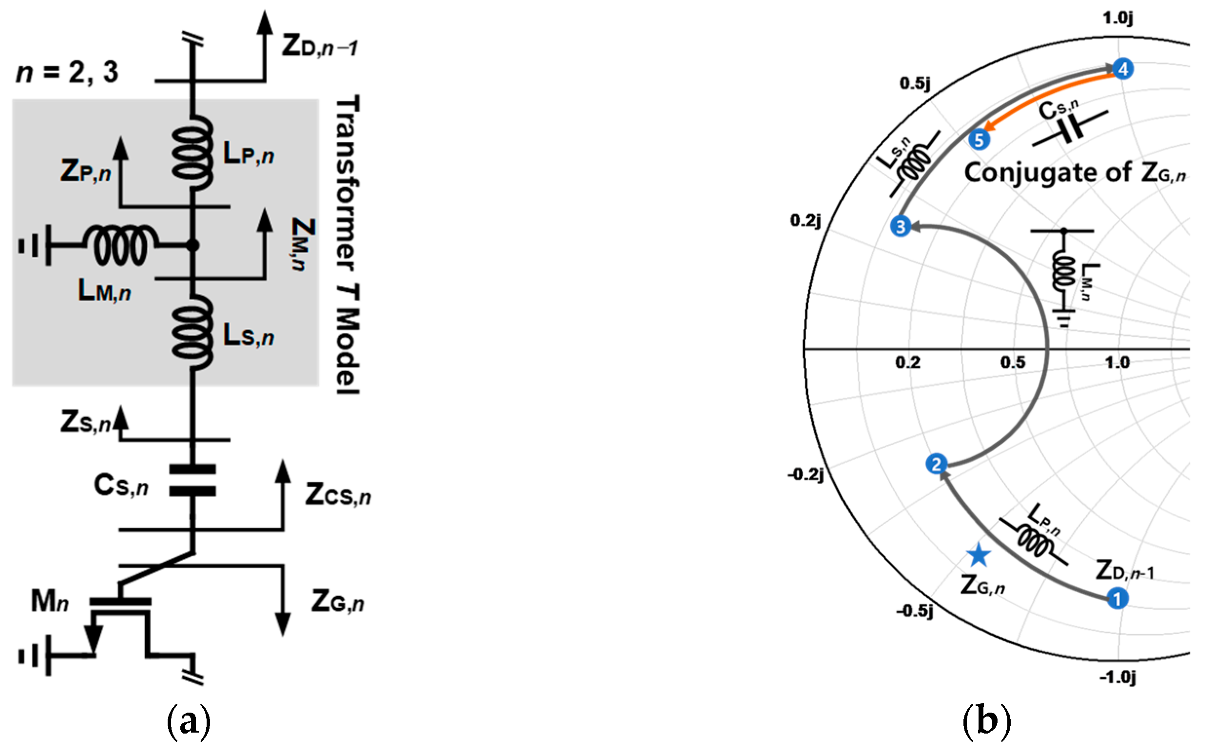
For the driver and power stages, it was designed with the conjugate-matching and the general power-matching techniques, respectively.
Figure 6 shows the locations of impedance of the transistors used in this study. The transformer used for matching for each stage was interpreted as a simple
T-model. In
Figure 6a,
LP,n,
LS,n, and
LM,n show the self- and mutual-inductances of the primary and secondary windings of the transformer, respectively.
Figure 6b shows a part of the Smith chart showing the trajectory of change in impedance for conjugate matching according to the matching components.
3. Simulation and Measurement Results
In this study, we designed a power amplifier for 5G communications using the 40-nm CMOS LP process that provides eight metal layers to verify the feasibility of the proposed structure. The design parameters of the used device are shown in
Figure 2 and
Figure 4.
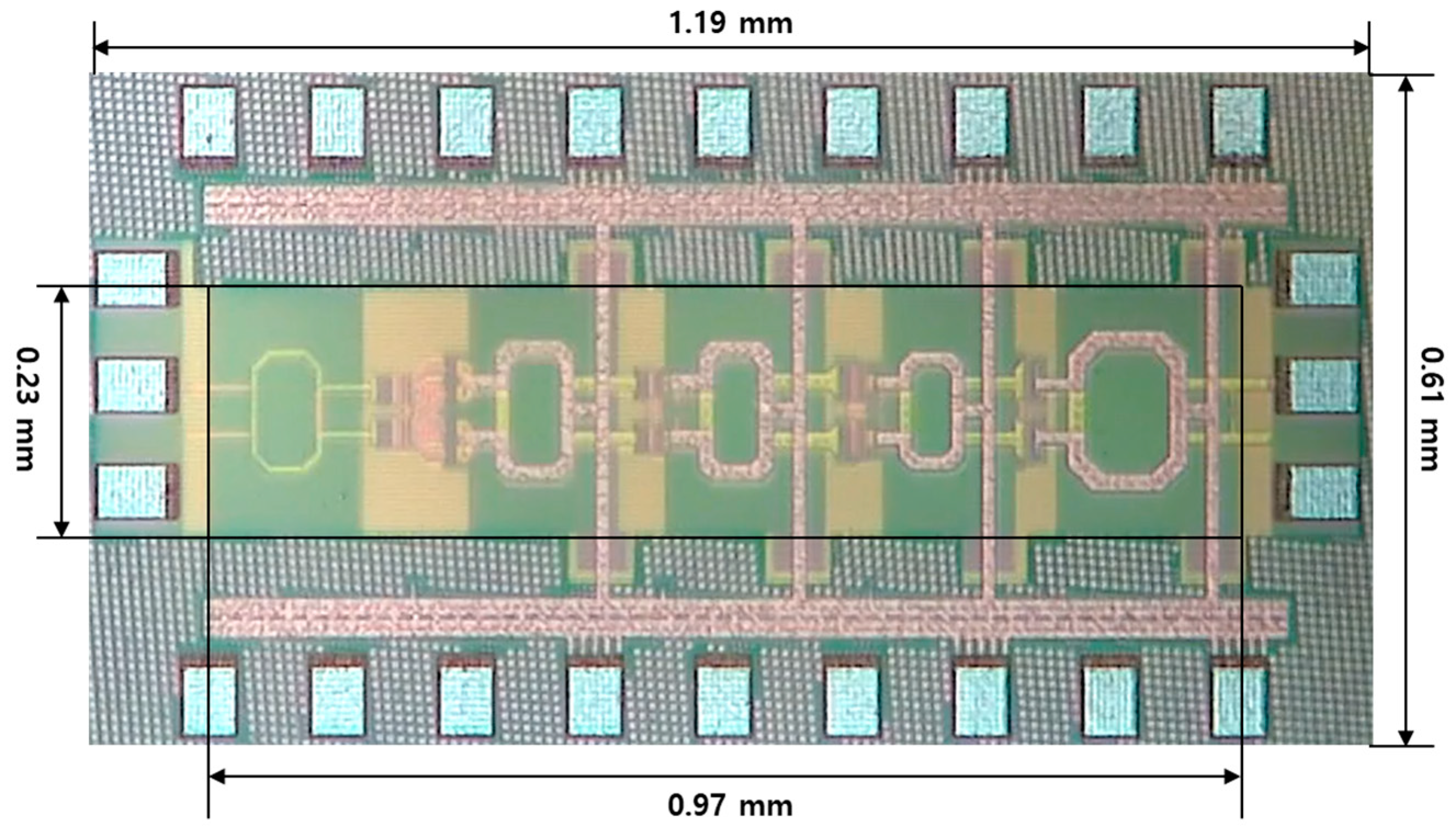
Figure 7 shows a photograph of the designed power amplifier with 180° phase-shift function in the first driver stage. In the chip photograph, the first, second, and third driver stages were sequentially placed from left to right. The power stage is situated on the right-most side in the chip photograph. The chip size was 1.19 × 0.61 mm
2, including all test pads. The core size was 0.97 × 0.23 mm
2, excluding all test pads and decoupling capacitors. To secure AC ground, the decoupling capacitors were placed near the test pads. However, since the power amplifier in this study was designed in a differential structure, the decoupling capacitor played an auxiliary role and the virtual ground of the differential structure was actively utilized for the AC ground. As can be seen in
Figure 7, there is no additionally required chip area for implementing the 180° phase-shift function. The used supply voltage, V
DD, of the designed power amplifier was 1.1 V. In the case of the first stage with the cascode structure for phase-shift function, the gain could be increased by using a higher supply voltage; however, the first stage also used a supply voltage of 1.1 V to minimize the additionally required low-dropout (LDO) regulators.
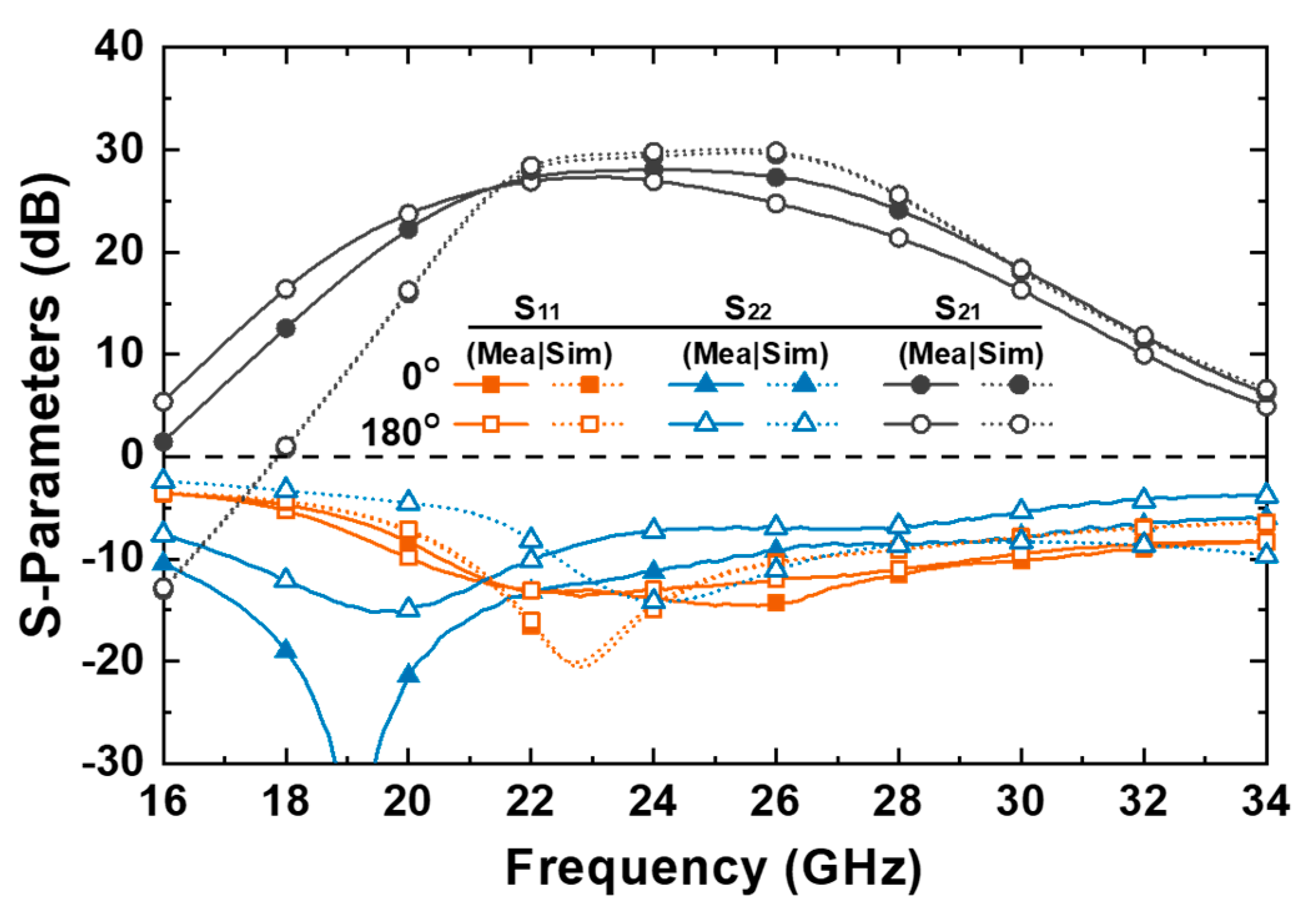
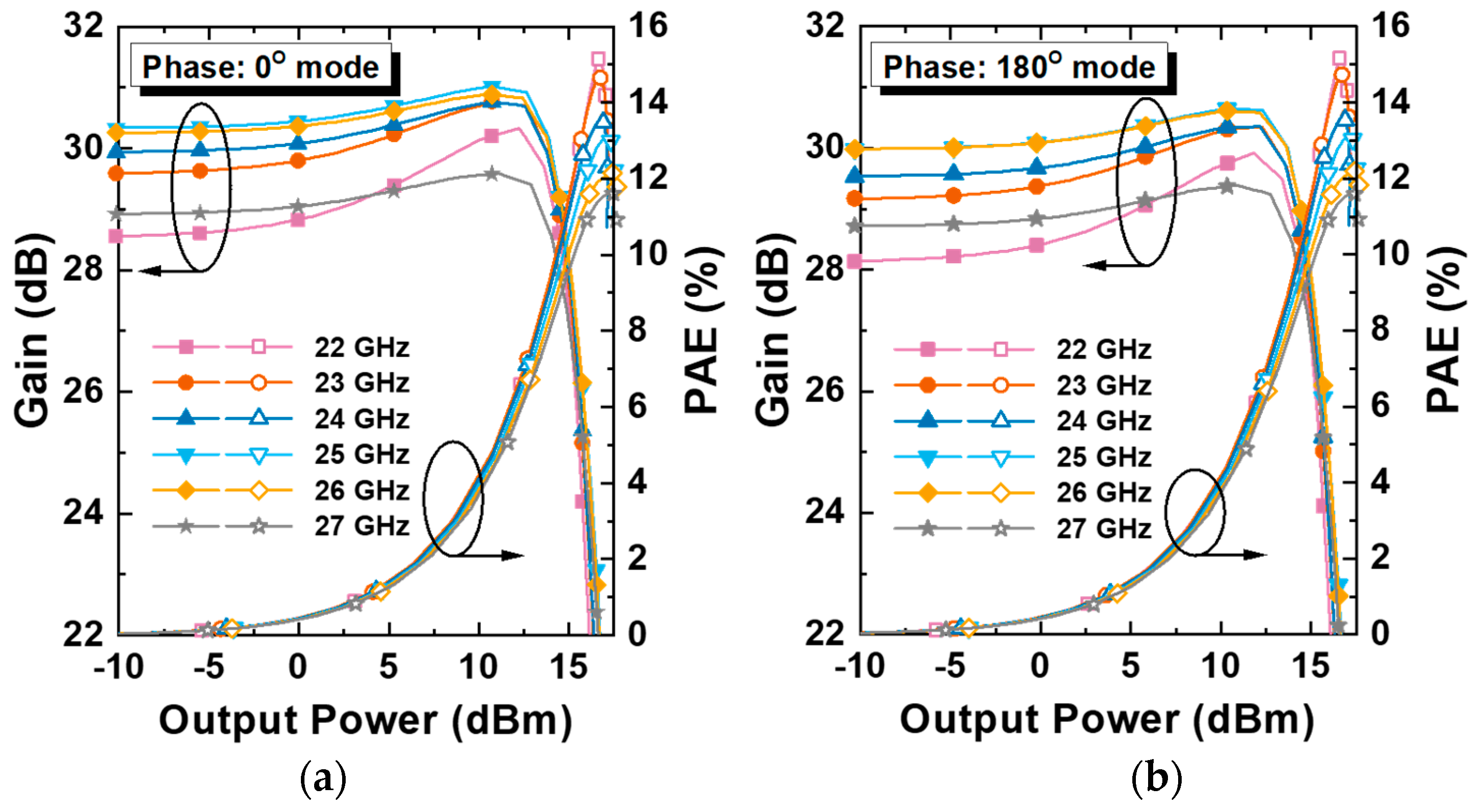
As shown in
Figure 8, in the frequency range of 22.0 GHz to 26.0 GHz, the simulated gain was higher than 28.4 dB and the gain flatness was 1.4 dB or less. Originally, the power amplifier was designed through simulation with a typical corner model. However, in the worst case, the size of the transistor was determined in preparation for being implemented as a slow corner. After measuring the DC current of the power amplifier manufactured in a foundry, it was confirmed that the power amplifier was manufactured as a slow corner. Since the designed power amplifier was made as a slow corner, the simulation results were performed under slow corner conditions. As a result of the simulation of the k-factor, we confirmed that the designed power amplifier was unconditionally stable. In the first stage, with 180° phase-shift function, a difference in measured
S-parameters between 0° and 180° modes occurred due to parasitic components occurring at the cross-over region circled in
Figure 4.
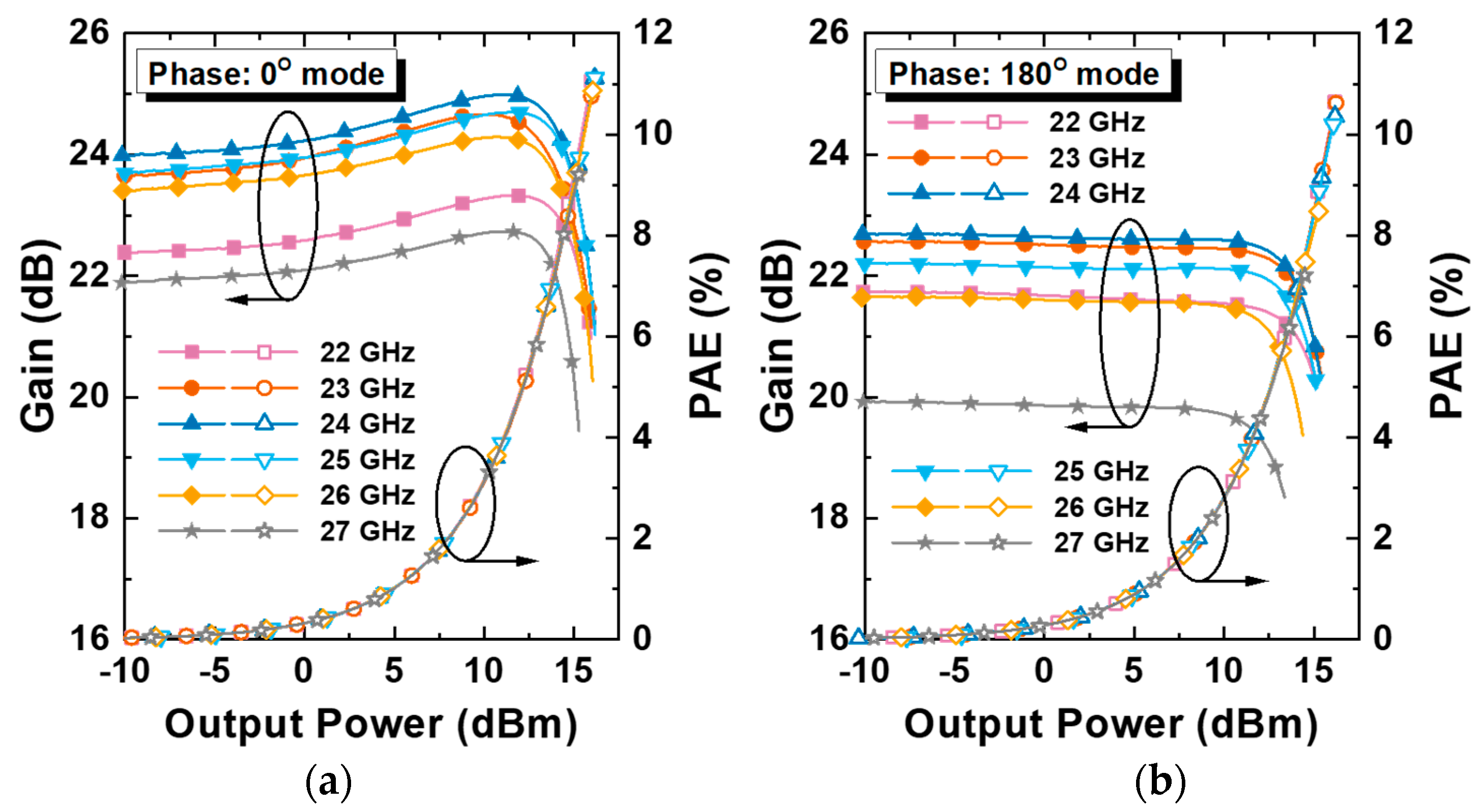
As illustrated in
Figure 9, the power amplifier has a saturation power (
Psat) of 16 dBm or more in the frequency range of 22.0 GHz to 26.0 GHz. However, for the same reason of the parasitic components occurring at the cross-over region of the metal lines, as shown in
Figure 10, the power and PAE were measured to be degraded in the 180°-mode compared to the 0°-mode. The measured P
1dB for the 0°- and 180°-modes were 15.25 dBm and 14.30 dBm, respectively, in the operating frequency of 25.0 GHz.
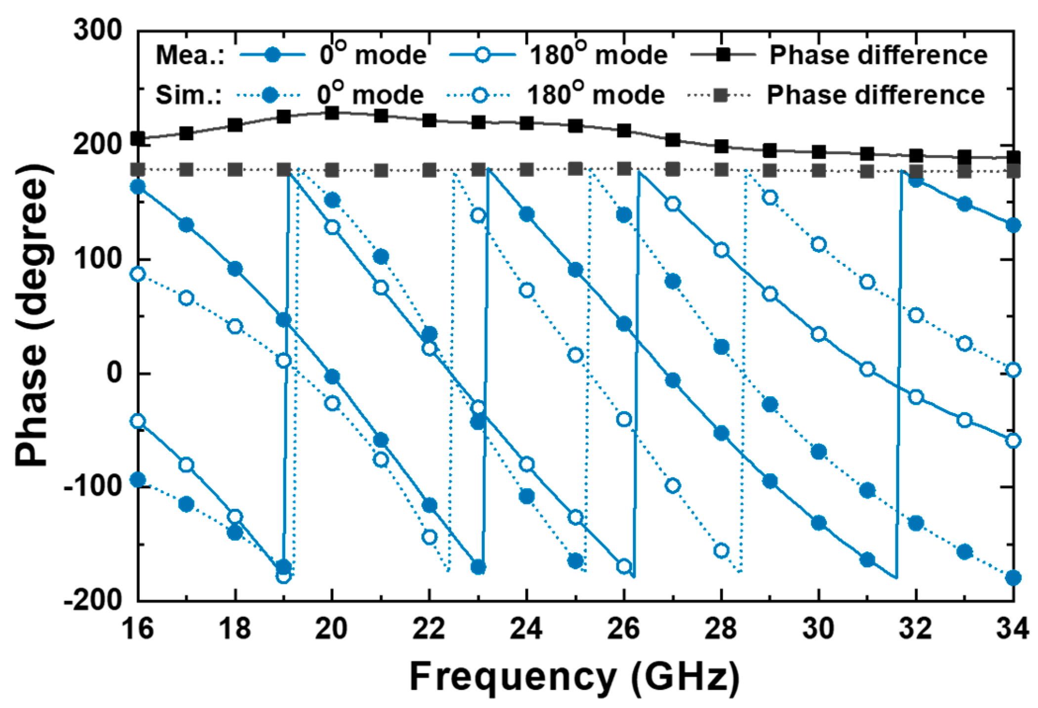
As shown in
Figure 11, the measured phase difference between 0°- and 180°- modes was 217° at the frequency of 25.0 GHz. The cause of the discrepancy of the phase differences of simulated and measured results is expected to be the difference in parasitic capacitance components in the cross-over region of the metal lines circled in
Figure 4.
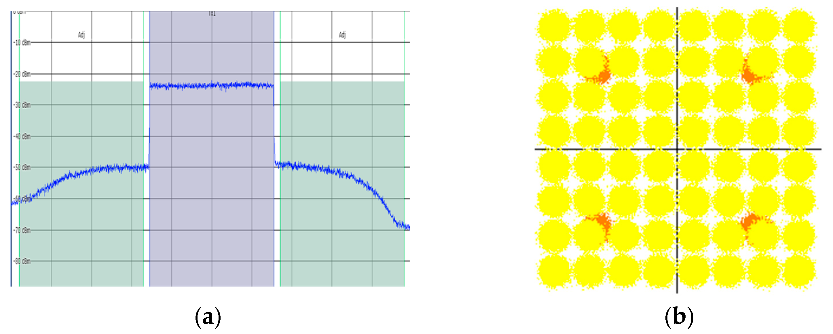
Figure 12 shows the measured output spectrum and constellation for 64-quadrature amplitude modulation (QAM) cyclic prefix (CP)—orthogonal frequency division multiplexing (OFDM) signal with 100 MHz channel bandwidth under error vector magnitude (EVM) −25 dBc condition. When the EVM of −25 dBc was satisfied at 25.0 GHz, the measured output powers were 8.39 dBm and 8.53 dBm for the 0°- and 180°-modes, respectively.
Table 1 shows a comparison with the previous CMOS PAs for 5G applications. The core size of the power amplifier of this study excludes the areas of pads and decoupling capacitors. The PAE was measured somewhat lower due to the power loss in the power transistor due to the low
gm as the power amplifier was fabricated in the slow corner of the LP process. Due to the low
gm of the LP process, the size of the power transistor increased, and the increased transistor required relatively high driving power. Therefore, when
gm was low, power consumption in the driver stages as well as the power stage increased. For this reason, the PAE of the power amplifier designed using a low
gm power transistor deteriorated. However, although the designed power amplifier was fabricated under the slow corner condition of the LP process with a low
gm, as shown in
Figure 1, it can be seen that the designed power amplifier had reasonable output power and gain characteristics compared to those of previous works. In particular, thanks to the four stages structure, the designed power amplifier had the highest gain. Even though the LP CMOS process was used, the linear output power using the modulation signal was similar to that of previous studies. In addition, even though the -shift function was included, the compact size was secured thanks to the application of the proposed structure.


