Article

Grain Orientation and Hardness in the Graded Interlayer of Plasma Sprayed W on CuCrZr

1
Dipartimento di Ingegneria Industriale e Scienze Matematiche, Università Politecnica delle Marche, Via Brecce Bianche 12, 60131 Ancona, Italy
2
Dipartimento di Energia, Divisione di Ingegneria Nucleare, Politecnico di Milano, Piazza Leonardo da Vinci 32, 20133 Milano, Italy
3
Dipartimento di Ingegneria Industriale, Università di Roma “Tor Vergata”, Via del Politecnico 1, 00133 Roma, Italy
4
Dipartimento di Ingegneria Meccanica, Chimica e Dei Materiali, Università di Cagliari, Via Marengo 2, 09123 Cagliari, Italy
5
Faculty of Engineering, eCampus University, Via Isimbardi 10, 22060 Novedrate, Italy
*
Author to whom correspondence should be addressed.
Appl. Sci. 2022, 12(4), 1822; https://doi.org/10.3390/app12041822
Submission received: 10 January 2022 / Revised: 2 February 2022 / Accepted: 8 February 2022 / Published: 10 February 2022

Abstract

:
In this work a W coating was deposited through PS in Ar-H2 atmosphere on a substrate of CuCrZr with an interlayer consisting of gradually changing fractions of Cu and W. The W coating and the interlayer showed good adhesion and no cracks were observed. The hardness of W and Cu along the interlayer was determined by nano-indentation tests and the results showed that a hardness gradient does exist in both the metals. Microstructural examinations suggest that the hardness gradient depends on the texture, which exhibits significant differences along the interlayer: multiplication and movement of dislocations, and localized plasticity under the indenting tip are strongly affected by grain orientation.

1. Introduction

The selection of plasma-facing materials (PFMs) to protect structural components, of divertor and cooling systems, is of fundamental importance for realizing future nuclear fusion reactors. In the International Thermonuclear Experimental Reactor (ITER), PFMs withstand thermal loads ranging from 5 to 20 MW/m2 [1,2] and high particle fluxes. Therefore, they must have a high melting point, excellent thermal conductivity, low activation under neutron irradiation, and very low physical sputtering and tritium retention [3]. Among all the plasma-facing materials (PFMs) considered for building armors, W is the most promising [4,5,6,7,8,9], even though some of its problems are not yet completely solved (e.g., see the review of Linsmeier et al. [10]).
The main drawback of bulk W is its bad machinability, which makes it difficult for it to be used to manufacture complex components, such as the armors protecting the pipes and fittings of cooling systems. To overcome this problem, a possible approach is based on the deposition of W coatings on the cooling system components made of a CuCrZr alloy [11]; however the coefficients of thermal expansion (CTE) of W and Cu alloys are quite different and high residual stresses may arise during cooling to ambient temperature, with consequent crack formation and coating detachment.
Plasma spray (PS) in vacuum or a controlled atmosphere is a highly attractive coating technology owing to the possibility it offers of covering large surfaces, as well as its flexibility and low costs. By using PS in a controlled atmosphere, 5 mm-thick W coatings on CuCrZr substrates were prepared [12,13]; they were able to withstand heat fluxes up to 5 MW/m2 without significant deterioration of integrity or mechanical properties [14]. An interlayer (≈800 µm thick) made of about 20 layers with different compositions was deposited between W and CuCrZr to provide suitable thermo-mechanical compatibility. The interlayer was built by first depositing a layer of pure Ni and then a stratification of layers consisting of graded mixtures of Al-12% Si and Ni-20% Al. The thermo-mechanical performance of the system’s substrate interlayer coating was excellent [15,16]; however, the presence of Ni represents a serious drawback for applications in nuclear fusion reactors owing to its high activation under neutron irradiation. Therefore, a new type of interlayer was investigated without other elements, except for those forming the coating and substrate. This consisted of Cu + W layers with relative amounts of the two metals, which gradually changed from substrate to pure W coating. The same approach was also used by other investigators to deposit W on martensitic steels for structural applications in fusion reactors [17,18].
This article reports some of the results of an extended study carried out through X-ray diffraction (XRD), light microscopy (LM), scanning electron microscopy (SEM), and nano-indentation to characterize the properties of each phase (W and Cu) along the interlayer from substrate to coating. In particular, XRD provides information about the microstructural features averaged over hundreds of W and Cu splats while nano-indentation was performed on each splat. In a previous paper [19], residual stresses were examined, and it was demonstrated that they had different signs in Cu (tensile) and in W (compressive); their maximum value reached in the inner part of the interlayer, where the relative amounts of the two deposited metals were similar. Here, our attention is focused on the trend of hardness in both metals along the interlayer.

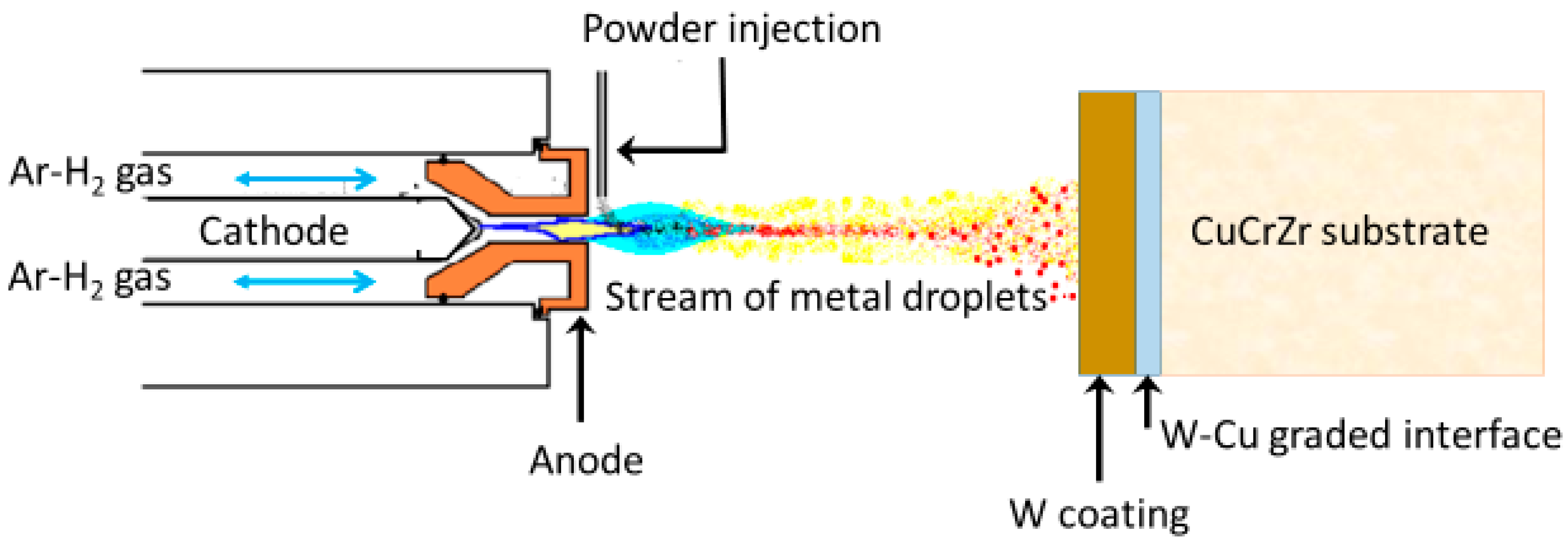
2. Materials and Methods

The examined sample was a cylinder with a diameter of 30 mm and a height of 10.6 mm; a cross-section is shown in Figure 1.
The CuCrZr alloy forming the substrate had the following nominal composition: Cr 0.65, Zr 0.05, Cu to balance (wt%).
Deposition was performed through PS technique in controlled atmosphere (a mix of Ar-H2 gases) at a pressure of 600 mbar. Figure 2 shows a schematic view of the PS apparatus.
The main deposition parameters were selected on the basis of some preliminary tests: torch speed of 800 mm/s, torch–surface distance of 180 mm, substrate temperature of 180 ± 5 °C. The thickness of W coating was ~1.6 mm while that of the interlayer was ~1.2 mm. The interlayer was made of a mixture of pure Cu and W and was obtained by depositing eight layers with nearly the same thickness (150 μm) and different composition by adjusting the powder feed rates.
The composition of the layers forming the interlayer gradually changed with increasing amounts of W moving from the substrate to the coating. The volume fractions of W and Cu in each deposited layer are reported in Table 1.
Observations using light microscopy (LM) (Union Optical Co., Ltd., Tokyo, Japan) and scanning electron microscopy (SEM) Hitachi SU70 (Hitachi, Tokyo, Japan) were carried out on the cross-section of the sample after surface polishing by means of increasingly fine grinding papers. To characterize the interlayer structure, SEM observations were also carried out on the fracture surface of the samples broken in three-point bending tests.
We carried out XRD (Philips, Eindhoven, The Netherlands) measurements on the CuCrZr substrate, interlayer, and W coating by illuminating the cross-section and shifting the sample with increasing steps of 250 µm. A schematic view of the experimental set-up is shown in [19]. In this way, five zones of the interlayer were examined (1–5, moving from substrate to coating). The rectangular X-ray spot had constant length of 15 mm and width changing with 2Θ angle. At the maximum angle of analysis (2Θ = 75°), the spot width was about 250 µm. Since the step of analysis and the width of X-ray spot had substantially the same value, the whole interlayer was examined without overlapping zones. Given that the width of the X-ray spot was larger than each deposition step (150 μm), the five zones did not correspond to the single deposition steps.
The Cu- radiation (λ = 0.15408 nm) was used to collect XRD patterns in the 2Θ angular range 35–150° with 2Θ steps of 0.05° and counting time of 5 s per step. The peaks at 2Θ angles > 75° demonstrated negligible intensity and were comparable to the background values; thus, they were not considered in the analysis.
To evaluate possible textures in the examined zones, the relative intensities of the XRD reflections were compared to those reported in the JCPDS-ICDD database (W-File 4-806, Cu-File 4-0836) [20] referring to metals with random grain orientation.
To determine the dislocation density, high precision peak profiles of the most intense reflections were recorded with 2Θ steps of 0.005° and counting time of 20 s per step.
Hardness (H) was been measured through the nano-indentation technique by using a Hysitron© Inc. triboscope nanoindenter Ubi-1® (Minneapolis, MN, USA). Uniaxial compression was performed by using a three-sided pyramidal Berkovich tip with edge aperture angle of 65.35° and tip curvature radius of 120 nm. The nanoindentation measurements were analyzed according to the Oliver and Pharr method [21,22,23]. Thus, H was determined by full cycles of load–unloading print. Accordingly, the unloading curve was fitted with the power-law relationship P = B (hhf) k, where P is the tip load, h the displacement, hf the extent of displacement after unloading, and B and k are the fitting parameters. The penetration contact depth, hc, can be estimated by hc = hMaxη(PMax/S), where hMax is the maximum indenter penetration depth at the peak load, PMax, η is a tip-dependent constant that for a Berkovich tip is 0.75, and S the material stiffness. Calibration was carried out on fused quartz (Er = 72 GPa) according to the specifications described by Cabibbo et al. [24]. In this regard, a trapezoidal load function, consisting of the same load and unload rates to the peak load PMax = 8 mN at a speed of 5 s, as well as a dwelling peak load of 2 s, was used. In particular, in the nano-indentation tests, load (P) and penetration depth (h) were measured step-by-step during the loading–unloading cycle.
Nano-indentation measurements were spaced 50 μm apart and spanned from W to CuCrZr. Four different measurement runs were carried out to obtain a statistically sound series of data. In this respect, the obtained hardness values at each characteristic zone, i.e., from CuCrZr substrate throughout the W full deposition zone, resulted from the average of four individual measurements carried out with a mean distance of 250 μm between each zone. Hence, a minimum of 80 measurements were carried out on full W deposition zones and CuCrZr alloy where no W traces were present; and a minimum of 16 measurements at each characteristic zone of the Cu–W interlayer were also carried out, that is, at a 50 μm-wide pace, from CuCrZr substrate to full W deposition, as shown in Table 1.

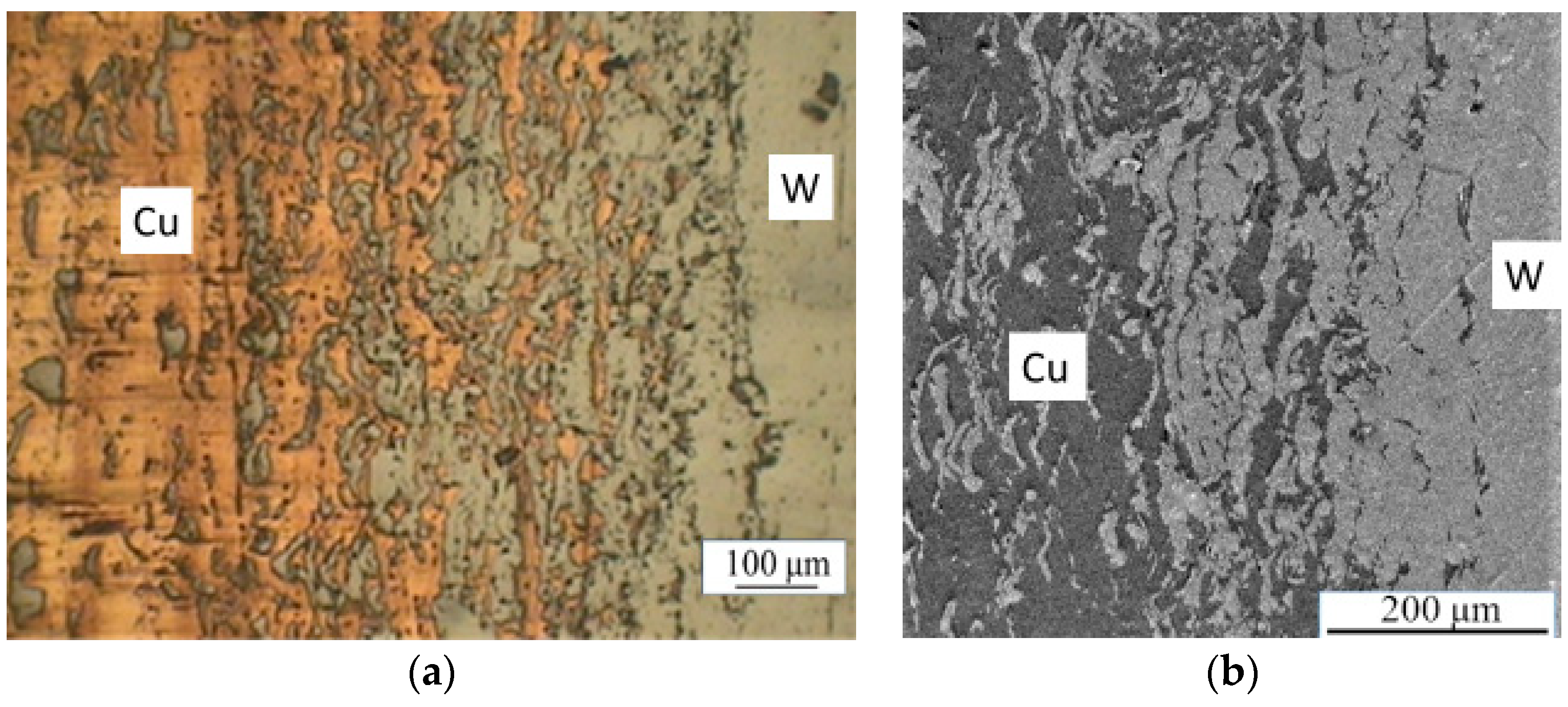
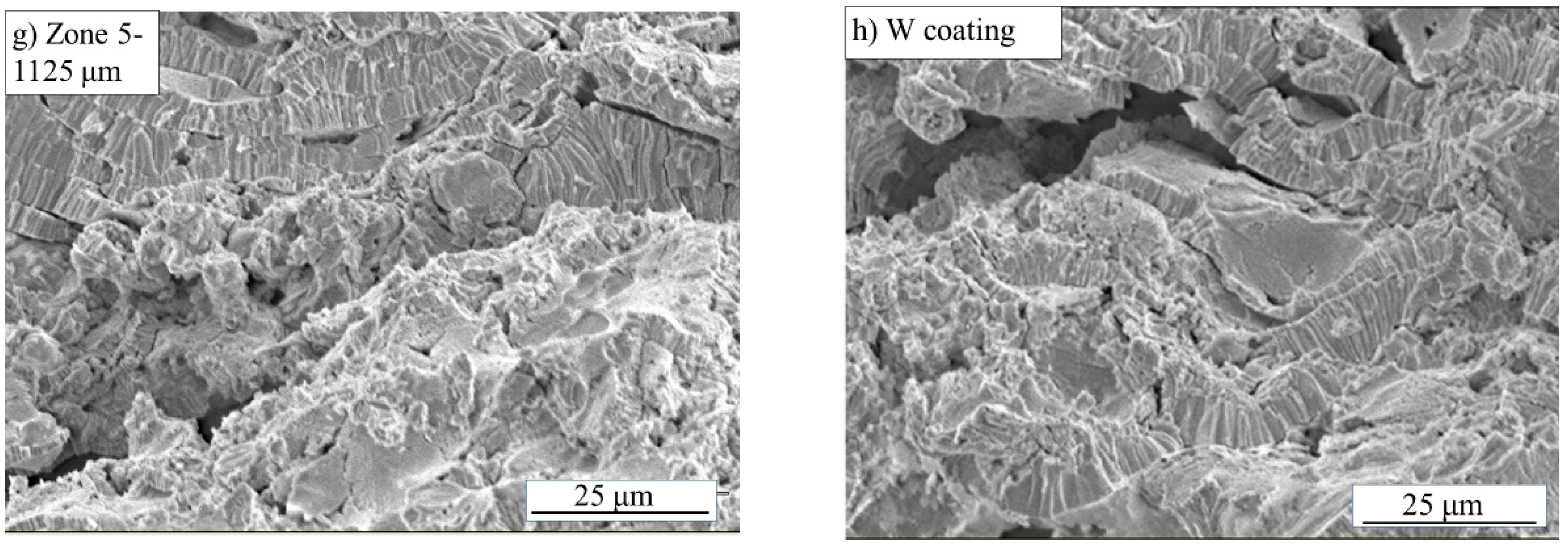
3. Results and Discussion

The micrographs at different magnifications in Figure 3a,b show the interlayer where Cu and W splats exhibit a complex and irregular morphology. The W coating and the interlayer showed good adhesion and no cracks were observed.
The fracture surface of the samples broken in the three-point bending tests were examined through SEM observations to investigate the specific microstructural features of both metals in the interlayer.
Figure 4 shows representative micrographs recorded at different distances from the substrate.
The zones from 1 to 5 indicated in each photo correspond to those of the XRD measurements. In all the examined zones, Cu and W can be identified because they exhibit quite different fracture modes. The Cu areas show large amounts of dimples, revealing a typical ductile fracture mode. By contrast, W always exhibits a brittle inter-crystalline mode of fracture. For example, the specific features can be seen in the areas indicated by markers in Figure 4c. Some unmolten particles, indicated by red arrows in the first micrograph of Figure 4, can be observed in different positions of the interlayer and W coating.
It was demonstrated that W has a complex and fine layered structure arising from the impact of metal droplets on its surface. Each layer consists of many columnar grains whose thickness dT (see Figure 5) is usually that of the layer, while the length substantially corresponds to the size of the original impacting droplet. The morphology of W grains is substantially the same across the interlayer and coating: the average thickness dT is ~ 6 μm, while the grain width dW ranges from 0.5 to 1 μm. In fact, the grains exhibit an irregular lamella-like shape, with one dimension much larger than the other two. The W layers are about parallel to the deposition surface in zones 1 and 2, where Cu is the prevalent element, whereas in zone 5, they display different orientations.
The XRD patterns collected in the different zones across the interface are shown in Figure 6.
The examined zones of the interlayer correspond to successive shifts (250 μm) of the sample under the X-ray beam, starting from the substrate to the coating. To evaluate possible preferred grain orientations, the relative intensities of W and Cu peaks in each XRD pattern displayed in Figure 6 were determined and compared to data taken from the JCPDS X-ray database (Cu-4-836 and W-4-806 files), referring to the metals with randomly oriented grains. The relative intensities of the diffraction peaks after normalization to the most intense reflection (I = 100) are reported in Table 2. For each zone, the central position of the X-ray spot is indicated.
The relative intensities of the XRD reflections reported in the JCPDS X-ray database [20] correspond to those of the material with randomly oriented grains. If the examined material has a texture, the intensities diverge from the reference values: the greater the difference, the stronger the texture. On this basis, an index was used to quantitatively describe the strength of each texture component. This index takes into account the ratio between the intensity of a given peak and that of the highest peak in the examined and reference materials. In the case of Cu, the index of the <100> texture component is (I200/I111)/(I200/I111)R while that of the <110> texture component is (I220/I111)/(I220/I111)R. The subscript R indicates a random orientation. For W (I200/I110)/(I200/I110)R and (I211/I110)/(I211/I110)R describe the <100> and <211> texture components, respectively. Of course, if the grains have a full random grain orientation, the index is 1 for each texture component.
Figure 7 shows the texture index of Cu (a) and W (b) in the examined zones calculated from the data in Table 2.
The CuCrZr substrate has a principal <110> texture and a secondary <100> cubic component. In the first deposited layers of Cu (zones 1 and 2), these texture components become even stronger; subsequently, starting from a distance of ~500 μm, they progressively weaken, and finally the Cu grains take on an almost random orientation near the coating (zones 4 and 5).
The XRD patterns of W collected from zones 1 and 2 exhibit only a very weak (110) peak with intensity comparable to the background; thus, they are not suitable for describing a possible texture. In the zones 4 and 5 and the coating, the relative intensities do not significantly diverge from those corresponding to the random grain orientation; only weak <100> and <211> texture components were observed there.
The dislocation density of Cu and W in the different zones was determined from the analysis of the XRD peak profiles, namely from their half-height line widths. The Cu peaks recorded in different positions of the interlayer were shown to be quite similar, whereas those of W exhibited different broadening, depending on the specific position.
For example, Figure 8 shows the Cu (220) and W (211) peaks collected in different positions in the interlayer. To better compare the broadening of the peaks, they were suitably shifted to occupy the same central position. After correction from instrumental contribution, the total broadening βT of each peak is basically the sum of two terms, namely the size of coherently diffracting domains (βD) and of the micro-strains (βε):
β T = β D + β ε = K λ D cos Θ + 2 ε tan Θ
where D is the domain size (in this case grain size), ε is the average micro-strain, Θ is the Bragg angle, λ is the wavelength, and K is a constant (=0.89).
As shown in Figure 3 and Figure 4, the value of D in both the metals (W and Cu) is of the order of some microns. Thus, the contribution to peak broadening due to the size of coherently diffracting domains (βD) can be neglected and βTβε. Therefore, the average micro-strain ε was directly determined from βT and the dislocation density ζ calculated by means of the Williamson–Smallman equation [25]:
ζ = Ξ ε 2 k 0 b 2
where Ξ = 16 is a constant, b is the modulus of the Burgers vector (0.2556 nm for Cu, 0.2735 nm for W), and k0 ≅ 1 is a factor depending on dislocation interaction.
The dislocation density of Cu is similar in all the examined zones and its value is ≈3 × 10¹³ m−2, whereas that of W slightly decreases, moving from zone 3 (6 × 10¹⁴ m−2) to zone 5 (2 × 10¹⁴ m−2).
Figure 9 shows the typical load-displacement nano-indentation curves measured inside Cu (a) and W (b) splats in different positions of the interlayer.
Nano-indentations were performed in the interlayer region along line paths from the substrate to the W coating. At the interlayer, it was shown that through the applied load of PMax = 8000 μN, the indentation tip reached a penetration depth ranging 300–380 nm in Cu. On the other hand, the penetration depth was halved (to approximately 200 nm) in W.
Figure 10 displays a plot of the hardness H of Cu and W measured across the interlayer from the CuCrZr substrate to the W coating. The deposited Cu exhibits a near-constant hardness (H = 2.2 ± 0.2 GPa) up to a distance of 800 μm from the substrate; the hardness then starts to rise continuously with a parabolic-like trend until it reaches a value of 3.9 ± 0.2 GPa near the W coating. Correspondingly, the hardness trend of the deposited W is significantly different. In this case, the hardness continuously increases from 3.8 ± 0.3 GPa in the vicinity of the CuCrZr substrate up to 9.9 ± 0.1 GPa at the opposite edge of the W–Cu deposition interlayer zone.
A critical aspect of these tests was represented the by nano-indentations taken at the boundary between Cu and W splats; these measures gave rise to false results that needed to be discarded. Since microscopic inspection does not always guarantee a reliable identification of these occurrences, the curves corresponding to tests carried out at Cu–W boundaries were identified from the abrupt slope change in the loading stage, which is not present in the curves obtained by indenting homogeneous areas (Cu or W). In fact, the slope change occurs when one tip, which at the beginning of indentation penetrates into one of the two metals, starts to interact with the other. A more detailed explanation of the method is reported in [19].
The interlayer consists of Cu and W splats with irregular shapes (Figure 3) and, as shown for residual stresses in a previous paper [19], the properties of W and Cu vary along the interlayer. The results presented in this article evidence how the hardness of the two phases changes with the distance from the substrate.
In fusion reactors, during service, W armors are irradiated by energetic neutrons, leading to the formation and accumulation of lattice defects and to transmutation with products such as Re, Os, Ta, H, and He [26]. Moreover, W is also exposed to direct bombardment by H and He from plasma [27]. An extensive description of the physical phenomena occurring in W during H and He interactions is given in [28]; here, it is noteworthy that at high temperatures, H and He atoms have high mobility for interstitial diffusion towards defects, resulting in increasing hardness, which is to the detriment of ductility. This is a serious concern for the long-term structural integrity of armors; thus, the presence of a hardness gradient in the interlayer before irradiation must be well understood. Therefore, to find the causes of the specific trends displayed in Figure 10, the grain size, dislocation density and texture of both phases were considered the main factors that play a role in the plastic deformation of pure metals.
The results of the microstructural examinations clearly indicate that variations in grain size or dislocation density could not have been responsible for the hardness trend of W: the average thickness dT and width dW of W lamella-shaped grains is substantially the same in the whole interlayer (Figure 4), while the dislocation density slightly decreases, moving towards the coating. Analogous considerations can be made for Cu. Thus, our attention was focused on the texture of both phases, which shows significant changes depending on the specific position in the interlayer.
The characteristics of the deposited metal are critically affected by the interaction with the substrate; however, the specific mechanisms of nucleation and growth depend on the technology used for depositing the metal and process parameters (for an example, see [29,30,31]). The topic is too complex to be explored exhaustively owing to the large variety of deposition techniques and the many parameters involved in each of them. Recently, He et al. [31] described the growth of yttria-stabilized zirconia (YSZ) coatings prepared by means of plasma spray-physical vapor deposition (PS-PVD) as a three-stage process, as follows: (i) the formation of many randomly orientated grains of small size, (ii) the development of these small grains into elongated grains without preferred crystallographic orientation, and (iii) the reduction of the number of columnar grains and the coating growth along preferred orientations. The study clearly highlights the complexity of phenomena occurring in PS deposition; however, the model cannot be directly adopted to explain the textures observed in the experiments reported in this article because a large part of powder feedstock in PS-PVD is evaporated whereas in PS the metal is deposited in the liquid state (droplets of Cu or W). As a consequence, textures originated from preferential grain growth in PS-PVD, and from repeated nucleation and growth in PS.
As shown by Figure 7a, the substrate of CuCrZr alloy exhibits a strong <110> texture with a secondary <100> component. Thus, in the first deposited layer (90% Cu and 10% W), the droplets of liquid Cu impact directly on the substrate and in large part solidify with the same orientation of the CuCrZr grains. This phenomenon also occurs in the successive layers up to a distance of ~450 μm from the substrate; it then progressively weakens as the amount of W in the interlayer increases and completely disappears near the W coating, where Cu grains have a nearly random orientation.
The case of W is different because the droplets impacting on the Cu phase give rise to the incipient melting of Cu due to its lower melting point [32]. Owing to the occurrence of this phenomenon, the orientation of the new W grains forming after solidification is scarcely affected by that of grains already present in the surface of deposition. Therefore, as was made evident by comparing the specific texture index values, the [211] and [100] texture components of W are weaker than those of Cu.
Recent results published by Yu et al. [33] showed that the nano-indentation behavior of pure W is strongly dependent on grain orientation because this affects nucleation and the movement of dislocations under the indenting tip. Through high-resolution electron backscatter diffraction (HR-EBSD) around nano-indents, these investigators were able to reveal pile-up for Burgers vectors inclined to the surface at an angle greater than ~20°, whereas dislocation transport channels without pile-up were observed for Burgers vectors near-parallel to the sample surface. The same effect was also observed in other materials, such as WC-Co [34], TiAl [35], Cu [36,37,38], Ni, and Fe [38]. In fact, the orientation of the indented grain can determine the onset of either hardening or softening mechanisms.
On these grounds, the increasing hardness observed in W zones of the interlayer moving from substrate towards the coating can be related to the progressive evolution of the texture to the strengthening of the [100] component. Grains with this orientation present the localization of plasticity and pile-up around the indent [33] with a consequent increase in the measured hardness.
Analogous considerations can be made for Cu, where the mechanical performances of [111] oriented grains are superior to those of any other grain [36]. Near the substrate and in the middle of the interlayer, the strongest texture components of Cu are [100] and [110]: the prevalent orientations of the grains are those corresponding to the lowest mechanical strength. The hardness increase observed near the coating corresponds to the texture evolution towards random grain distribution. This change involves a larger fraction of grains having a (111) orientation with higher resistance to indentation.
We hope that the main result of this work, namely the presence of a hardness gradient along the interlayer and its dependence on grain orientation, will stimulate further investigations in the fusion community for predicting the behavior of W armors during service in a tokamak, with particular attention to the interaction of H and He with lattice defects of W, that is not yet completely understood, and contradictory results have been published [38,39,40].

4. Conclusions

W coating was deposited by means of PS in an Ar-H2 atmosphere on a substrate of CuCrZr, with an interlayer consisting of gradually changing fractions of Cu and W. The W coating and the interlayer showed good adhesion and no cracks were observed. The work investigated the hardness of the two metals along the interlayer through nano-indentation tests in correlation with their microstructural characteristics. The results can be summarized as follows.
(i)
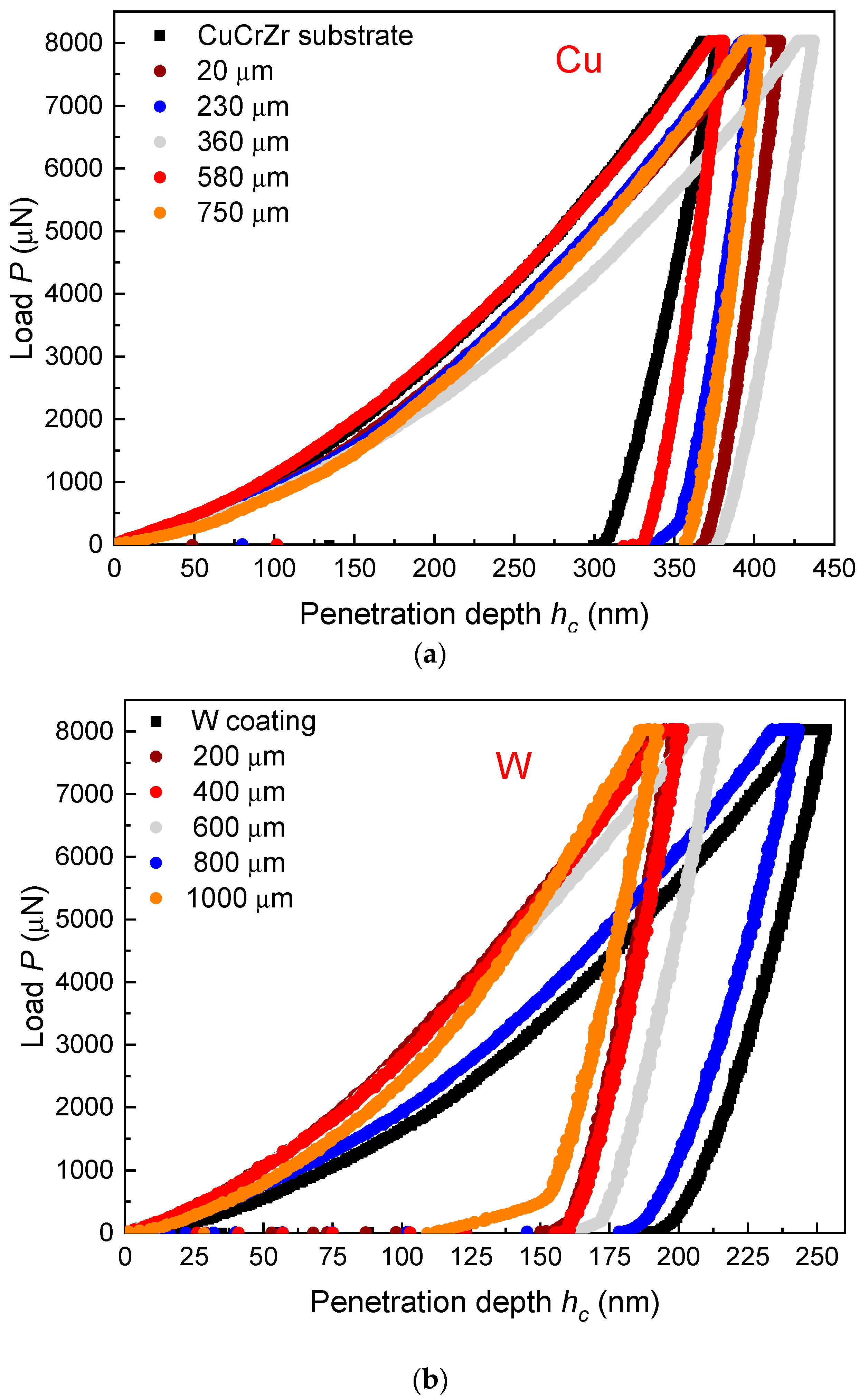
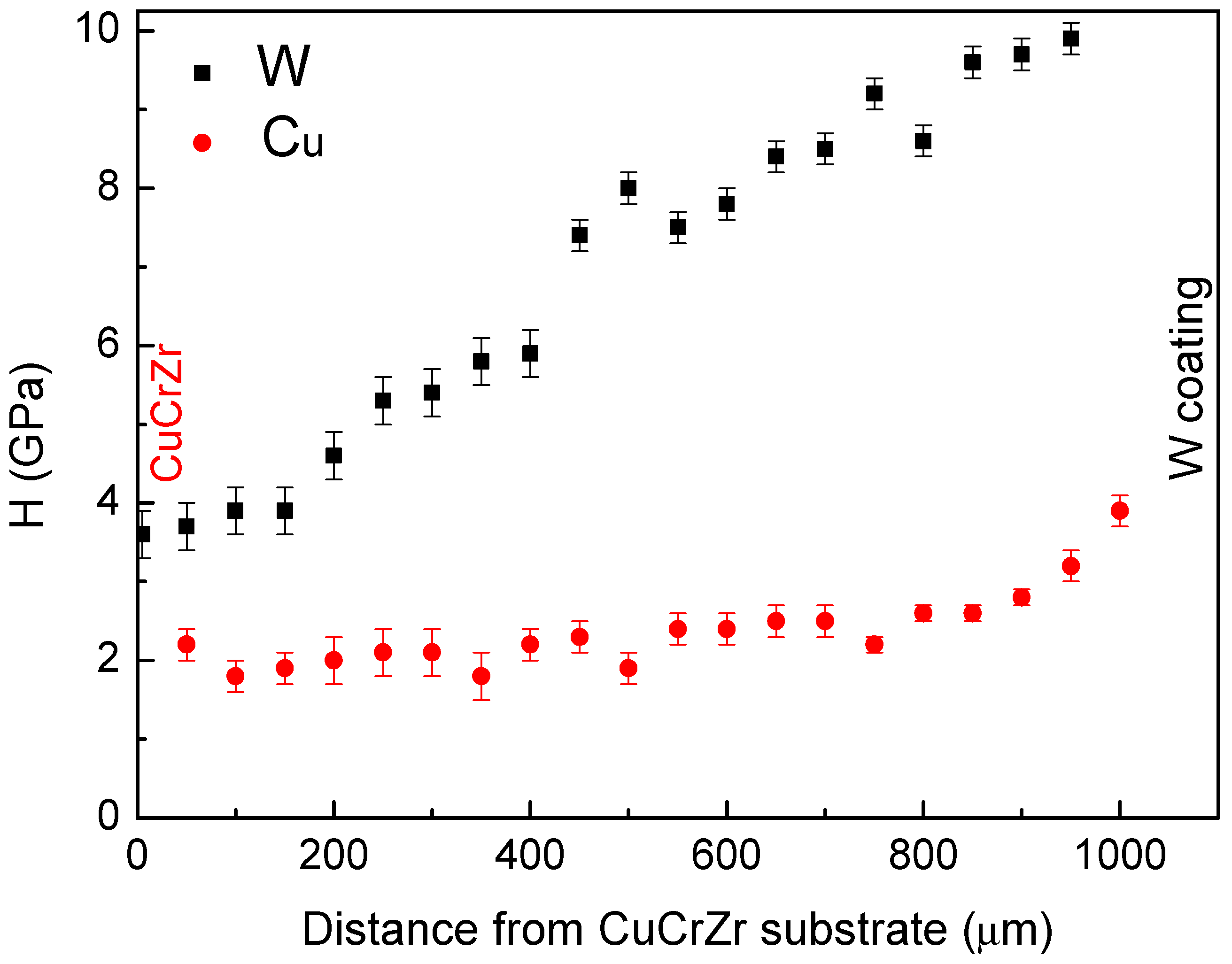
Both metals exhibit a hardness gradient in the interlayer: hardness of Cu is nearly constant (2.2 ± 0.2 GPa) up to a distance of ~800 μm from the substrate; it then increases until it reaches a value of 3.9 ± 0.2 GPa near the coating, while that of W continuously increases from 3.8 ± 0.3 GPa near the substrate up to 9.9 ± 0.1 GPa on the opposite side.
(ii)
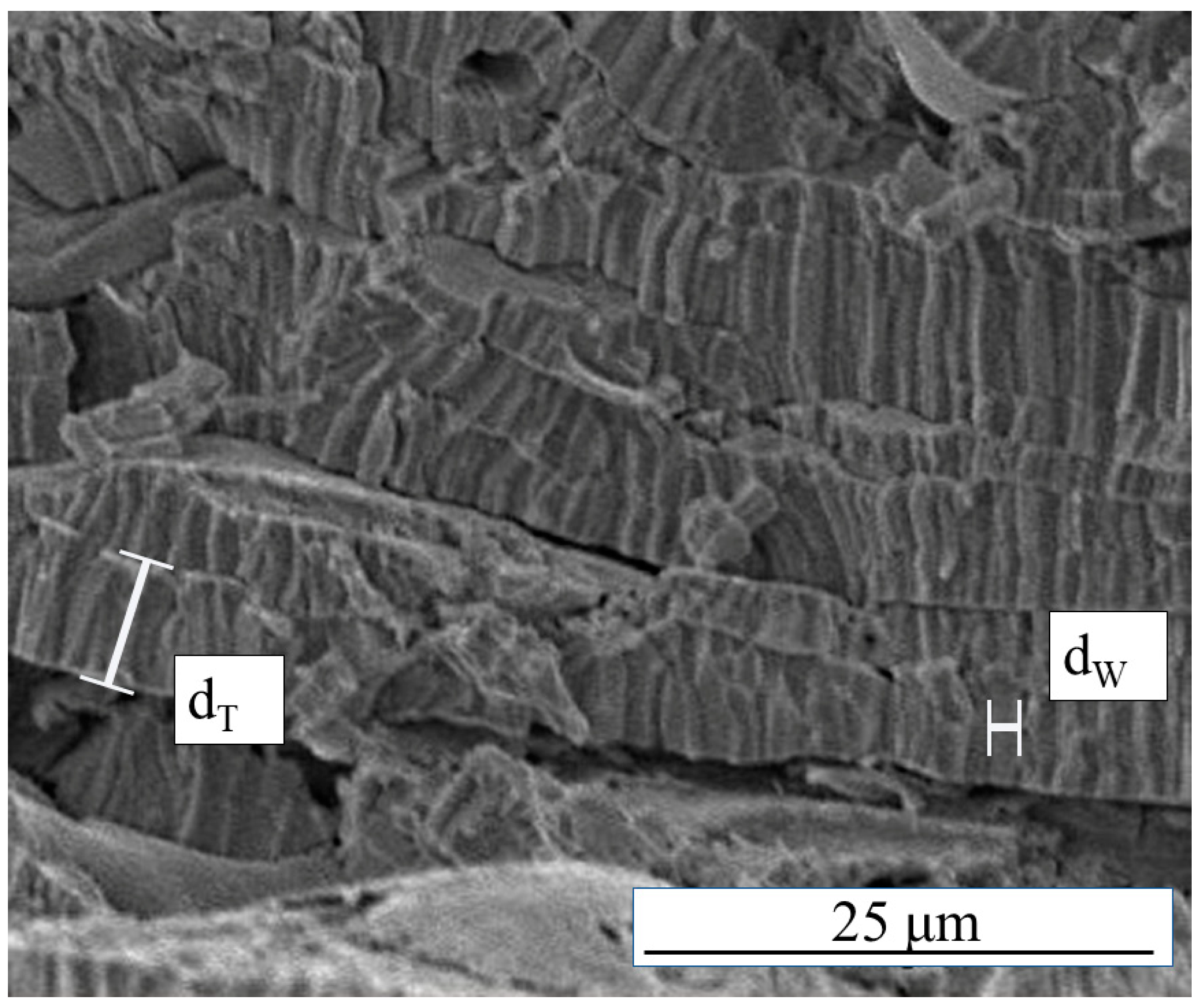
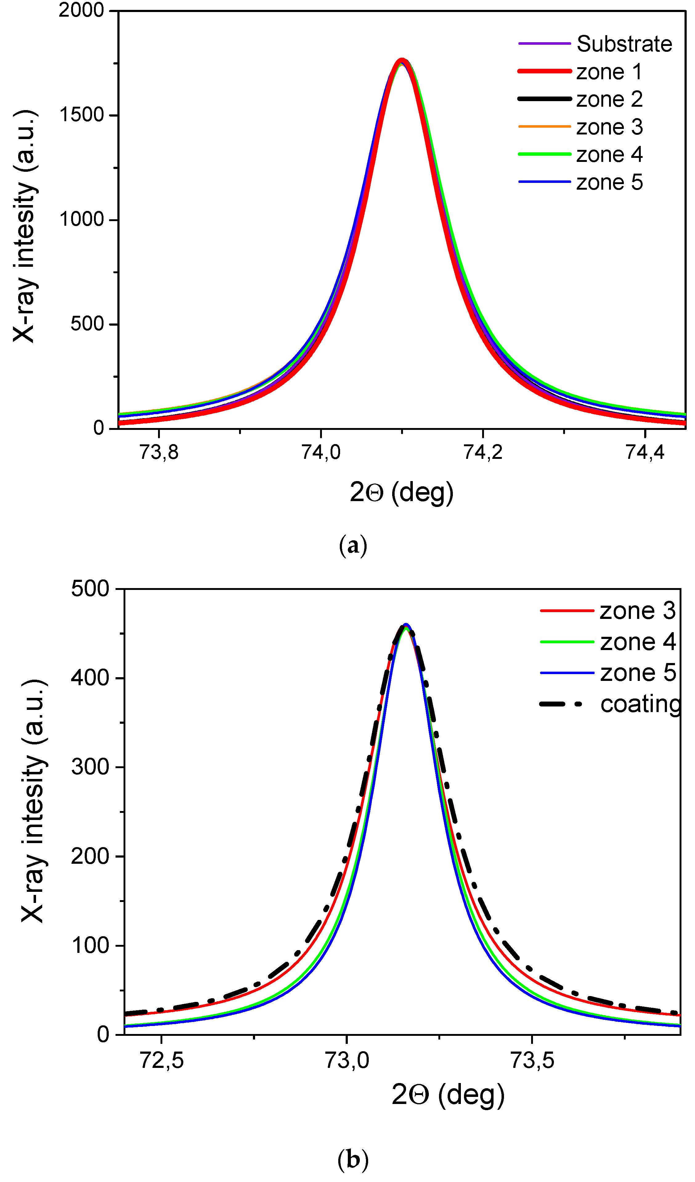
The grain morphology and size of W and Cu do not change substantially along the interlayer; the dislocation density is constant in Cu, while it slightly decreases in W near the coating.
(iii)
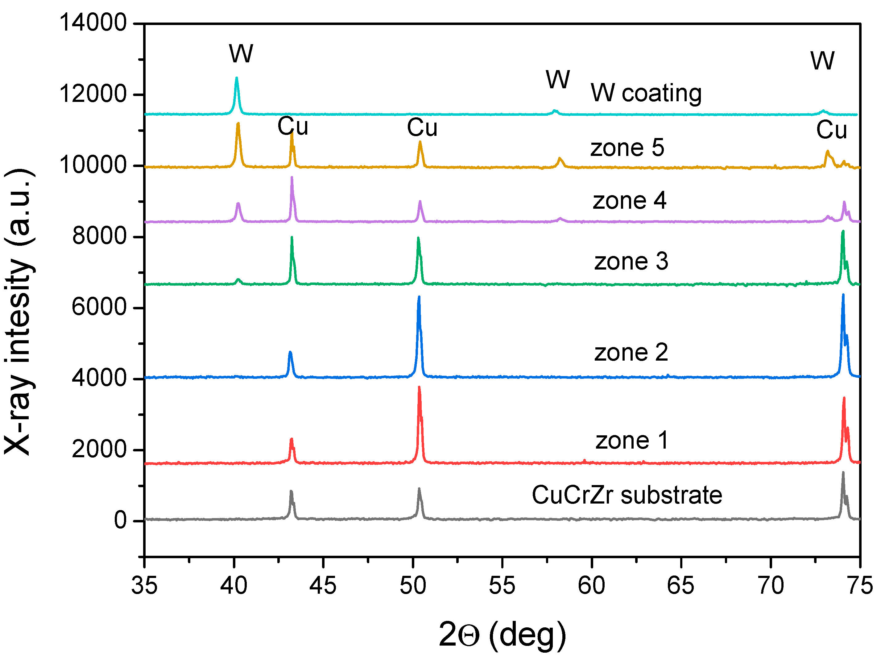
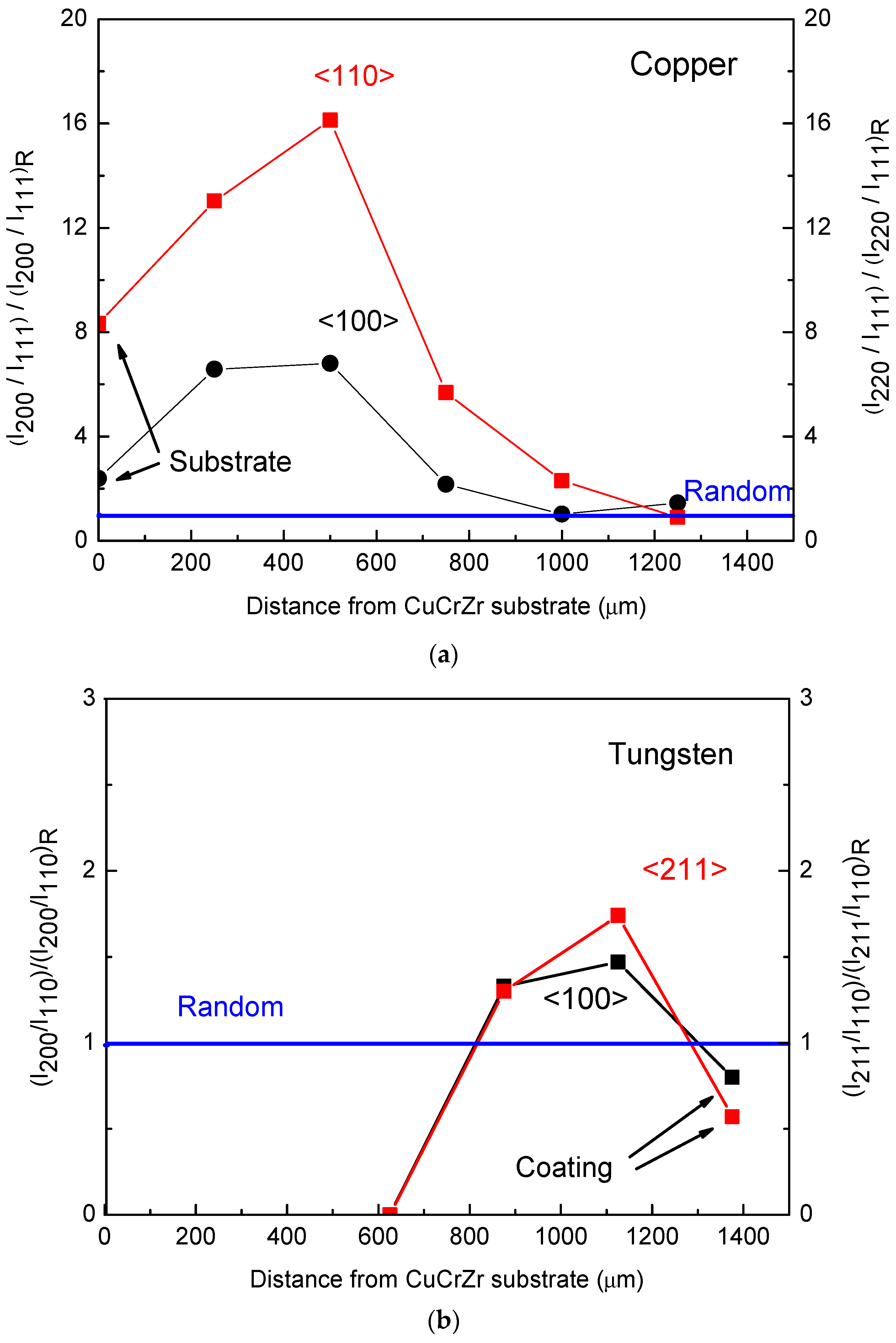
The texture of both W and Cu exhibits significant differences, depending on the specific position in the interlayer.
(iv)
The preferred orientation of crystalline grains, which is the result of a process of repeated nucleation and growth occurring when droplets impact the surface and solidify, is the key factor explaining the observed hardness gradients. The multiplication and movement of dislocations, and localized plasticity under the indenting tip, are strongly affected by grain orientation.

Author Contributions

Conceptualization, E.P., R.M. and M.C.; methodology, E.P., A.F., A.V., C.P. and M.R.; formal analysis, R.M., M.R. and A.V.; supervision, R.M. and M.C.; draft paper preparation, E.P. and R.M.; final paper preparation, all authors. All authors have read and agreed to the published version of the manuscript.

Funding

This research received no external funding.

Institutional Review Board Statement

Not applicable.

Informed Consent Statement

Not applicable.

Data Availability Statement

The data presented in this study are available on request from the corresponding author.

Acknowledgments

The authors are grateful to Piero Plini of Department of Industrial Engineering—University of Rome “Tor Vergata” for the assistance in sample preparation.

Conflicts of Interest

The authors declare no conflict of interest.

References

  1. Linke, J.M.; Hirai, T.; Rödig, M.; Singheiser, L.A. Performance of Plasma-Facing Materials Under Intense Thermal Loads in Tokamaks and Stellarators. Fusion Sci. Technol. 2017, 46, 142–151. [Google Scholar] [CrossRef]
  2. Linsmeier, C.; Unterberg, B.; Coenen, J.W.; Doerner, R.P.; Greuner, H.; Kreter, A.; Linke, J.; Maier, H. Material testing facilities and programs for plasma facing component testing. Nucl. Fusion 2017, 57, 092012. [Google Scholar] [CrossRef] [Green Version]
  3. Linke, J.; Du, J.; Loewenhoff, T.; Pintsuk, G.; Spilker, B.; Steudel, I.; Wirtz, M. Challenges for plasma-facing components in nuclear fusion. Matter Radiat. Extrem. 2019, 4, 056201. [Google Scholar] [CrossRef] [Green Version]
  4. Philipps, V. Tungsten as material for plasma-facing components in fusion devices. J. Nucl. Mater. 2011, 415, S2–S9. [Google Scholar] [CrossRef]
  5. Hirai, T.; Panayotis, S.; Barabash, V.; Amzallag, C.; Escourbiac, F.; Durocher, A.; Merola, M.; Linke, J.; Loewenhoff, T.; Pintsuk, G.; et al. Use of tungsten material for the ITER divertor. Nucl. Mater. Energy 2016, 9, 616–622. [Google Scholar] [CrossRef] [Green Version]
  6. Wirtz, M.; Linke, J.; Loewenhoff, T.; Pintsuk, G.; Uytdenhouwen, I. Thermal shock tests to qualify different tungsten grades as plasma facing material. Phys. Scr. 2016, T167, 014015. [Google Scholar] [CrossRef]
  7. Montanari, R.; Pakhomova, E.; Pizzoferrato, R.; Richetta, M.; Varone, A. Laser pulse effects on plasma sprayed and bulk tungsten. Metals 2017, 7, 454. [Google Scholar] [CrossRef] [Green Version]
  8. Gaudio, P.; Montanari, R.; Pakhomova, E.; Richetta, M.; Varone, A. W-1% La2O3 Submitted to a Single Laser Pulse: Effect of Particles on Heat Transfer and Surface Morphology. Metals 2018, 8, 389. [Google Scholar] [CrossRef] [Green Version]
  9. Montanari, R.; Pakhomova, E.; Rossi, R.; Richetta, M.; Varone, A. Surface Morphological Features of Molybdenum Irradiated by a Single Laser Pulse. Coatings 2020, 10, 67. [Google Scholar] [CrossRef] [Green Version]
  10. Linsmeier, C.; Rieth, M.; Aktaa, J.; Chikada, T.; Hoffmann, A.; Hoffmann, J.; Houben, A.; Kurishita, H.; Jin, X.; Li, M.; et al. Development of advanced high heat flux and plasma-facing materials. Nucl. Fusion 2017, 57, 092007. [Google Scholar] [CrossRef]
  11. Lipa, M.; Durocher, A.; Tivey, R.; Huber, T.; Schedler, B.; Weigert, J. The use of copper alloy CuCrZr as a structural material for actively cooled plasma facing and in vessel components. Fusion Eng. Des. 2005, 75–79, 469–476. [Google Scholar] [CrossRef]
  12. Riccardi, B.; Montanari, R.; Moreschi, L.F.; Sili, A.; Storai, S. Mechanical characterization of fusion materials by indentation test. Fusion Eng. Des. 2001, 58–59, 755–759. [Google Scholar] [CrossRef]
  13. Montanari, R.; Riccardi, B.; Volterri, R.; Bertamini, L. Characterisation of plasma sprayed W-coatings on a CuCrZr alloy for nuclear fusion reactor applications. Mater. Lett. 2002, 52, 100–105. [Google Scholar] [CrossRef]
  14. Riccardi, B.; Montanari, R.; Casadei, M.; Costanza, G.; Filacchioni, G.; Moriani, A. Optimisation and characterisation of tungsten thick coatings on copper based alloy substrates. J. Nucl. Mater. 2006, 352, 29–35. [Google Scholar] [CrossRef] [Green Version]
  15. Ciambella, L.; Maddaluno, G.; Montanari, R.; Pakhomova, E. Residual stresses in tungsten deposited by plasma; spraying: Effect of substrate and processing methods. Metall. Ital. 2015, 107, 31–39. [Google Scholar]
  16. Fava, A.; Pakhomova, E.; Varone, A. Study of residual stresses through X-ray diffraction of a W/Cu interlayer deposited by plasma spraying. Metall. Ital. 2020, 112, 16–25. [Google Scholar]
  17. Vaßen, R.; Rauwald, K.-H.; Guillona, O.; Aktaa, J.; Weber, T.; Back, H.C.; Qu, D.; Gibmeier, J. Vacuum plasma spraying of functionally graded tungsten/EUROFER97 coatings for fusion applications. Fusion Eng. Des. 2018, 133, 148–156. [Google Scholar] [CrossRef]
  18. Emmerich, T.; Qu, D.; Vaßen, R.; Aktaa, J. Development of W-coating with functionally graded W/EUROFER-layers for protection of First-Wall materials. Fusion Eng. Des. 2018, 128, 58–67. [Google Scholar] [CrossRef] [Green Version]
  19. Cabibbo, M.; Fava, A.; Montanari, R.; Pakhomova, E.; Paoletti, C.; Richetta, M.; Varone, A. Residual stresses in the graded interlayer between W and CuCrZr alloy. J. Mater. Sci. 2022, 57, 285–298. [Google Scholar] [CrossRef]
  20. JCPDS-International Centre for Diffraction Data, Newtown Square, PA 19073, USA. Available online: https://www.icdd.com/pdfsearch/ (accessed on 5 January 2022).
  21. Pharr, G.M.; Oliver, W.C.; Brotzen, F.R. On the generality of the relationship among contact stiffness, contact area, and elastic modulus during indentation. J. Mater. Res. 1992, 7, 613–617. [Google Scholar] [CrossRef]
  22. Oliver, W.C.; Pharr, G.M. An improved technique for determining hardness and elastic modulus using load and displacement sensing indentation experiments. J. Mater. Res. 1992, 7, 1564–1583. [Google Scholar] [CrossRef]
  23. Pharr, G.M. Measurement of mechanical properties by ultra-low load indentation. Mater. Sci. Eng. A 1998, 253, 151–159. [Google Scholar] [CrossRef]
  24. Cabibbo, M.; Ricci, P.; Cecchini, R.; Rymuza, Z.; Sullivan, J.; Dub, S.; Cohen, S. An international round-robin calibration protocol for nanoindentation measurements. Micron 2012, 43, 215–222. [Google Scholar] [CrossRef] [PubMed]
  25. Williamson, G.K.; Smallman, R.A. Dislocation densities in some annealed and cold-worked metals from measurements on the X-ray debye-scherrer spectrum. Phil. Mag. 1956, 1, 34–46. [Google Scholar] [CrossRef]
  26. Gilbert, M.R.; Dudarev, S.L.; Zheng, S.; Packer, L.W.; Sublet, J.-C. An integrated model for materials in a fusion power plant: Transmutation, gas production, and helium embrittlement under neutron irradiation. Nucl. Fusion 2012, 52, 83019. [Google Scholar] [CrossRef] [Green Version]
  27. de Broglie, I.; Beck, C.E.E.; Liu, W.; Hofmann, F. Temperature dependence of helium implantation-induced lattice swelling in polycrystalline tungsten: X-ray microdiffraction and Eigenstrain modelling. Scr. Mater. 2015, 107, 96–99. [Google Scholar] [CrossRef] [Green Version]
  28. Hammond, K.D. Helium, hydrogen, and fuzz in plasma-facing materials. Mater. Res. Express 2017, 4, 104002. [Google Scholar] [CrossRef]
  29. He, W.; Mauer, G.; Gindrat, M.; Wäger, R.; Vaßen, R. Investigations on the nature of ceramic deposits in plasma spray–physical vapor deposition. J. Therm. Spray Technol. 2017, 26, 83–92. [Google Scholar] [CrossRef]
  30. Li, C.; Guo, H.; Gao, L.; Wei, L.; Gong, S.; Xu, H. Microstructures of yttria-stabilized zirconia coatings by plasma spray-physical vapor deposition. J. Therm. Spray Technol. 2015, 24, 534–541. [Google Scholar] [CrossRef]
  31. He, W.; Mauer, G.; Sohn, Y.J.; Schwedt, A.; Guillon, O.; Vaßen, R. Investigation on growth mechanisms of columnar structured YSZ coatings in Plasma Spray-Physical Vapor Deposition (PS-PVD). J. Eur. Ceram. Soc. 2019, 39, 3129–3138. [Google Scholar] [CrossRef]
  32. Dallaire, S. Influence of temperature on the bonding mechanism of plasma-sprayed coatings. Thin Solid Film. 1982, 95, 237–244. [Google Scholar] [CrossRef]
  33. Yu, H.; Das, S.; Yu, H.; Karamched, P.; Tarleton, E.; Hofmann, F. Orientation dependence of the nano-indentation behaviour of pure Tungsten. Scr. Mater. 2020, 189, 135–139. [Google Scholar] [CrossRef]
  34. Pero, R.; Maizza, G.; Montanari, R.; Ohmura, T. Nano-Indentation Properties of Tungsten Carbide-Cobalt Composites as a Function of Tungsten Carbide Crystal Orientation. Materials 2020, 13, 2137. [Google Scholar] [CrossRef]
  35. Yin, B.; Xue, X.; Tang, B.; Yi, W.; Wang, W.Y.; Kou, H.; Li, J. Experiments and crystal plasticity simulations for the deformation behavior of nanoindentation: Application to the α2 phase of TiAl alloy. Mater. Sci. Eng. A 2022, 831, 142283. [Google Scholar] [CrossRef]
  36. Kucharski, S.; Jarząbek, D. Depth Dependence of Nanoindentation Pile-Up Patterns in Copper Single Crystals. Metall. Mater. Trans. A 2014, 45, 4997–5008. [Google Scholar] [CrossRef] [Green Version]
  37. Shinde, A.B.; Owhal, A.; Sharma, A.; Ranjan, P.; Roy, T.; Balasubramaniam, R. Comparative analysis of mechanical properties for mono and poly-crystalline copper under nanoindentation—Insights from molecular dynamics simulations. Mater. Chem. Phys. 2022, 277, 125559. [Google Scholar] [CrossRef]
  38. Mirshams, R.A.; Srivastava, A.K. Effect of Pile-Up on Nanoindentation Measurements of Polycrystalline Bulk Metals. Adv. Mater. Res. 2014, 853, 143–150. [Google Scholar] [CrossRef]
  39. Das, S.; Armstrong, D.E.J.; Zayachuk, Y.; Liu, W.; Xu, R.; Hofmann, F. The Effect of Helium Implantation on the Deformation Behaviour of Tungsten: X-ray Micro-diffraction and Nanoindentation. Scr. Mater. 2018, 146, 335–339. [Google Scholar] [CrossRef]
  40. Das, S.; Yu, H.; Tarleton, E.; Hofmann, F. Orientation-dependent indentation response of helium-implanted tungsten. Appl. Phys. Lett. 2019, 114, 221905. [Google Scholar] [CrossRef] [Green Version]
Figure 1. Cross-section of examined sample.
Applsci 12 01822 g001
Figure 2. Schematic view of the PS apparatus.
Applsci 12 01822 g002
Figure 3. The stratified structure of the interlayer is shown at different magnifications in LM (a) and SEM (b) micrographs.
Applsci 12 01822 g003
Figure 4. (ah). Fracture surface of samples broken in three-point bending tests. Micrographs were recorded in zones of the interlayer at different distances from the substrate and in the W coating. Labels indicate the zones and the distance from the substrate, expressed in microns, red arrows indicate some unmolten particles. To make the identification of the areas of W and Cu in (c) easier, they are evidenced by markers.
Applsci 12 01822 g004aApplsci 12 01822 g004b
Figure 5. Complex and fine layered structure of W. Each layer consists of many columnar grains whose thickness dT is usually that of the layer, while the length substantially corresponds to the size of the original impacting droplet. The thickness dT and width dW are indicated in the figure.
Applsci 12 01822 g005
Figure 6. XRD patterns collected in the CuCrZr substrate, W coating, and five different zones along the interlayer.
Applsci 12 01822 g006
Figure 7. Index describing texture components of Cu (a) and W (b) in the seven examined zones.
Applsci 12 01822 g007
Figure 8. Cu (220) peak (a) and W (211) peak (b) collected in different positions in the interlayer. To make the comparison of the peak broadening easier, peaks were suitably shifted to occupy the same central position.
Applsci 12 01822 g008
Figure 9. Some representative nano-indentation curves measured inside Cu (a) and W (b) splats in different positions of the interlayer. The distances of the imprints from the CuCrZr substrate are indicated in the figures.
Applsci 12 01822 g009
Figure 10. Hardness, H, trends of Cu and W across the interlayer.
Applsci 12 01822 g010
Table 1. Composition of the layers deposited in each step.
Deposition StepsInterlayer Composition
Cu vol.%W vol.%
Substrate (CuCrZr)--
19010
28515
37921
47129
55941
64258
71882
81090
Coating0100
Table 2. The relative intensities of the W and Cu diffraction peaks in the XRD patterns collected from the CuCrZr substrate, W coating, and five different zones of the interlayer. The distance from the substrate of the interlayer’s irradiated zones is reported in brackets. For each zone, the central position of the X-ray spot is indicated.
TungstenCopper
{110}{200}{211}Texture {111}{200}{220}Texture
W-4-8061001523RandomCu-4-8361004620Random
Substrate----Substrate6066100<110>
1/(125 μm)----1/(125 μm)3310086<110>
2/(375 μm)----2/(375 μm)3197100<110>
3/(625 μm)100--<110>3/(625 μm)8888100<110>
4/(875 μm)1002030<211>4/(875 μm)1004746<110>
5/(1125 μm)1002240<211>5/(1125 μm)1006718<110>
W coating1001213<110>W coating----
Publisher’s Note: MDPI stays neutral with regard to jurisdictional claims in published maps and institutional affiliations.

