Article

Performance Analysis of Modular Multilevel Converter with NPC Sub-Modules in Photovoltaic Grid-Integration

by
Suresh Mikkili
1,*,
Raghu Vamsi Krishna
1,
Praveen Kumar Bonthagorla
1 and
Tomonobu Senjyu
2
1
Department of Electrical and Electronics Engineering, National Institute of Technology Goa, Ponda 403401, India
2
Department of Electrical and Electronics Engineering, Faculty of Engineering, University of the Ryukyus, Okinawa 9030213, Japan
*
Author to whom correspondence should be addressed.
Appl. Sci. 2022, 12(3), 1219; https://doi.org/10.3390/app12031219
Submission received: 6 December 2021 / Revised: 20 January 2022 / Accepted: 21 January 2022 / Published: 24 January 2022
(This article belongs to the Special Issue Renewable-Based Microgrids: Design, Control and Optimization)

Abstract

:
In this article, a three-phase modular multilevel converter (MMC) with three-level neutral point clamped converter (NPC) sub-modules (SMs) along with the placement of transformers in place of arm inductors is proposed for PV grid integration. Compared to the traditional MMCs, the proposed configuration reduces the voltage and power rating for the switches and the requirement of a high capacitor bank. In order to analyze the performance of the proposed converter arrangement, we have implemented four pulse width modulation schemes, such as Sine PWM with phase-level shifted carrier (SPWMLSC), Sine PWM with a phase-shifted carrier (SPWMPSC), Sine with the third harmonic injected level-shifted carrier (STHILSC), and Sine with the third harmonic injected phase-shifted carrier (STHIPSC). The proposed converter was simulated in the MATLAB/Simulink platform. Under normal and faulty operation, the results were presented with their performance indices of voltage and current harmonic distortion and sub-module capacitor voltage ripples at various modulation indices.

1. Introduction

In order to achieve lower harmonic content in the output waveforms and lower filtering requirements at the grid side, multi-level inverters would have been the future trend in grid integration applications. To boost the efficiency and performance of grid-connected systems, multi-level inverters would have been integrated into renewable energy applications. Recently, a topology, that is, the modular multilevel converter (MMC) evolved from the multi-level family that has a profound application in photovoltaics, offshore, onshore wind energy, and medium voltage motor drives STATCOM, and UPQC, etc. The advantages of MMC are handled for high voltage applications, compact construction, stability, and reliability, whereas the PV is integrated into the grid. We could see some special characteristics like peak power capacity, fault ride-through, power quality, and higher redundancy capabilities popularly in MMC PV-based inverters [1]. One of the key topics that has been in current research is how to improve the efficiency and performance of photo-voltaic systems in the field of advanced power electronics for the energy conversion stages. There are various publications directed toward improvements and future implementation areas of before and after MMC studies. Many of those studies mostly focused on the various sub-module arrangements. The idea of a unidirectional sub-module has been explored in [2]. The efficiency of the MMC has been tested and compared to traditional two-level cells using various cell configurations, such as neutral point clamped and flying capacitor topologies. DC-MMC-based systems have been used as PV conversion systems with two stages with MMC-based HVDC [3,4], where high irradiance is available at longer distances from the consumption centers. Generally, in some MMC-based PV systems, it is required to provide each dc-dc converter without independent MPPT to supply for the SM capacitor balance, which in turn helps in constant production of output required voltage levels without any power fluctuations [5]. Having said that, by maintaining lossless energy conversion, we have had MV grid integration of PV using MMC [6], because the individual MPPT arrangement in MMC and multi-string central inverter have lower MPPT losses when compared to a central inverter. In addition, a high-power hybrid-MMC was used for PV grid integration to provide reliable performance, even though under partial shading condition, because of the presence of individual MPPTs in each SM [7]. Thus, some of the MMC-based PV-BESs (photovoltaic-battery energy storage systems) [8] and energy distribution areas [9] had also been potential options for handling power mismatches and smoothening the output power. In addition, for applications where high power and medium voltage requirements, we can have some topologies of inverters without any need for the line-frequency transformer are given in [10]. The organization of the paper is as follows: Section 1 deals with the introduction. Section 2 explains the MMC and its sub-module variants. Section 3 details the control of MMC. Section 4 illustrates the modulation strategies for MMC. Section 5 discusses the results. Finally, the paper is concluded in Section 6.

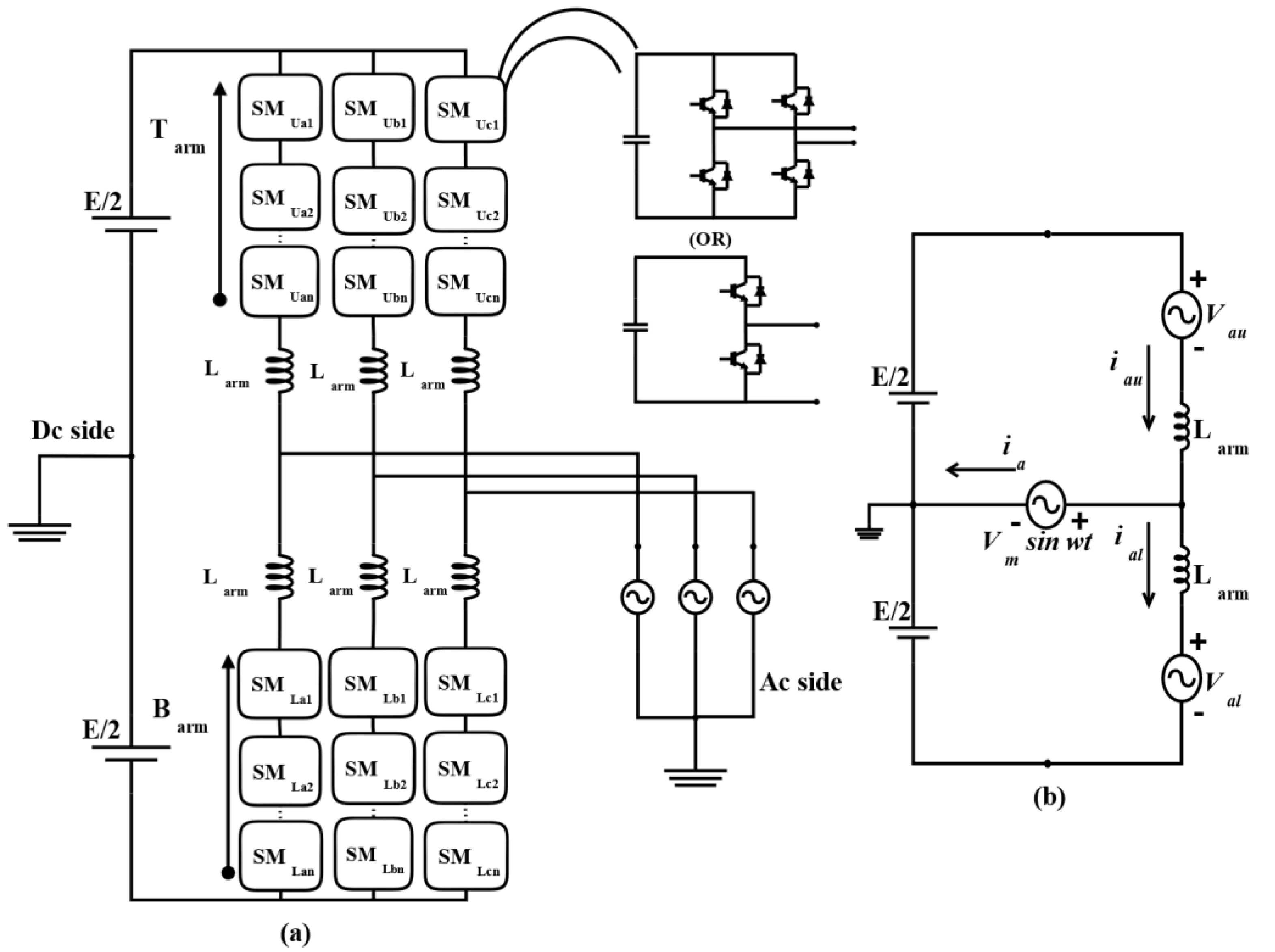
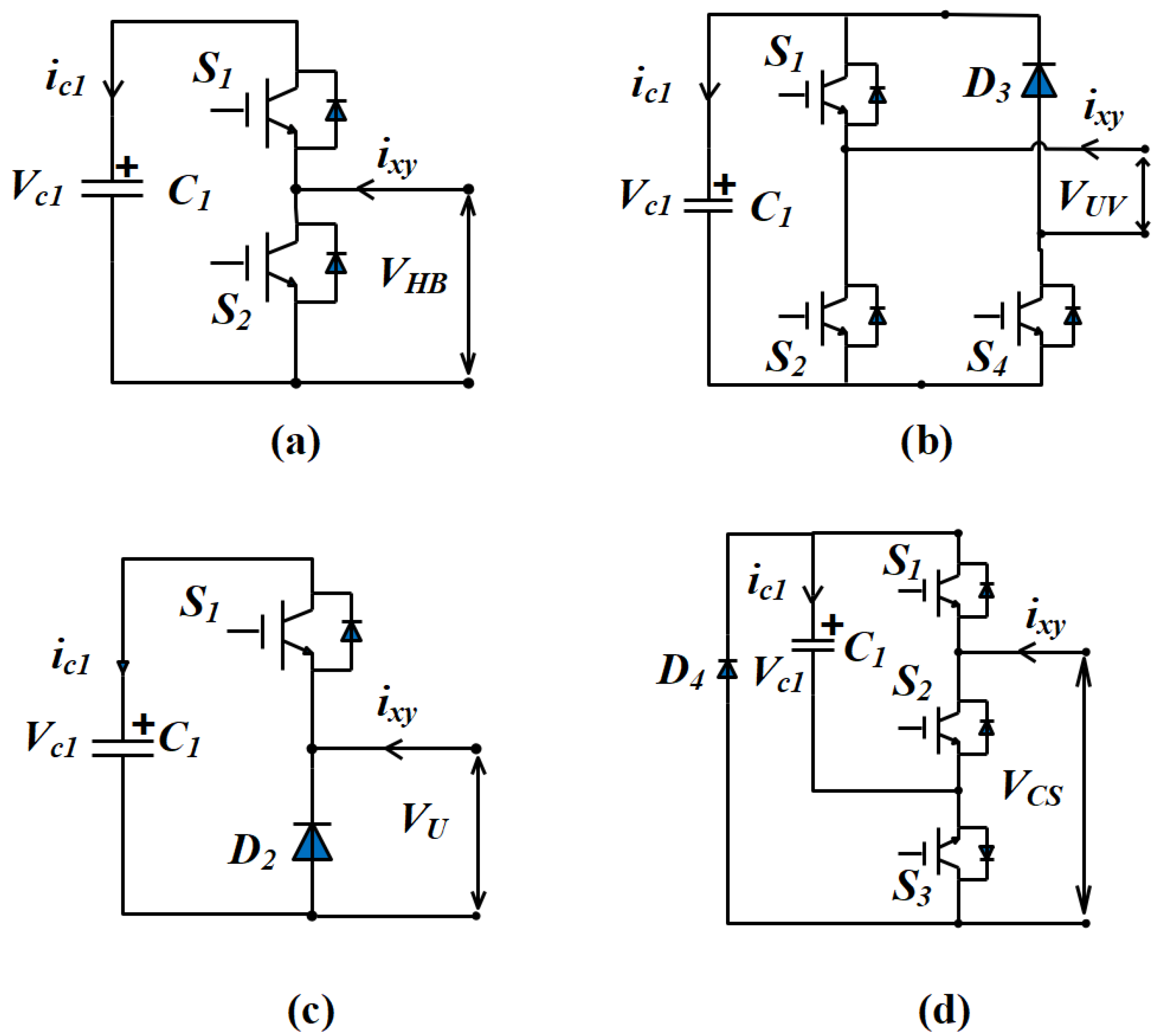
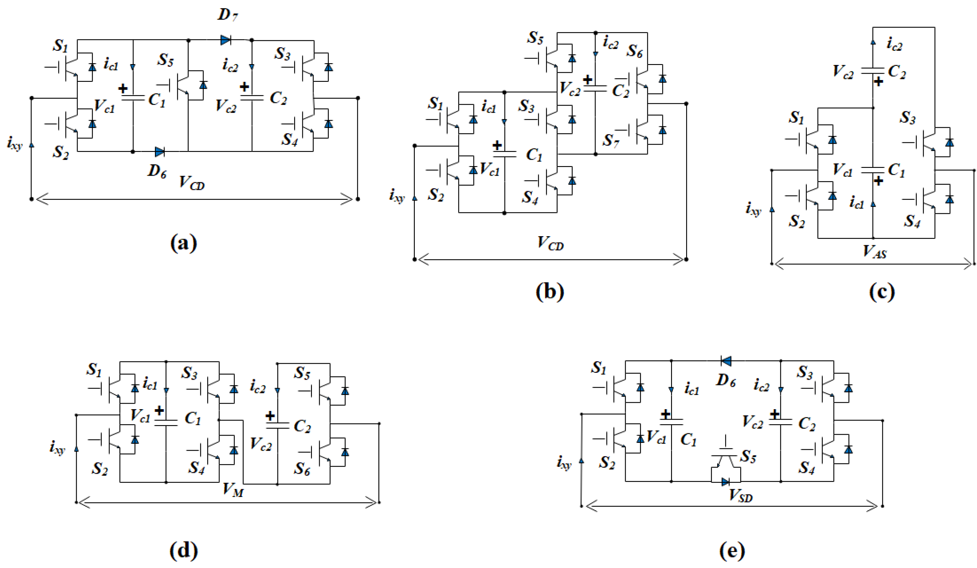
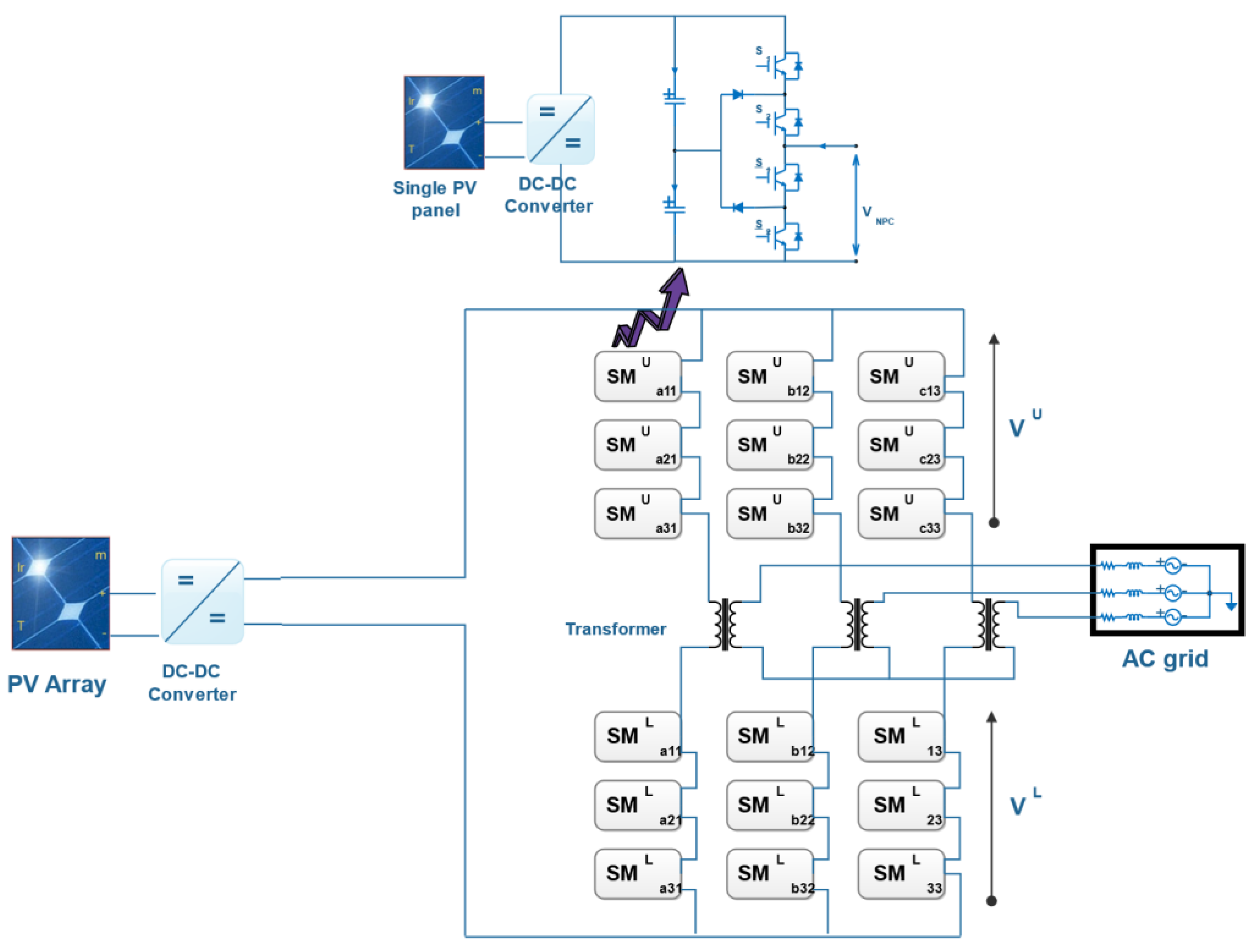
2. Modular Multilevel Converter and Sub Module Variants

Figure 1a is a three-phase MMC, and it consists of the top arm (Tarm) and the bottom arm (Barm). This arrangement generally could have an N-number of SM in each arm [11]. Each phase consists of arm inductors (Larm) and the submodules to provide better arm-currents without circulating harmonics and fault currents. Submodule (SM) or power cell represents a topological connection of IGBTs and could be of any voltage level. Generally, this SM is half-bridge (HBSM) or full-bridge (FBSM), but some researchers [12] started using SM with high levels. The SMs in the arms must be identical to get a symmetrical output wave. In the basic operation of the MMC, there is a chance of two events—sub-module insertion or by-passing state—whenever all the sub-modules are inserted in series and would result in arm voltages, respectively, and in turn produces a multilevel output. During the insertion processes, the SM capacitors were charged to their rated voltage magnitudes in the blocking mode based on the SM variants. The DC-link energy was equally divided among the SM capacitors; otherwise, there would be an unbalance of voltages and circulating currents within the phases. Figure 1b is a single-phase equivalent representation of a conventional MMC. The top and bottom arms’ SM’s total voltage magnitudes constitute V au and Val, respectively. For many applications, like motor drive, the number of SMs drastically increased day by day. The ongoing developer has structurally connected multilevel SM topologies to have dc fault handling capability, dimension reduction, and a higher number of voltage levels. Table 1 here provides us with the topological variants of SMs. Two-level SMs: Figure 2a shows the half-bridge submodule (HBSM) to produce the unipolar voltage by chopping the dc-link voltage. It consists of two IGBTs and a capacitor [13]. It can produce two levels of voltages 0, +VC1 when bypassed and inserted. In the HBSM, the dc voltage component will be present in the MMC arms [14]. Figure 2b is unipolar voltage FBSM [12], and this is similar to FBSM but with a slight replacement of a S3 switch with D3 of the FBSM (Figure 3a); it would be suitable for dc-fault handling capability. Another two-level variant is the unidirectional SM [15], and it has fewer semiconducting switches, as shown in Figure 2c. The clamp single submodule (CSSM) configuration is another configuration [16], which is shown in Figure 2d. The CSSM is derived from the three-level flying capacitor submodules (TLFCSM) for providing dc-fault handling capability during unidirectional operation.
Three-level SMs: The well-known FBSM [16] is depicted in Figure 3a, and it generates bipolar output voltage levels, and we can use this for bipolar operation systems [17]. Moreover, if we connect two FBSMs in parallel, we could have a four-quadrant operation [18]. From Figure 3e, we can see that the three-level flying capacitor sub-module (TLFCSM) [14,15,18] has two capacitors—C1 which is twice in voltage rating with C2. This configuration does not have dc-fault handling and computationally complex control [19,20]. We see a three-level neutral point clamped submodules (TLNPC) in Figure 3b,d,g [14,18,21]. SMs in Figure 3d and TLFCSM are structurally close and produce 0, +VC2, and +(VC1 + VC2) magnitudes; SM in Figure 3b contains four switches, two capacitors, and two diodes, whereas SM in Figure 3g has six switches and two capacitors. Figure 3d, SM will be formed by the two-series combination of commutation circuits, while Figure 3b can be possible with the T-connection of switches; the midpoint switch here can block the voltages in both directions [22].
Even though it has more components, it lacks the dc-link short circuit handling capability, which results in severe control losses [17]. Two FBSMs are connected, as shown in Figure 3c, for improving the capacitor voltage performance, while keeping their SM’s power level the same. This configuration [23] double-submodule (DSM) can improve the functionality of the SM without an increment in the semiconducting device’s cost. With this capacitor, voltage ripples at low frequencies could also be reduced. However, it lacks the presence of bipolar operation. In [12], another three-level cross-connected SM (TLCCSM,) formed by connecting two HBSMs back-to-back with switch and diode, is shown in Figure 3f. Making the connection like this, we could produce voltage magnitudes 0, VC1, and (VC1 + VC2). The diagonal-bridge SM (DBSM), shown in Figure 3i, is another variant that is similar to FBSM but with two diagonal switches that are replaced by diodes [24].
The last one is the three-level SM that is an improved hybrid SM (IHSM) [14], which has maximum voltage blocking of (VC1 + VC2), as depicted in Figure 3h. Four-level SMs: Figure 4a,b shows two kinds of double clamp submodules (CDSM) [12,14,21]. These configurations are the combination of two HBSMs connected in series. Here the switch S5 is on continuously, so it becomes two HBSMs connected in series under normal operating conditions. When the IGBTs are in blocking mode, both capacitors form either series or parallel connections in this CDSM. Further, this SM, operated as FBSM, has undergone different capacitor voltages as paralleled. To prevent this paralleling issue, diodes presented in that path could be replaced with IGBT switches. They would make another configuration, as shown in Figure 4b (CDSM); so far as losses are considered, CDSM is the combination of HBSM and FBSM. The alternate way of arranging commutation cells is shown in Figure 4c. This arrangement could be able to provide a dc-fault handling capability and can generate four voltage magnitudes. A combination of FBSM and HBSM would result in forming a hybrid submodule termed an asymmetrical SM [25], and it can perform both unipolar and bipolar operations, as shown in Figure 4d. The series connected double SM(SDSM) in shown in Figure 4e, which is obtained by connecting two HBSMs with S5 and D6 [26]. It has the capability of arc extension whenever a short circuit has taken place, and it could protect MMCs even when zero impedance current would have been taken place. Five-level SMs: As shown in Figure 5a, five-level cross-connected SM (FLCCSM) is the same as CDSM. Structurally FLCCSM is designed with two HBSMs in back-to-back cross-connection with the help of S5 and S6 [21,27]. Due to the two capacitors of the SM being connected in series, a blocking effect on the dc-fault current can be created. A different cross-connected SM (CCSM) [27] is shown in Figure 5b. It has a balanced bipolar voltage output, which could achieve greater voltage [28]. Similarly, if FBSMs are connected as parallel-connected SMs [29], which is shown in Figure 5c, they would give a reduced capacitor ripple.

3. Control Strategy of the Proposed MMC

The main part is the SM, which is may be a DC-DC or DC-AC power converter. Selection of better SM can provide fair control complexity, voltage blocking capability, and bipolar operation at a minimal cost. A new circuit performance of MMC with HB-SM is discussed in [2] by interchanging inductors with a transformer and also it offers twice the DC-AC voltage gain. The conventional MMC is having the advantage of power devices voltage ratings are halved, and the capacitor size of the SM is also lessened.
This paper uses neutral point clamped (NPC) SMs for the converter arrangement. The schematic (Figure 6) of the proposed MMC has slightly changed the SM with NPC SM with every single PV-panel, and the DC-DC converter and the DC-link to the MMC has been maintained by the PV array followed with the DC-DC converter. Figure 7 shows the controlling structure. For this controller implementation, initially, we are sensing the line-to-line three-phase voltages, and then these are transformed to two-phase voltage quantities by alpha-beta park’s transformation. Using these alpha-beta voltages, PLL is implemented, alpha-beta voltages are then converted into dq voltages using Clark’s transformation. Now from here, we are sensing the inverter side currents for the controller implementation. These currents are then transformed to the alpha-beta domain using park’s transformation and then transformed to the dq domain using Clark’s transformation. Here, Id corresponds to active current, and Iq corresponds to reactive current. Later Id&Iq are then subtracted from reference currents to find the error, and the error is fed to the PI controller to produce Eq and Ed. It is then transformed to abc voltages to get the references for PWM generation and, finally, we get the PWM generation block.
Generally, arm components in the traditional MMC are designed using the following equations.
L a r m · C a r m = 1 ω 2 { 2 ( h 2 1 ) + m 2 h 2 8 h 2 ( h 2 1 ) }
C a r m = 1 L a r m · ω 2 { 2 ( h 2 1 ) + m 2 h 2 8 h 2 ( h 2 1 ) }
where ω is the operating frequency, h is the harmonic order, and m is the modulation index.
However, in the proposed strategy, we use the transformers instead of arm inductors in the traditional MMC.
( L a r m + m u t u a l   i n d u c a n c e ) · C a r m = 1 ω 2 { 2 ( h 2 1 ) + m 2 h 2 8 h 2 ( h 2 1 ) }
From Equations (1) and (3), the inductance component is more in the proposed strategy, because of the mutual inductance of the transformer when compared to the traditional MMC for the same harmonic order and modulation index. Hence, from Equations (2) and (4), the proposed system requires a lesser value of capacitance when compared to the traditional MMC.

4. Modulation Strategies

Pulse width modulation (PWM) is generally used for regulating the power converter AC output voltage. The desired (reference) AC output voltage is achieved by regulating the duty cycle of the switching equipment. PWM methods were intended to eliminate harmonic components in the output voltage and increase the magnitude of the output voltage at any switching frequency. Figure 8 demonstrates the classification of various pulse width modulation techniques commonly used in multilevel converters. These are the PWM techniques adopted in VSC applications based on the switching frequency requirements. Figure 9 shows the simulation results with the (a) Sine PWM with the level-shifted carrier (SPWMLSC), (b) Sine PWM with the phase-shifted carrier (SPWMPSC), (c) Sine with the third harmonic injected level-shifted carrier (STHILSC), and (d) Sine with the third harmonic injected phase-shifted carrier (STHIPSC).

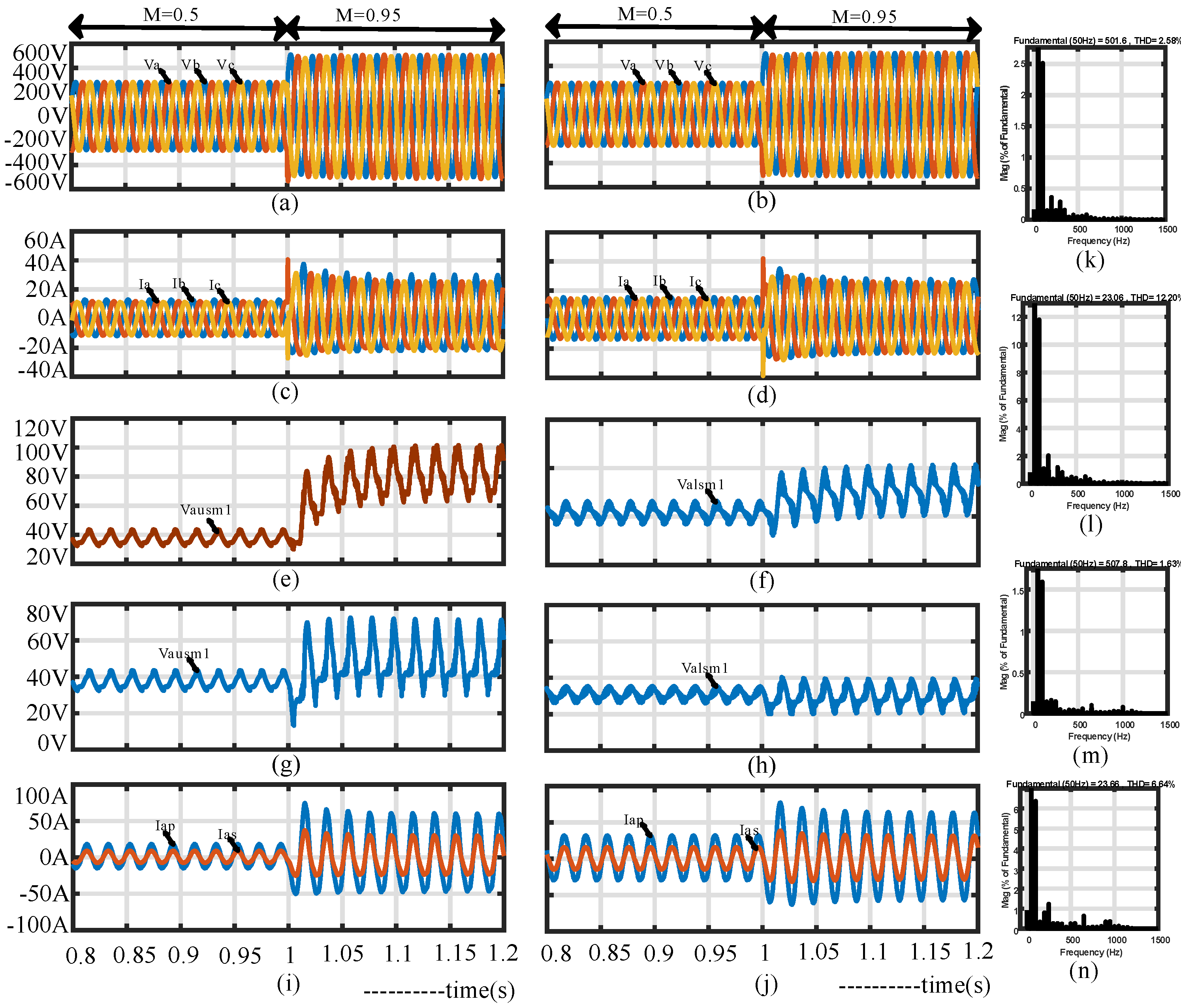
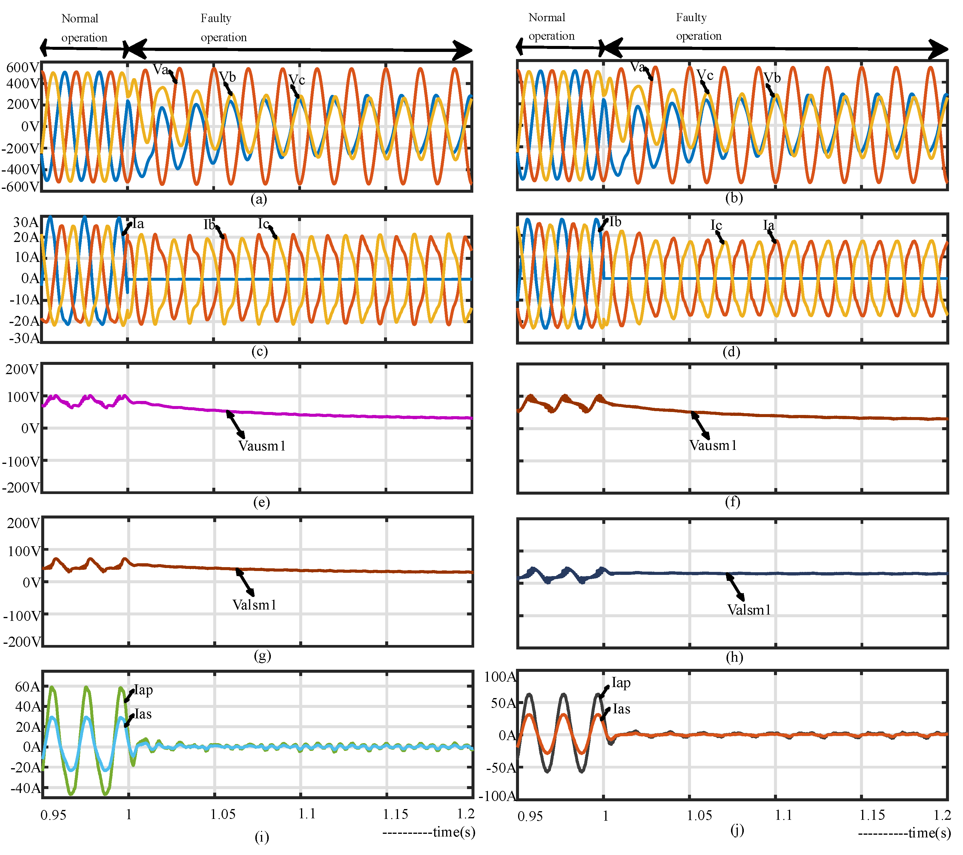
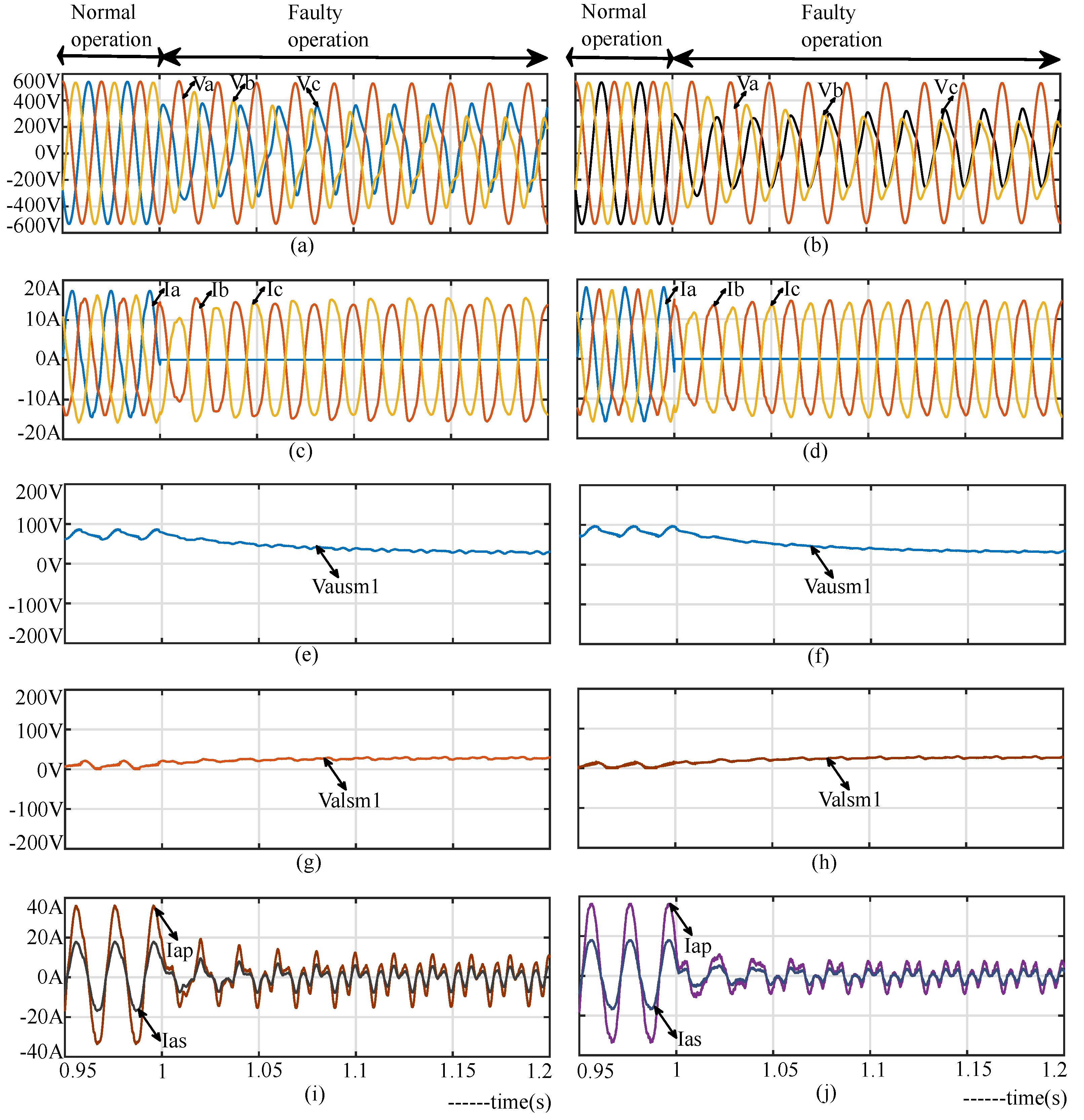
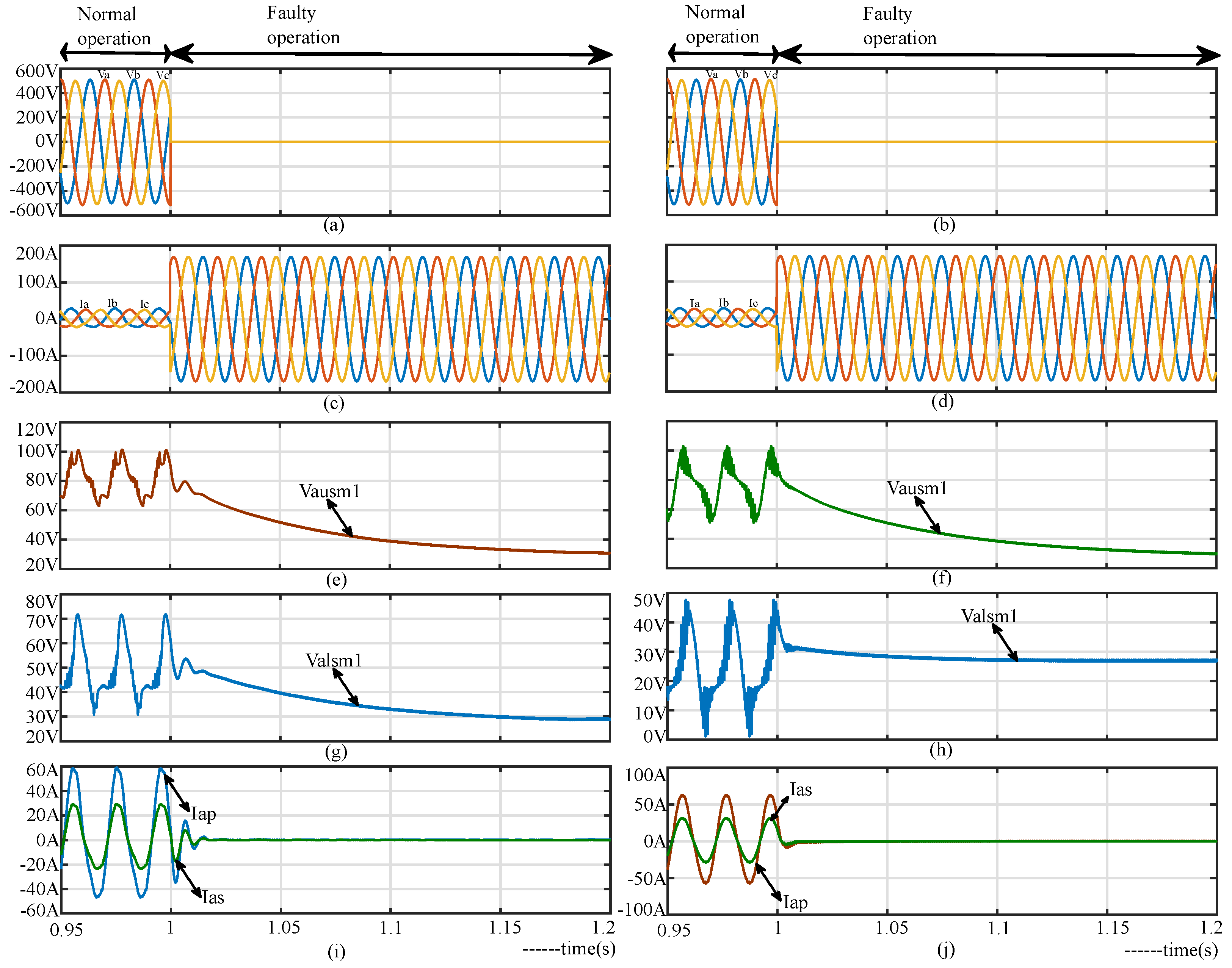
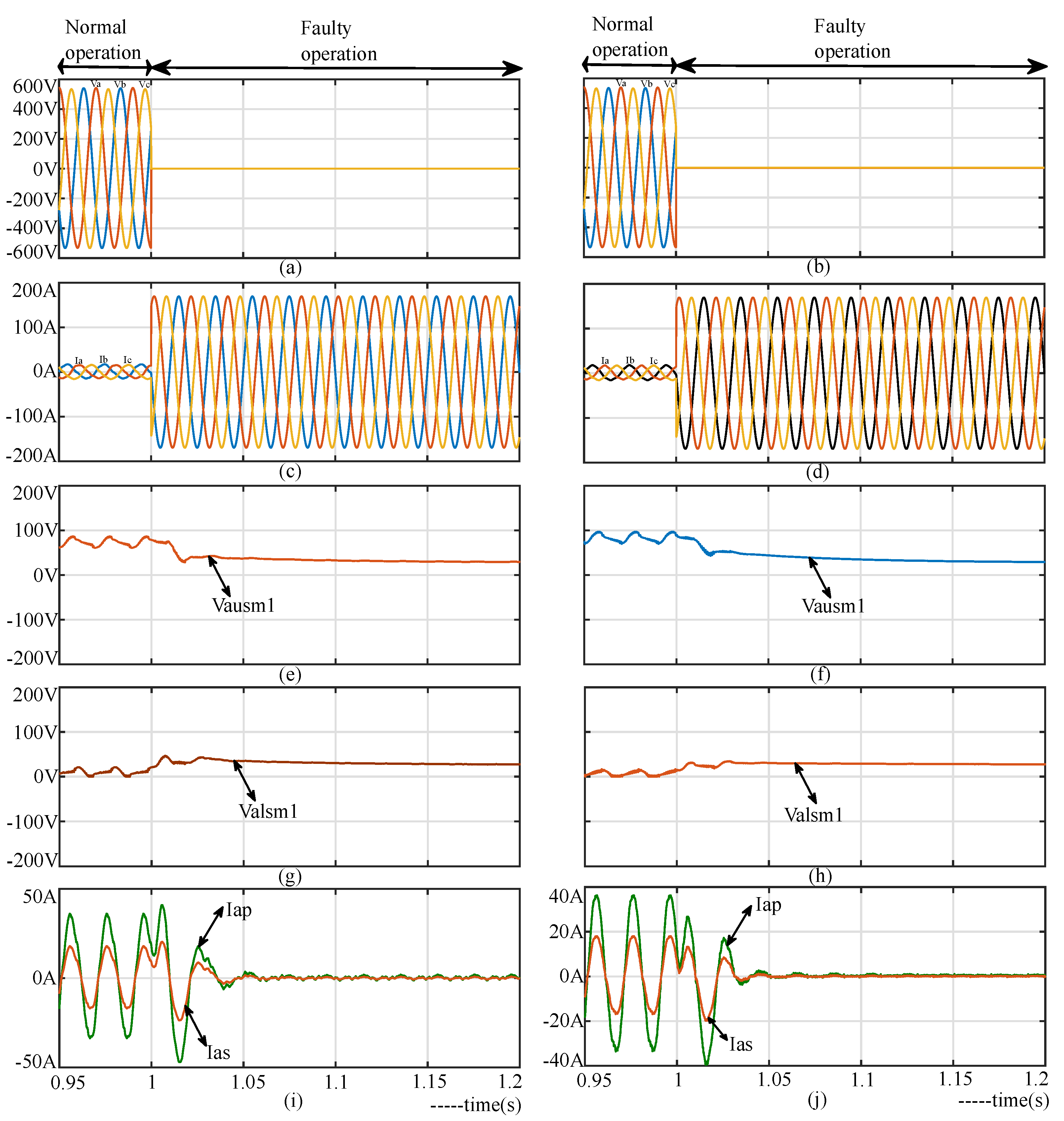
5. Results and Discussion

The simulation results of the proposed converter with various PWM schemes are clearly explained in this section. The parameters chosen for the simulation are given in Table 2. From Figure 10, we can see that the converter is operated with a modulation index (MI) of 0.5 from t = 0.8 s to t = 1.2 s, and it is operated with M = 0.95 from t = 0.8 s to t = 1.2 s. It is observed from Figure 10a,k that the THD in line voltage of the converter with d-q control and SPWMLSC is 2.58% at 50 Hz. respectively. In addition, from Figure 10b,m, the THD in line voltage of the converter with d-q control and SPWMPSC is 1.63%. Similarly, the THD in line current with d-q control and SPWMLSC is 12.20% and with SPWMPSC is 6.64% at 50 Hz, as shown in Figure 10c,l, respectively. Figure 10e,g shows the capacitor voltages of upper arm phase-a SM-1 and lower arm phase-a SM-1 with SPWMLSC modulation scheme. Figure 10f,h shows the capacitor voltages of the upper arm phase-a SM-1 and lower arm phase-a SM-1 with SPWMPSC modulation scheme. Figure 10i,j shows the transformer primary and secondary phase-a currents for both PWM techniques, respectively.
Further, the converter’s dynamic performance is analyzed when there is a step-change from time t = 1 s to t = 1.2 s in the current magnitude of I = 7.25 A to I = 17.5 A at 50 Hz frequency. It is observed from Figure 11a,k that the THD in line voltage of the converter with d-q control and STHILSC is 1.26% at 50 Hz, respectively, and from Figure 11b,m the THD in line voltage of the converter with d-q control and STHIPSC is 1.18%. Similarly, the THD in line current with d-q control and STHILSC is 10.26% and with STHIPSC is 8.84% at 50 Hz, as is shown in Figure 11c,l and Figure 11d,n respectively. Figure 11e,g shows the capacitor voltages of upper arm phase-a SM-1 and lower arm phase-a SM-1 with STHILSC modulation scheme. Figure 11f,h shows the capacitor voltages of upper arm phase-a SM-1 and lower arm phase-a SM-1 with STHIPSC modulation scheme. Figure 11i,j shows the transformer primary and secondary phase-a currents for both STHILSC and STHIPSC PWM techniques, respectively.
Now, the performance of the MMC is analyzed when it is operating in open and short circuit conditions. The Figure 12a,b shows the line voltages with d-q control and SPWMLSC and SPWMPSC respectively, when one of the phases is open-circuited from time t = 1 s to t = 1.2 s at 50 Hz frequency. Figure 12c,d is the line currents with d-q control and SPWMLSC and SPWMPSC. During the faulty open-circuited operation, Figure 12e–h shows the capacitor voltages of the upper arm and lower arm of phase-a SM-1 with SPWMLSC and SPWMPSC modulation schemes, respectively. Further, the primary and secondary phase-a transformer currents, when SPWMLSC and SPWMPSC schemes are implemented, are shown, respectively, in Figure 12i,j. Similarly, Figure 13a,b shows the line voltages with d-q control and STHILSC and STHIPSC respectively, when one of the phases is open-circuited from time t = 1 s to t = 1.2 s at 50 Hz. Figure 13c,d shows the line currents with d-q control and STHILSC and STHIPSC respectively. During the faulty open circuit condition, Figure 13e–h shows the STHILSC implemented upper arm and lower arm phase-a SM-1 capacitor voltages, respectively, and STHIPSC implemented upper arm and lower arm phase-a SM-1 capacitor voltages, respectively. The primary and secondary phase-a transformer currents when implementing STHILSC STHIPSC are shown in Figure 13i,j. Further, the short circuit condition is created from time t = 1 s to t = 1.2 s. At this time interval, the converter performance is visualized, with simulation results shown in Figure 14. Figure 14a,b shows the line voltages with d-q control and SPWMLSC and SPWMPSC respectively. Furthermore, Figure 14c,d shows the line currents with d-q control and SPWMLSC and SPWMPSC respectively. During the faulty short circuit condition, Figure 14e–h shows the upper arm mad lower arm phase-a SM-1 capacitor voltages with SPWMPSC and SPWMLSC schemes, respectively. Furthermore, the primary and secondary phase-a transformer currents SPWMLSC and SPWMPSC modulation schemes are shown in Figure 14i,j, respectively.
Here, the proposed converter’s performance is analyzed with sin third harmonic injection for both levels—shifted and phase-shifted PWM schemes—when the converter has been short-circuited from t = 1 s to t = 1.2 s at 50 Hz. Figure 15a,b shows the line voltages with d-q control and STHILSC and STHIPSC respectively. Figure 15c,d shows the line currents with d-q control and STHILSC and STHIPSC respectively. During short-circuited operation, Figure 15e–h shows the capacitor voltages of the upper arm and lower arm phase-a SM-1 with STHILSC modulation scheme. The primary and secondary phase-a transformer currents with STHILSC and STHIPSC schemes are shown in Figure 15i,j respectively.

6. Conclusions

In this paper the performance of the proposed MMC with NPC sub-modules in PV grid-connected applications was investigated under steady and transient conditions by employing various PWM techniques. The proposed MMC with NPC sub-modules with various SPWMLSC, SPWMPSC, STHILSC, and STHIPSC modulation techniques reports the voltage THDs were 2.58%, 1.63%, 1.26%, and 1.18%, and the current THDs were 12.20%, 6.64%, 10.26%, and 8.84%, respectively. The phase-shifted carrier modulation scheme has features like a low computational burden, can manage fault tolerance, and provides superior voltage balance under abnormal conditions when it comes to the digital controllers. From the results it is clearly revealed that the modulation schemes, such as STHILSC and STHIPSC, give superior performance in terms of lower output voltage and current harmonic distortions. The proposed arrangement achieves any volage level with lower rating of power switches when compared to the conventional neutral point clamped converter. This strategy can also significantly reduce the requirement of the high rating capacitor bank due to the presence of the mutual inductance component in the transformers, which is not present in the traditional MMC. Hence it can used for many high-power and medium-voltage grid-connected applications.

Author Contributions

Conceptualization—S.M. and R.V.K; Methodology, Software, Validation—S.M., R.V.K., P.V.B., and T.S.; Investigation, Resources, Writing—Original Draft Preparation, Writing—Review and Editing, Visualization; Supervision; Project Administration, S.M., R.V.K., P.V.B., and T.S. All authors have read and agreed to the published version of the manuscript.

Funding

The authors gratefully acknowledge the support offered by the Science and Engineering Research Board (SERB), Department of Science and Technology, Government of India, under the Grant number: ECR/2017/000316 for this research work.

Institutional Review Board Statement

Not applicable.

Informed Consent Statement

Not applicable.

Data Availability Statement

Not applicable.

Conflicts of Interest

The authors declare no conflict of interest.

References

  1. Mei, J.; Xiao, B.; Shen, K.; Tolbert, L.M.; Zheng, J.Y. Modular multilevel inverter with new modulation method and its application to photovoltaic grid-connected generator. IEEE Trans. Power Electron. 2013, 28, 5063–5073. [Google Scholar] [CrossRef]
  2. Nademi, H.; Das, A.; Burgos, R.; Norum, L.E. A new circuit performance of modular multilevel inverter suitable for photovoltaic conversion plants. IEEE J. Emerg. Sel. Top. Power Electron. 2015, 4, 393–404. [Google Scholar] [CrossRef]
  3. Rojas, C.A.; Kouro, S.; Perez, M.A.; Echeverria, J. DC–DC MMC for HVDC grid interface of utility-scale photovoltaic conversion systems. IEEE Trans. Ind. Electron. 2017, 65, 352–362. [Google Scholar] [CrossRef]
  4. Wu, P.; Huang, W.; Tai, N. Novel grid connection interface for utility-scale PV power plants based on MMC. J. Eng. 2019, 2019, 2683–2686. [Google Scholar] [CrossRef]
  5. Bayat, H.; Yazdani, A. A power mismatch elimination strategy for an MMC-based photovoltaic system. IEEE Trans. Energy Convers. 2018, 33, 1519–1528. [Google Scholar] [CrossRef]
  6. Acharya, A.B.; Ricco, M.; Sera, D.; Teoderscu, R.; Norum, L.E. Performance analysis of medium-voltage grid integration of PV plant using modular multilevel converter. IEEE Trans. Energy Convers. 2019, 34, 1731–1740. [Google Scholar] [CrossRef]
  7. Basu, T.S.; Maiti, S. A hybrid modular multilevel converter for solar power integration. IEEE Trans. Ind. Appl. 2019, 55, 5166–5177. [Google Scholar] [CrossRef]
  8. Bayat, H.; Yazdani, A. A hybrid MMC-based photovoltaic and battery energy storage system. IEEE Power Energy Technol. Syst. J. 2019, 6, 32–40. [Google Scholar] [CrossRef]
  9. Verdugo, C.; Candela, J.I.; Blaabjerg, F.; Rodriguez, P. Three-phase isolated multi-modular converter in renewable energy distribution systems. IEEE J. Emerg. Sel. Top. Power Electron. 2019, 8, 854–865. [Google Scholar] [CrossRef]
  10. Zhang, X.; Wang, M.; Zhao, T.; Mao, W.; Hu, Y.; Cao, R. Topological comparison and analysis of medium-voltage and high-power direct-linked PV inverter. CES Trans. Electr. Mach. Syst. 2019, 3, 327–334. [Google Scholar] [CrossRef]
  11. Solas, E.; Abad, G.; Barrena, J.A.; Aurtenetxea, S.; Carcar, A.; Zając, L. Modular multilevel converter with different submodule concepts—Part I: Capacitor voltage balancing method. IEEE Trans. Ind. Electron. 2012, 60, 4525–4535. [Google Scholar] [CrossRef]
  12. Solas, E.; Abad, G.; Barrena, J.A.; Aurtenetxea, S.; Carcar, A.; Zajac, L. Modular Multilevel Converter With Different Submodule Concepts—Part II: Experimental Validation and Comparison for HVDC Application. IEEE Trans. Ind. Electron. 2012, 60, 4536–4545. [Google Scholar] [CrossRef]
  13. Saad, H.; Dennetière, S.; Mahseredjian, J.; Delarue, P.; Guillaud, X.; Peralta, J.; Nguefeu, S. Modular multilevel converter models for electromagnetic transients. IEEE Trans. Power Deliv. 2013, 29, 1481–1489. [Google Scholar] [CrossRef]
  14. Dekka, A.; Wu, B.; Fuentes, R.L.; Perez, M.; Zargari, N.R. Evolution of topologies, modeling, control schemes, and applications of modular multilevel converters. IEEE J. Emerg. Sel. Top. Power Electron. 2017, 5, 1631–1656. [Google Scholar] [CrossRef]
  15. Jacobson, B.; Karlsson, P.; Asplund, G.; Harnefors, L.; Jonsson, T. VSC-HVDC Transmission with Cascaded Two-Level Converters. Proceeding of CIGRE SC B4 Session, Paris, France, 22 August 2010; pp. 1–8. [Google Scholar]
  16. Qin, J.; Saeedifard, M.; Rockhill, A.; Zhou, R. Hybrid design of modular multilevel converters for HVDC systems based on various submodule circuits. IEEE Trans. Power Deliv. 2014, 30, 385–394. [Google Scholar] [CrossRef]
  17. de Sousa, G.J.M.; Dias, A.D.S.; Alves, J.A.; Heldwein, M.L. June. In Modeling and control of a modular multilevel converter for medium voltage drives rectifier applications. In Proceedings of the 2015 IEEE 24th International Symposium on Industrial Electronics (ISIE), Buzios, Brazil, 3–5 June 2015; pp. 1080–1087. [Google Scholar]
  18. Xu, J.; Zhao, P.; Zhao, C. Reliability analysis and redundancy configuration of MMC with hybrid submodule topologies. IEEE Trans. Power Electron. 2015, 31, 2720–2729. [Google Scholar] [CrossRef]
  19. Perez, M.A.; Bernet, S.; Rodriguez, J.; Kouro, S.; Lizana, R. Circuit topologies, modeling, control schemes, and applications of modular multilevel converters. IEEE Trans. Power Electron. 2014, 30, 4–17. [Google Scholar] [CrossRef]
  20. Nami, A.; Liang, J.; Dijkhuizen, F.; Demetriades, G.D. Modular multilevel converters for HVDC applications: Review on converter cells and functionalities. IEEE Trans. Power Electron. 2014, 30, 18–36. [Google Scholar] [CrossRef]
  21. Debnath, S.; Qin, J.; Bahrani, B.; Saeedifard, M.; Barbosa, P. Operation, control, and applications of the modular multilevel converter: A review. IEEE Trans. Power Electron. 2014, 30, 37–53. [Google Scholar] [CrossRef]
  22. Soeiro, T.B.; Kolar, J.W. Novel 3-level hybrid neutral-point-clamped converter. In Proceedings of the IECON 2011-37th Annual Conference of the IEEE Industrial Electronics Society, Melbourne, VIC, Australia, 7–10 November 2011; pp. 4457–4462. [Google Scholar]
  23. Ilves, K.; Taffner, F.; Norrga, S.; Antonopoulos, A.; Harnefors, L.; Nee, H.P. A submodule implementation for parallel connection of capacitors in modular multilevel converters. IEEE Trans. Power Electron. 2014, 30, 3518–3527. [Google Scholar] [CrossRef]
  24. Yu, X.; Wei, Y.; Jiang, Q.; Xie, X.; Liu, Y.; Wang, K. A novel hybrid-arm bipolar MMC topology with DC fault ride-through capability. IEEE Trans. Power Deliv. 2016, 32, 1404–1413. [Google Scholar] [CrossRef]
  25. Mao, M.; Ding, Y.; Chang, L.; Hatziargyriou, N.D.; Chen, Q.; Tao, T.; Li, Y. Multi-objective power management for EV fleet with MMC-based integration into smart grid. IEEE Trans. Smart Grid 2017, 10, 1428–1439. [Google Scholar] [CrossRef]
  26. Zhang, J.; Zhao, C. The research of SM topology with DC fault tolerance in MMC-HVDC. IEEE Trans. Power Deliv. 2015, 30, 1561–1568. [Google Scholar] [CrossRef]
  27. Nami, A.; Wang, L.; Dijkhuizen, F.; Shukla, A. September. In Five level cross connected cell for cascaded converters. In Proceedings of the 2013 15th European conference on power electronics and applications (EPE), Lille, France, 2–6 September 2013; pp. 1–9. [Google Scholar]
  28. Abd Razak, A.B. Modulation Strategy for New Asymmetrical Multilevel Inverter Topology Using Nearest Dc Level. Ph.D. Thesis, Universiti Teknologi Malaysia, Skudai, Malaysia, 2019. [Google Scholar]
  29. Chaudhuri, T. Cross connected multilevel voltage source inverter topologies for medium voltage applications. Ph.D. Dissertation, EPFL, Lausanne, Switzerland, 2008. [Google Scholar]
Figure 1. (a) Configuration of three-phase MMC, (b) single-phase equivalent circuit of conventional MMC.
Applsci 12 01219 g001
Figure 2. Two-level submodule variants (a) Half-bridge (b) Unipolar voltage full-bridge (c) Unidirectional SM (d) Clamp single SM.
Applsci 12 01219 g002
Figure 3. Three-level submodule variants (a) Full-bridge SM (b) Three-level flying capacitor submodule (TLFCSM) (c) TLNPC-1 (d) TLNPC-2 (e) TLNPC-3 (f) double-submodule (DSM) (g) three-level cross-connected (TLCCSM) (h) Improved hybrid SM(IHSM) (i) Diagonal-bridge SM (DBSM).
Applsci 12 01219 g003
Figure 4. Four-level submodule variants (a) Clamp Double Submodules (CDSM), (b) Clamp Double Submodules (CDSM), (c) Mixed SM, (d) Asymmetrical SM, (e) Series Connected Double SM (SDSM).
Applsci 12 01219 g004
Figure 5. Five-level submodule variants (a) Five-Level Cross-Connected SM(FLCCSM), (b) Cross-Connected SM(CCSM), (c) Parallel-Connected SM.
Applsci 12 01219 g005
Figure 6. Schematic of the proposed modular multilevel converter.
Applsci 12 01219 g006
Figure 7. Control block diagram.
Applsci 12 01219 g007
Figure 8. General pulse width modulation classification based on switching frequency.
Applsci 12 01219 g008
Figure 9. Modulation schemes conducted on this converter. (a) Sine PWM with level-shifted carrier (SPWMLSC); (b) Sine PWM with phase-shifted carrier (SPWMPSC); (c) Sine with third harmonic injected level-shifted carrier (STHILSC); and (d) Sine with third harmonic injected phase-shifted carrier (STHIPSC).
Applsci 12 01219 g009
Figure 10. Change in modulation index. (a) Line voltages of converter with d-q control and SPWMLSC, (b) line voltages of converter with d-q control and SPWMPSC, (c) Line currents of converter with d-q control and SPWMLSC, (d) line currents of converter with d-q control and SPWMPSC, (e) SPWMLSC implemented upper arm phase-a SM-1 capacitor voltage, (f) SPWMPSC implemented upper arm phase-a SM-1 capacitor voltage, (g) SPWMLSC implemented lower arm phase-a SM-1 capacitor voltage, (h) SPWMPSC implemented lower arm phase-a SM-1 capacitor voltage, (i) primary and secondary phase-a transformer currents when SPWMLSC is implemented, (j) primary and secondary phase-a transformer currents when SPWMPSC is implemented, (k) SPWMLSC implemented line voltage THD, (l) SPWMLSC implemented line current THD, (m) SPWMPSC implemented line voltage THD, and (n) SPWMPSC implemented line current THD.
Applsci 12 01219 g010
Figure 11. Change in current. (a) Line voltages of converter with d-q control and STHILSC, (b) line voltages of converter with d-q control and STHIPSC, (c) line currents of converter with d-q control and STHILSC, (d) line currents of converter with d-q control and STHIPSC, (e) STHILSC implemented upper arm phase-a SM-1 capacitor voltage, (f) STHIPSC implemented upper arm phase-a SM-1 capacitor voltage, (g) STHILSC implemented lower arm phase-a SM-1 capacitor voltage, (h) STHIPSC implemented lower arm phase-a SM-1 capacitor voltage, (i) primary and secondary phase-a transformer currents when STHILSC is implemented, (j) primary and secondary phase-a transformer currents when STHIPSC is implemented, (k) STHILSC implemented line voltage THD, (l) STHILSC implemented line current THD, (m) STHIPSC implemented line voltage THD, and (n) STHIPSC implemented line current THD.
Applsci 12 01219 g011
Figure 12. Converter when one phase is open circuited. (a) Line voltages of converter with d-q control and SPWMLSC, (b) line voltages of converter with d-q control and SPWMPSC, (c) line currents of converter with d-q control and SPWMLSC, (d) line currents of converter with d-q control and SPWMPSC, (e) SPWMLSC implemented upper arm phase-a SM-1 capacitor voltage, (f) SPWMPSC implemented upper arm phase-a SM-1 capacitor voltage, (g) SPWMLSC implemented lower arm phase-a SM-1 capacitor voltage, (h) SPWMPSC implemented lower arm phase-a SM-1 capacitor voltage, (i) primary and secondary phase-a transformer currents when SPWMLSC is implemented, (j) primary and secondary phase-a transformer currents when SPWMPSC is implemented.
Applsci 12 01219 g012
Figure 13. Converter when one phase is open circuited. (a) Line voltages of converter with d-q control and STHILSC, (b) line voltages of converter with d-q control and STHIPSC, (c) line currents of converter with d-q control and STHILSC, (d) line currents of converter with d-q control and STHIPSC, (e) STHILSC implemented upper arm phase-a SM-1 capacitor voltage, (f) STHIPSC implemented upper arm phase-a SM-1 capacitor voltage, (g) STHILSC implemented lower arm phase-a SM-1 capacitor voltage, (h) STHIPSC implemented lower arm phase-a SM-1 capacitor voltage, (i) primary and secondary phase-a transformer currents when STHILSC is implemented, (j) primary and secondary phase-a transformer currents when STHIPSC is implemented.
Applsci 12 01219 g013
Figure 14. Converter during short circuited condition. (a) Line voltages of converter with d-q control and SPWMLSC, (b) line voltages of converter with d-q control and SPWMPSC, (c) line currents of converter with d-q control and SPWMLSC, (d) line currents of converter with d-q control and SPWMPSC, (e) SPWMLSC implemented upper arm phase-a SM-1 capacitor voltage, (f) SPWMPSC implemented upper arm phase-a SM-1 capacitor voltage, (g) SPWMLSC implemented lower arm phase-a SM-1 capacitor voltage, (h) SPWMPSC implemented lower arm phase-a SM-1 capacitor voltage, (i) primary and secondary phase-a transformer currents when SPWMLSC is implemented, (j) primary and secondary phase-a transformer currents when SPWMPSC is implemented.
Applsci 12 01219 g014
Figure 15. Converter during short circuited condition. (a) Line voltages of converter with d-q control and STHILSC, (b) line voltages of converter with d-q control and STHIPSC, (c) line currents of converter with d-q control and STHILSC, (d) line currents of converter with d-q control and STHIPSC, (e) STHILSC implemented upper arm phase-a SM-1 capacitor voltage, (f) STHIPSC implemented upper arm phase-a SM-1 capacitor voltage, (g) STHILSC implemented lower arm phase-a SM-1 capacitor voltage, (h) STHIPSC implemented lower arm phase-a SM-1 capacitor voltage, (i) primary and secondary phase-a transformer currents when STHILSC is implemented, (j) primary and secondary phase-a transformer currents when STHIPSC is implemented.
Applsci 12 01219 g015
Table 1. Comparison of different submodules [13,14,15,16,17,18,19,20].
Sub-Module (SM)NVLVoltage LevelNSMNSCMBVBipolarDC-Fault Handling
Two-Level SMs
HBSM20, +VC121VC1NoNo
Unipolar SM20, +VC131VC1NoYes
Unidirectional20, +VC111VC1NoNo
CSSM20, +VC132VC1NoYes
Three-Level SMs
FBSM30, +VC1, −VC142VC1YesYes
TLFCSM30, +VC2, +(VC1 + VC2)42VC1 + VC2NoNo
TLNPC-130, +VC2, +(VC1 + VC2)42VC1 + VC2NoNo
TLNPC-230, +VC2, +(VC1 + VC2)62VC1 + VC2NoNo
TLNPC-330, +VC2, +(VC1 + VC2)42VC1 + VC2NoNo
DSM30, +VC2, +(VC1 + VC2)84VC1 + VC2NoYes
TLCCSM30, +VC2, +(VC1 + VC2)53VC1 + VC2NoYes
DBSM30, +VC1, −VC221VC1YesYes
IHSM30, +VC1, +(VC1 + VC2)53VC1 + VC2NoYes
Four-Level SMs
CDSM-140, +VC1, +(VC1 + VC2)53VC1 + VC2YesYes
CDSM-240, +VC2, +(VC1 + VC2)73VC1 + VC2YesYes
Asymmetrical40, +VC2, +(VC1 + VC2)42VC1 + VC2YesYes
Mixed SM40, +VC2, +(VC1 + VC2)63VC1 + VC2YesYes
SDSM40, +VC2, +(VC1 + VC2)53VC1 + VC2YesYes
Five-Level SMs
FLCCSM50, +VC1, +VC2, ±(VC1 + VC2)63VC1 + VC2YesYes
CCSM50, +VC1, +VC2, ±(VC1 + VC2)84VC1 + VC2YesYes
PCSM50, +VC1, +VC2, ±(VC1 + VC2)84VC1 + VC2YesYes
Note: SM—Submodule, NVLs—Number of Voltage Levels, NSs—Number of Switches, MNSC—Maximum Number of Switches in the Conduction Path.
Table 2. Simulated converter parameters.
Number of Cells in Each Arm3
Ac line inductor3 µH
Carrier frequency1 KHz
Transformer resistance74 m-ohm
Transformer inductor3.48 mH
Cell capacitance1000 µF
Publisher’s Note: MDPI stays neutral with regard to jurisdictional claims in published maps and institutional affiliations.

