Article

Improving Thickness Uniformity of Amorphous Oxide Films Deposited on Large Substrates by Optical Flux Mapping

Department of Electrical Engineering, Feng Chia University, Taichung 40724, Taiwan
*
Author to whom correspondence should be addressed.
Appl. Sci. 2022, 12(23), 11878; https://doi.org/10.3390/app122311878
Submission received: 2 November 2022 / Revised: 16 November 2022 / Accepted: 21 November 2022 / Published: 22 November 2022

Abstract

:
In this study, three amorphous oxide thin films are prepared by an electron beam evaporation combined with ion-assisted deposition technique. With the aid of optical flux mapping method, thin film thickness distribution with good uniformity can be obtained by appropriate coating masks. Three metal oxide single-layer thin films are SiO2, Ta2O5 and Nb2O5, respectively. These thin films were deposited on a substrate holder with a radius of 275 mm that was divided into five different segments. Based on the optical flux mapping method, we can effectively simulate the geometric dimensions of the coating mask and obtain the width of the coating mask at different segments. If the film thickness uniformity is a function of masking area and center angle, it is necessary to determine the thickness distribution of the different segments and use a surface profiler to accurately measure the film thickness. We analyzed the thickness uniformity of three oxide films deposited at five different segments. The experimental measurement results show that the deviation of thickness uniformity is 0.38% for SiO2, 0.36% for Ta2O5, and 0.15% for Nb2O5 thin films, respectively.

1. Introduction

In the era of rapid development of technology, the uniformity of film thickness is very important issue for large-area coatings. In particular, the error of optical coating thickness has achieved the nanometer level. Because considerable production and large-area manufacturing have become relatively important to reduce costs. How to control the film thickness in the evaporation process to achieve the theoretical design value is very critical. The uniformity of the film thickness is affected by the placement position between the evaporation source and the substrate, the vacuum value inside the chamber, and the emission characteristics of different materials which the different factors will have an impact [1]. These factors include substrate holder geometry, vacuum pressure, system temperature (i.e., substrate and material flux temperature), and angle configuration of deposition material and substrate [2].
In 2018, Ho et al. [3] proposed a novel spatial-distribution function of diffusion theory, which replaced Knudsen’s law of cosine and empirical rule. The thin film deposition of electron beam evaporation on the substrate was investigated. The thickness distribution obtained the accurate prediction of the deposition thickness of titanium and aluminum film confirms that this method has developed to improve the uniformity of the thin films. The most widely used method is to rotate the substrate holder to increase the uniform distribution of the film thickness, and also use a mask to obtained better film uniformity. But the disadvantages will cause material waste. Therefore, by optimizing the mask geometry can be obtained the best uniform distribution and the least loss of materials. In 2000, Villa et al. [4] designed a mask to be applied to large-area substrates of different geometric shapes and obtained a good film thickness distribution. In 2018, Wang et al. [5] used simulation modeling to compare different complex geometric structures. A new program for modelling and simulating thin film uniformity for physical vapor deposition was developed by using MathCAD. A mask for optimizing thin film thickness distribution designed using the program was shown to improve thickness uniformity from ±4% to ±0.56%. The advantage of electron beam evaporation is that the quality of the deposited film has higher purity, evaporation rate fast, and better control of film thickness [6]. For example, relevant applications include mirrors for gravitational wave detection [7], photovoltaic semiconductor industry, anti-reflection films [8], etc. Over the past decades, many methods have been developed to improve film thickness uniformity. The most widespread method is to achieve thickness uniformity through the substrate holder revolution or planetary rotation [9]. At the same time, the use of a modified coating mask can not only improve the film thickness uniformity, but also achieve the specified thickness distribution [10]. Basically, the modification of the coating mask requires time-consuming trial-and-error methods. In recent years, the application of physical deposition theory in the study of film thickness distribution and theoretical mask design has attracted more and more attention. The shape modification of the coating mask can improve the efficiency of material utilization.
For the formation of thin films using other different techniques, electrochemical synthesis is a promising method for preparing thin films with a given thickness and uniform phase composition [11]. The dependence of the structure, phase composition and thickness of the electrodeposited films was obtained. Due to different preparation methods, the substrates have different microstructures and surface properties. Zubar et al. [12] reported the effect of the structure and surface properties of the substrate on the composition gradient of NiFe films. Some results of the preparation and investigation of other substituted oxides promising for practical applications are reported in the literature. Zhumatayeva et al. [13] reported the results of a study of structural characteristics, as well as the possibility of using Li0.15Sr0.85TiO3 ceramics as anode materials for lithium-ion batteries. Some cases also show the importance of thin films for use against incident radiation. Trukhanov et al. [14] presented that magnetic properties and shielding characteristics were investigated as well as function of thickness and number of layers. Difference in magnetic properties for Ni80Fe20 films with different thickness is due to formation of defect layers on the top and bottom film surfaces during electrodeposition processes. They also studied the effect of hydrostatic pressure (up to 1.1 GPa) in wide temperature range of magnetic properties optimal doped La0.70Sr0.30MnO2.85 magnetic with oxygen vacancies [15]. In 2020, Kadyrzhanov et al. [16] devoted to assess the prospects of using CuBi2O4 composite films of various thicknesses as protective coatings against exposure to ionizing radiation. Owing to the advantages of nanomaterials, oxides with a spinel structure of the general formula AB2O4 are known as possible active materials for the energy storage device [17]. Ghiyasiyan-Arani et al. [18] reported morphology controlled the fabrication of AlV3O9 (AV) by surfactant-assisted hydrothermal method and the use of AV products were demonstrated as both positive and negative electrode in Li-ion batteries. They also investigated the effect of AlV3O9 as cathode materials in Li-ion batteries on the zero to two dimensional carbon nanostructures [19].
Based on the above literature discussion and research topics, these cases demonstrate that film thickness uniformity plays an important role in the effect of film properties. In general, optical coating technology requires thickness control in the range of ±1% to achieve reproducible performance. In this study, a novel flux mapping method based on 50 million ray tracing under electron beam evaporation is proposed for optical thin film deposition, and its intensity distribution is equivalent to film thickness accumulation. To the best of our knowledge, the optical flux mapping method has not been applied to the coating technology. This study breaks through the complex diffusion equation derivation and obtains the deposition curve of the equivalent film thickness of the substrate holder with one revolution. We can effectively simulate the geometry of the coating mask and obtain the width of the coating mask at different segments. This method can be used to quantitatively control the film thickness uniformity of large-area substrate and rapidly optimize the shape of the coating mask. Therefore, the proposed method greatly reduces the time and cost of coating process by simulating and optimizing the coating mask.

2. Methods

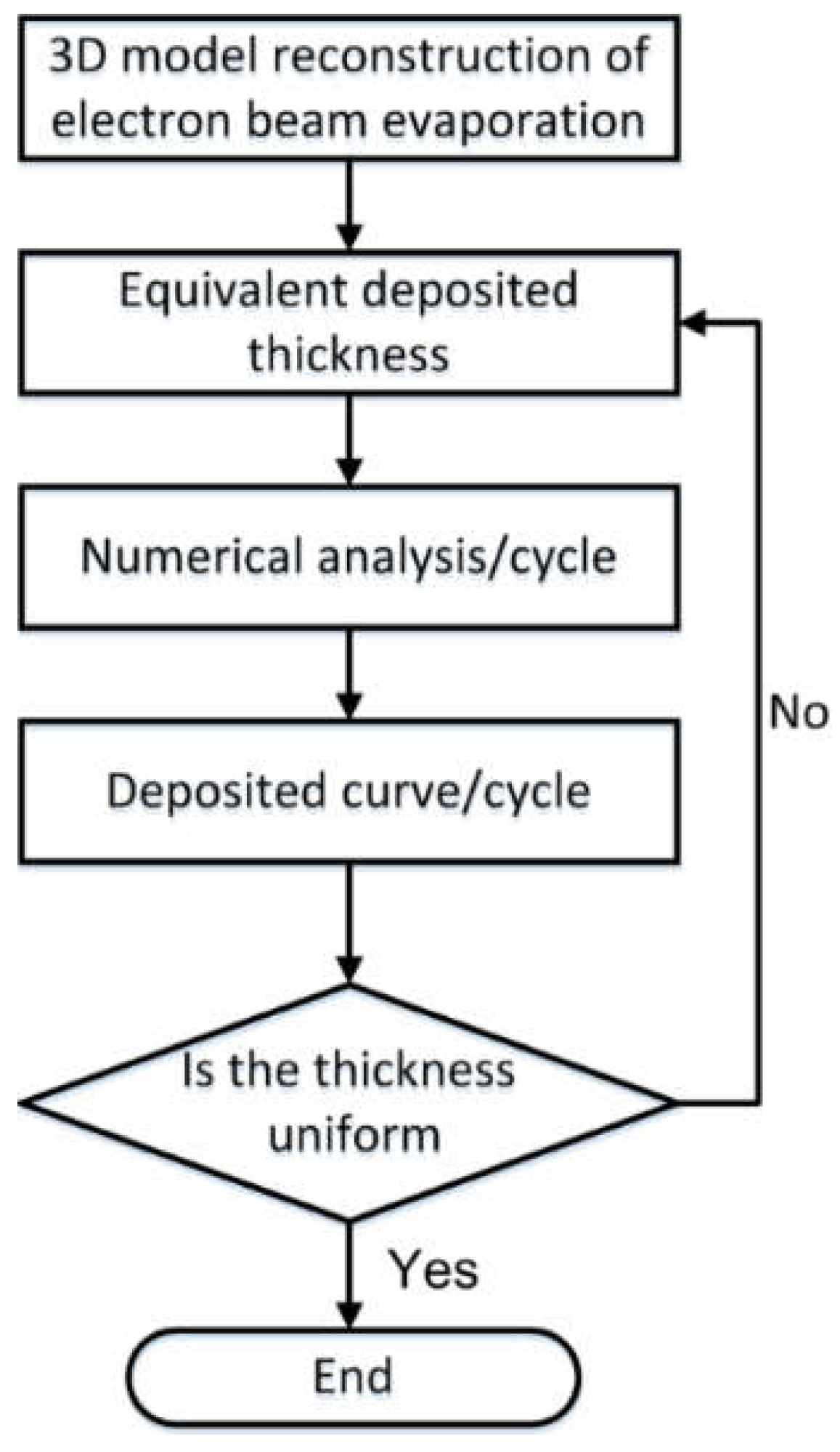
2.1. Thin Film Thickness Uniformity Simulation

The optical simulation software LightTools is used to reconstruct the 3-D model to restore the geometric position of the vapor deposition machine to the same scale. The geometric position is converted into a coordinate system. The flux intensity is obtained through a large number of light tracing methods which can equivalent to the thin film deposition process of electron gun vapor deposition. The simulation results of 50 million rays are compared with the experimental results. The coating holder is divided into five different segments. The coating dome with 900 mm in diameter is rotated one circle to take 16 sampling points as a cycle based on an optical flux mapping method. The thin film thickness distribution and deposition curve for all sampling points can be analyzed. In the simulation program, the film thickness deposition curve and the coating mask are definite integrals by polynomial calculations. The result after subtracting the two is the deposition thickness of the dome per revolution. By the ratio of the simulation values to the experimental results, the thickness of the deposition film is adjusted when the dome rotates for one circle. If the difference between the two results is too large, the intensity of the apodized light source needs to be readjusted for the simulation. If the simulation result matches the experimental result, then the simulation is complete. We compare the simulation and experimental results. The geometric size of the mask can be adjusted to reduce the cost and save the experimental time. Figure 1 shows the flow chart of film thickness uniformity simulation for the coating experiment.
The uniformity of film thickness can be characterized by the following Equation [20]:
U = t max t min t max + t min × 100 %
where U is the uniformity of film thickness. tmax and tmin are the maximum and minimum values of film thickness, respectively.

2.2. Three-Dimensional Model Construction of Electron Beam Evaporation

We used the optical simulation software LightTools to build a three-dimensional (3-D) model of electron beam evaporation. The geometric position of the evaporation coater is constructed by a 1:1 scaled 3-D model, which includes the position of electron gun, ion assisted deposition (IAD), quartz monitoring, optical monitoring, mask and the coating substrate holder, as shown in Figure 2. The electron gun evaporation source is considered as a similar point light source with a divergence angle. We use 3-D drawing software to redraw IAD filament, including filament turns and folding angle. Then the filament was imported into the optical software to construct a spiral-shaped light source. The light source is defined as a 60-degree divergence angle and the geometric position in the coordinate system, due to the coating dome rotates during thin film deposition. At the same time, the inclination angle of the IAD filament must be considered, and its divergence angle also needs to be defined, as shown in Figure 3.
The corrected mask widths are defined for different segments, the formula is expressed as follows.
W mask = R ρ · α
where Wmask is the width of the corrected coating mask. R is the distance from the center of the chamber to the center of the substrate. ρ is the offset of the coating dome to different segments. α is the central angle of the width of the coating mask relative to the center of the chamber.

2.3. Flux Mapping Method

We proposed the optical flux mapping method to simulate and improve the uniformity of film thickness distribution. This method is based on a large number of ray tracing to simulate the path of evaporative atomic or molecular deposition, and the film thickness distribution can be obtained by integrating a circle of the dome rotation. Using the optical simulation software LightTools, the internal geometric positions of the evaporation machine are reconstructed into a 3D model, including the electron gun, IAD, quartz monitoring, optical monitoring, and the position of the coating substrate holder. The electron gun evaporation source is regarded as a similar point light source with the divergence angle of 60 degrees. The IAD filament is imported into the optical simulation software LightTools to build a luminous light source. Then the positions of the geometric elements are converted into a coordinate system. The coating dome (i.e., framework) will rotate during film deposition, so the defined coordinate system can restore the different geometric coordinate positions when the coating substrate frame rotates for one circle. The optical monitoring, quartz monitoring, and the coating substrate frame in the chamber serve as receiving surfaces [21,22]. It is simulated with 50 million rays, and divided into two parts: electron gun alone simulation and electron gun combined with IAD simulation, as shown in Figure 3. Because the IAD is not affected by the coating mask, the light tracing of the electron gun must be separately simulated to obtain the shielding intensity of the coating mask, so that we can understand the influence of the coating mask. We then use the electron gun combined with the IAD to simulate the two intensity accumulations. The real situation of the coating process can be restored only by deducting the part affected by the coating mask from the simulation results. Two types of position correction can be used with the aid of optical monitoring and quartz monitoring systems, as shown in Figure 4. The thicknesses deposited at different positions of a chamber can be obtained by using the different geometric positions, and it can be quickly known whether the film thickness distributions on the coating substrates are close to each other. It is helpful to judge whether the simulation results are accurate.

2.4. Numerical Analysis and Deposition Curve

We divided the coating substrate holders into five different segments. When the coating dome rotates for one circle, 16 sampling points are selected. The light intensity of different sections on the coating substrate holder at each sampling point is calculated by the polynomial functions. Thus 16 sampling points can be obtained by rotating the dome once, and the film thickness distribution and deposition curve of segments (from one to five) can also be obtained, as shown in Figure 5. The mask size and film thickness deposition curve of different thin film materials during deposition can be calculated by definite integral, and the deposition thickness for one rotation can be obtained by subtracting method. After adjusting the scale values, we compare the results with the experimental results. If the thickness difference is too large. The intensity of the apodized light needs to be readjusted for simulation. If the simulation results match the experimental results, the simulation is completed.

2.5. Electron-Beam Evaporation

Thin film deposition process was used high-vacuum electron beam evaporation method. After the electric energy is converted into heat energy through the electron beam. The material in the crucible can be heated to the boiling point and evaporated to form vapor. However, different types of materials require different electron beam sizes and scanning shapes. After the background pressure is pumped to 3 × 10⁻⁴ Pa. The substrate temperature is heated to 150 °C. A single-layer film is deposited and the optical monitoring turning point method is used to monitor the change of the refractive index of the film. Which can be compensated in real time so that will not affect the drift of the spectrum waveform. Coupled with IAD the kinetic energy is transferred to the molecules vaporized by the electron gun through ion collision. So that the molecules have enough kinetic energy to improve the adhesion between the film and the substrate. The refractive index can also be increased to make the film denser. A coating mask is used to block the deposition thickness of different segments during fabrication to achieve uniform distribution. Considering the effective parameters of the thin film deposition, the electron beam power during evaporation was 400 W. The deposition rate was 0.4 nm/s for SiO2, 0.1 nm/s for Ta2O5 and Nb2O5 thin films. The oxygen gas injected during the thin film deposition was 80 sccm. The film thickness correction factor (tooling value) is defined as the film thickness ratio between the optical monitor glass and the coating sample, which can be obtained through a single-layer film deposition. For the ion-assisted deposition, the argon flow rate was 16 sccm for SiO2 thin film, 10 sccm for Ta2O5 and Nb2O5 thin films. The anode voltage and anode current of for SiO2 film deposition were 130 V and 2 A; meanwhile, the anode voltage and anode current of Ta2O5 and Nb2O5 films were 100 V and 2.5 A.

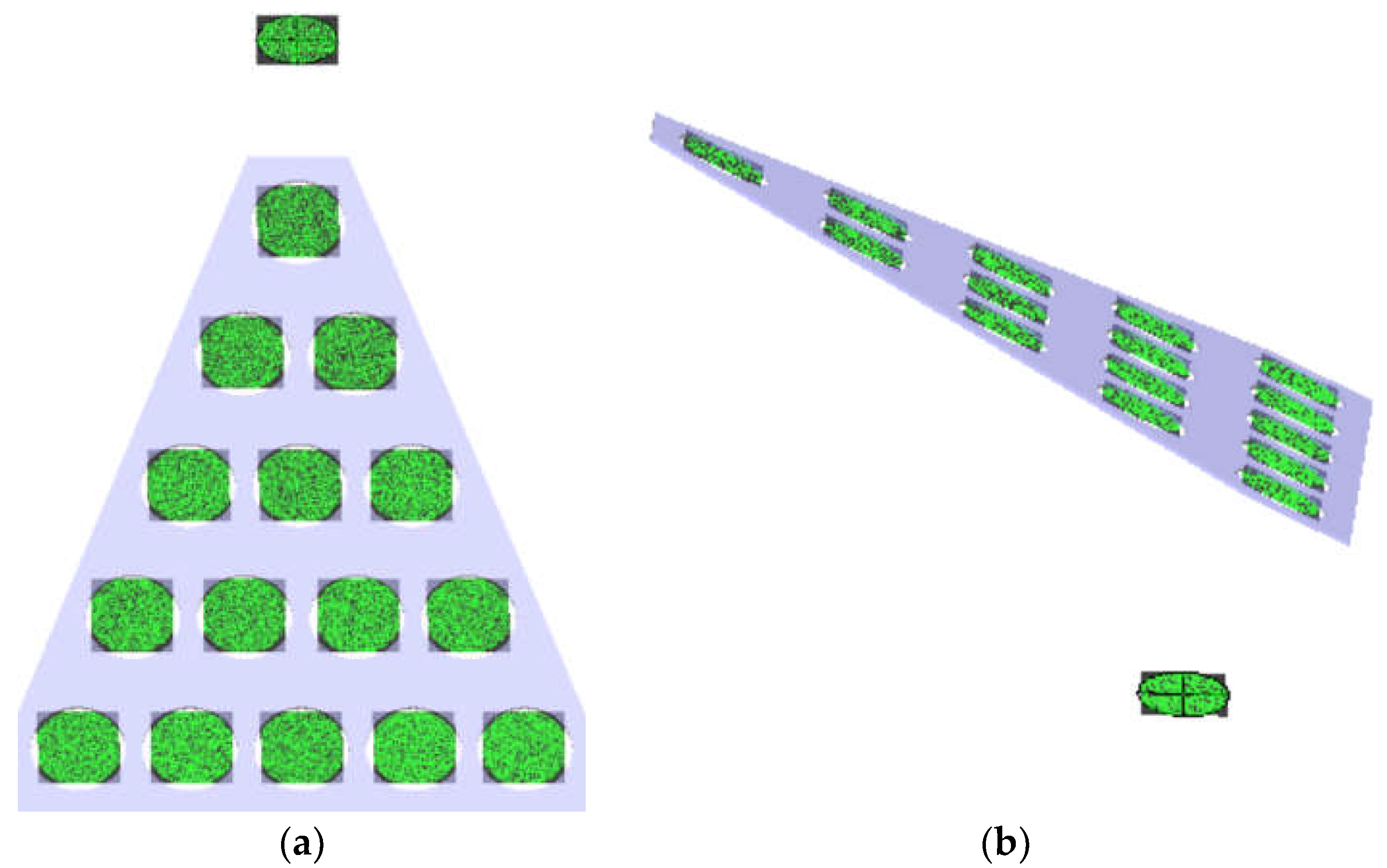
2.6. Optical Characteristics and Optical Constants

The optical transmittance of the samples for different segments is measured by an ultraviolet/visible/NIR spectrometer. By observing the shift of transmission spectrum, we can preliminarily judge whether the thickness distribution of the film is uniform. The optical constants of thin films can be measured by ellipsometric technique [23,24]. In addition to measuring the refractive index and extinction coefficient, we need to further understand whether the film thickness distribution of the films deposited at different locations is uniform An ellipsometer has a semiconductor laser with a wavelength of 656 nm. The ellipsometer includes two polarizers with the angles of 45° and −45°. The double incident angle method with two incident angles of 30° and 60° are used to measure the amorphous oxide films. A laser beam passing through the analyzers and thin film sample, the reflective light intensity was measured by an optical powermeter. The ellipsometric parameters were calculated based on the functional relationship between the light intensity and the polarization angle and the analyzer angle. Then we use the Newton iteration method to calculate the ellipsometric parameters and convert them into optical constants.

3. Result and Discussion

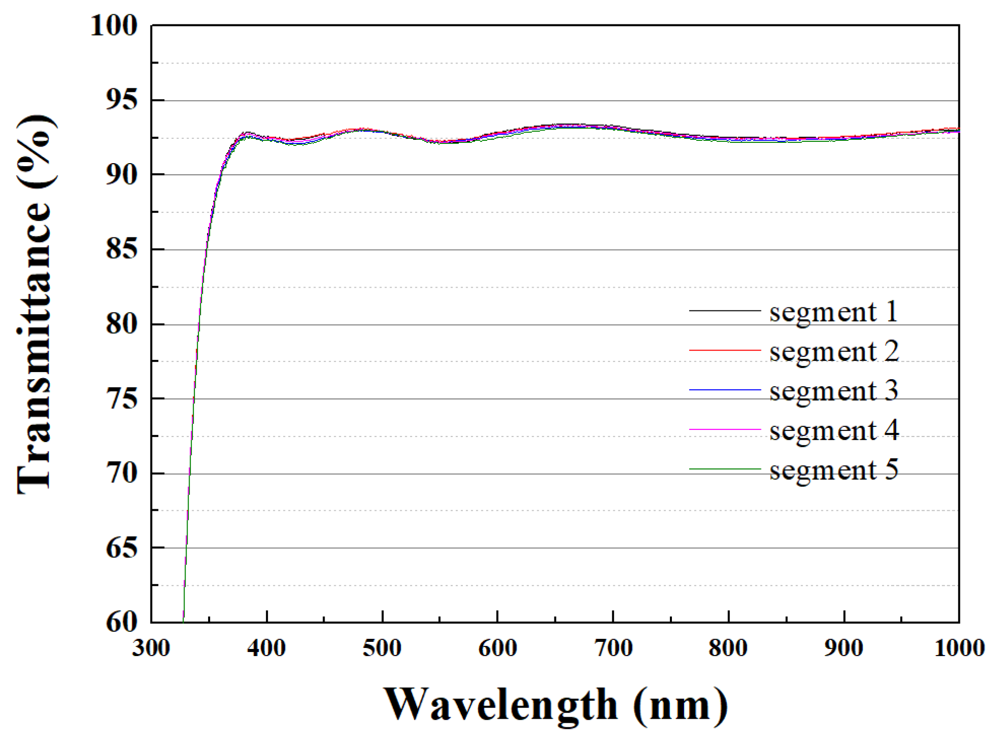
3.1. Optical Constant and Thickness Analysis of SiO2 Thin Film

The transmittance of the SiO2 thin film was measured by the ultraviolet/visible/NIR spectrometer. It can be found that the curves of the transmittance spectrum are almost overlapped, as shown in Figure 6. There is no obvious waveform drift phenomenon, which means that the films deposited in different segments thickness with good consistency. The average transmittance is higher than 90% in the wavelength of 400 to 800 nm. The transmission spectrum with high transmittance shows a good optical performance. The transmission spectrogram is measured from different positions. The peaks and valleys at different positions are very close, and the difference is less than 1%.
The relative relationship between the refractive index and the extinction coefficient can be obtained from the transmittance. The refractive indices of the five different segments are 1.429, 1.437, 1.443, 1.438, and 1.449, as shown in Table 1. The highest refractive index is 1.449 for segment five. The lowest refractive index is 1.429 for segment one. The extinction coefficients of the deposited oxide films at different positions are analyzed. The analyzed extinction coefficients of the five different segments are 0.0007, 0.0007, 0.0004, 0.0005, 0.0006, respectively. The maximum extinction coefficient is 0.0007 for segments one and two. The minimum extinction coefficient is 0.0004 for segment three. The analysis results show that the extinction coefficients are very close. Because the analyzed wavelength is 656 nm, the absorption of the thin film is very small at longer wavelengths, and the SiO2 thin film has a high transmittance.
The surface profiler α-step was used to measure and analyze the film thickness of different segments. The film thicknesses of the five segments is 566.76 nm, 567.58 nm, 566.17 nm, 567.76 nm, and 570.47 nm, respectively. The results show that the film thickness of segment five is the thickest. The film thickness of segment three is the thinnest. The average film thickness of the five segments is 567.74 nm. The thickness different between the thickest and thinnest film is 4.3 nm, so that the uniformity of the film thickness distribution is good. The film thickness of the five different segments is normalized. The thickness uniformity of the SiO2 film can be calculated to be 0.38%. The relative thickness of segments one to five is very close, as shown in Figure 7.

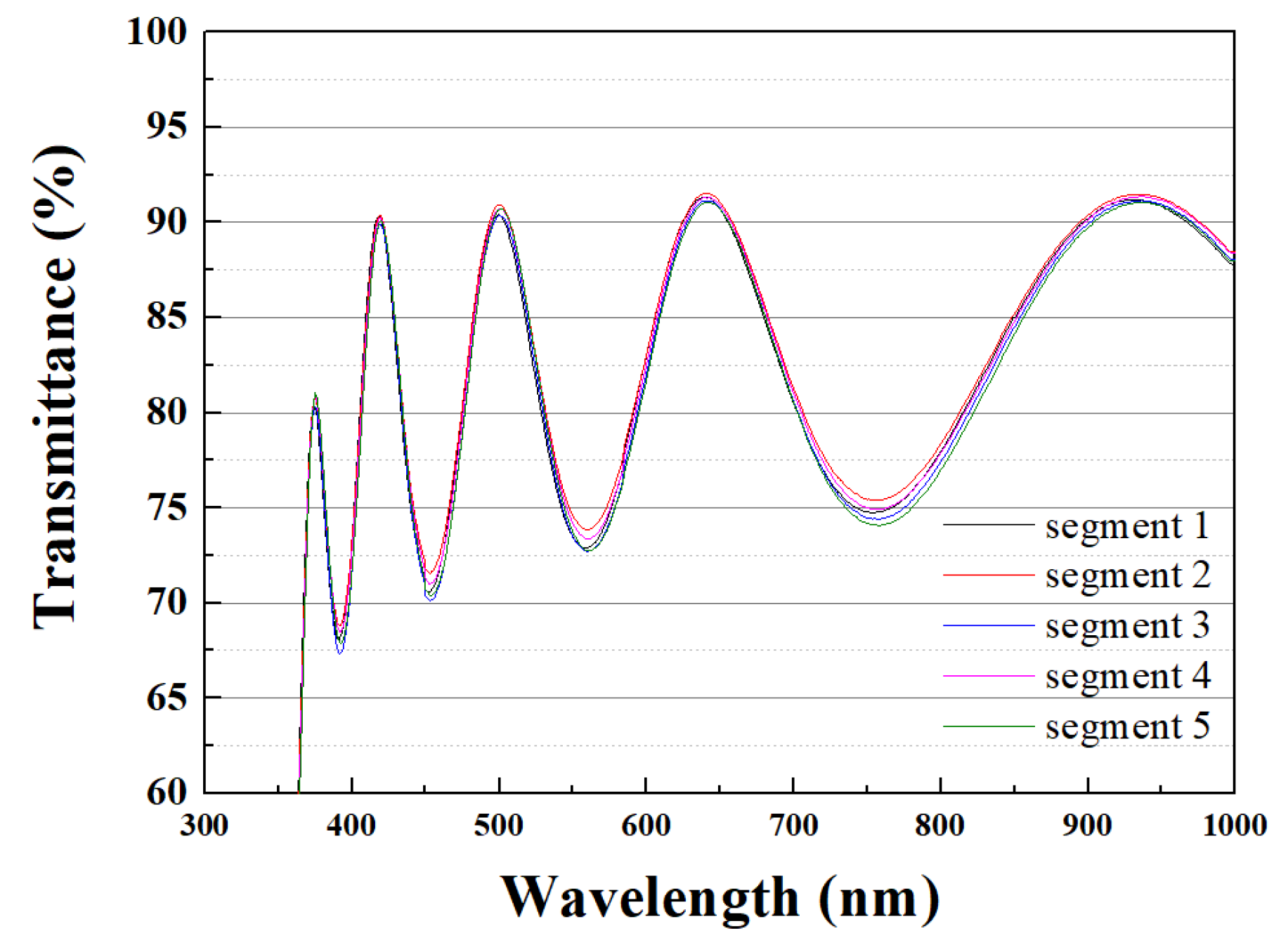
3.2. Optical Constant and Thickness Analysis of Ta2O5 Thin Film

We use an optical spectrophotometer to measure the transmission spectrum of the Ta2O5 thin film. It can be found that the curves of the transmission spectra almost overlap, as shown in Figure 8. There is no obvious waveform drift, which means that the thickness of the film deposited at different positions is uniform. The average transmittance in the wavelength of 400 to 800 nm is higher than 85%, which has a good optical transmittance. But it was found that the transmittance is different, which means that the refractive index or extinction coefficient of different segments will be different. The transmission spectra were measured from different positions of the samples. The transmittance difference is about 1%. The optical constants are determined by an ellipsometer. The refractive indices of the five segments are 2.023, 2.039, 2.045, 2.026, and 2.031, as shown in Table 2. The highest refractive index is 2.045 for the segment three. The lowest refractive index is 2.023 for the segment one. The extinction coefficients of the Ta2O5 thin films for different segments are also analyzed. The analyzed extinction coefficients are 0.004, 0.007, 0.007, 0.004, and 0.003, respectively. The maximum extinction coefficient is 0.007 for the segments two and three. The minimum extinction coefficient is 0.003 for the segment five. The analysis results show that the extinction coefficients are very small, the absorption of the Ta2O5 thin films at longer wavelengths is less than 1 × 10⁻³.
The surface profiler was used to measure and analyze the film thickness of different segments. The film thicknesses of the five segments are 480.38 nm, 480.82 nm, 482.23 nm, 483.86 nm, and 483.53 nm, respectively. The results show that the film thickness of the segment five is the thickest. The film thickness of the segment one is the thinnest. The average thickness of the Ta2O5 thin film at different positions is 483.86 nm. The thickness difference between the thickest and thinnest films was 3.48 nm, so the uniformity of the film thickness distribution was good. If the film thicknesses of the five segments are normalized, the thickness uniformity of the Ta2O5 film can be calculated to be 0.36%, and the relative thicknesses of segments 1 to 5 are close, as shown in Figure 9.

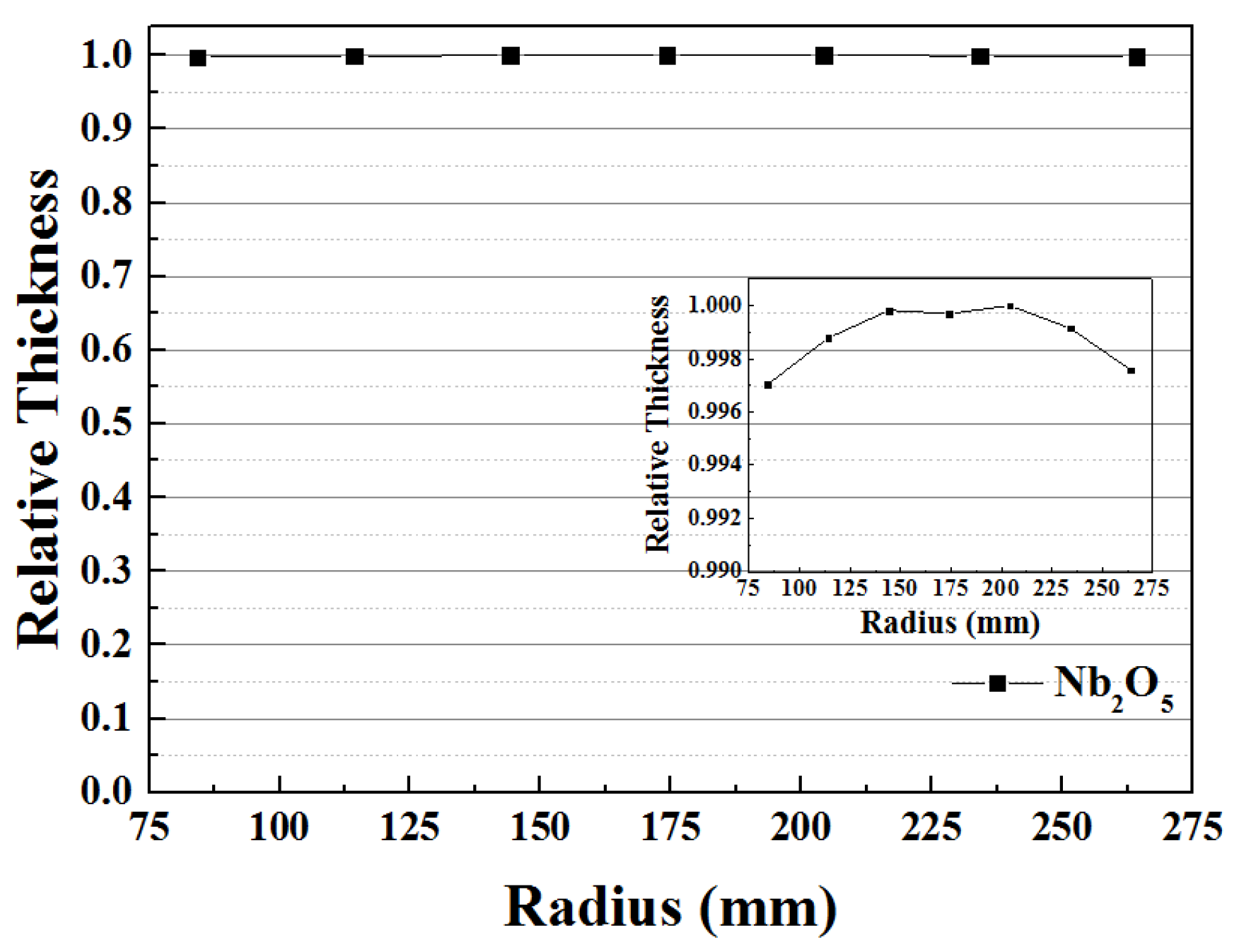
3.3. Optical Constant and Thickness Analysis of Nb2O5 Thin Film

The transmission spectrum of the Nb2O5 thin film was measured by the optical spectrophotometer. It can be seen that the curves of the transmission spectra almost overlap, as shown in Figure 10. There is no obvious waveform shift, which means that the thickness of the thin film deposited at different positions is good. The average transmittance in the wavelength of 400–800 nm is higher than 80%. Transmission spectra were measured from different positions. There was no significant difference in transmittance levels, and the transmittance difference was less than 1%. This result shows that the difference in refractive index or extinction coefficient of the Nb2O5 thin films was not significant.
We measured the optical constants of the Nb2O5 films with an ellipsometer, and the results showed that the refractive indices of the five segments were 2.281, 2.261, 2.284, 2.272, and 2.275, as shown in Table 3. The highest refractive index is 2.261 for segment two. The lowest refractive index is 2.284 for segment three. The extinction coefficients of the Nb2O5 thin films deposited at different positions were also analyzed. The analyzed extinction coefficients were 0.007, 0.009, 0.008, 0.008, and 0.006, respectively. The highest extinction coefficient is 0.009 for the position of segment two. The lowest extinction coefficient is 0.006 for the position of segment five. The analysis results show that the extinction coefficient is small. This suggests that the absorption of the Nb2O5 thin film is smaller at the longer wavelength.
The surface profiler was used to measure and analyze the film thickness of different segments. The film thickness distribution of different segments (from 1 to 5) is 420.86 nm, 421.82 nm, 421.41 nm, 421.93 nm, and 422.17 nm, respectively. The results show that the film thickness of segment 5 is 422.17 nm and its thickness is the thickest. The film thickness of segment one is 420.86 nm and its thickness is the thinnest. The average thickness of the deposited film at five different positions is 421.63 nm. The thickness difference between the thickest and thinnest films is 1.31 nm, so the uniformity of the film thickness distribution is good. If the film thicknesses of the five different segments are normalized, then film thickness uniformity is calculated to be 0.15%. The relative thicknesses of segments 1 to 5 are very close, as shown in Figure 11.

4. Conclusions

In this work, the coating mask width at different segments can be obtained using optical simulation combined with flux mapping method. The dimensions of the coating mask can be precisely obtained, which can increase the thickness uniformity of the different segments. From the analysis results of different oxide films, it can be seen that the uniformity is less than 0.4%. A good uniform film thickness distribution can be obtained by electron beam evaporation with IAD technique. The thickness uniformity is 0.38% for SiO2 film, 0.36% for Ta2O5 film, and 0.15% for Nb2O5 film, respectively. The results show that Nb2O5 film has the best thickness uniformity. We also solved the problem of the thinner film thickness in the area farthest from the evaporation source. For the optical performance, the average transmittance of the SiO2 film in the visible light band is higher than 90%. The average transmittance of the Ta2O5 film is higher than 85%. The average transmittance of the Nb2O5 film is higher than 80%. In addition, the extinction coefficients of the three oxide films are small, and their values are in the order of 10−3. These results show that three kinds of amorphous thin films have good optical properties. These results show that the three kinds of amorphous films have good optical properties, which is helpful to develop new thin-film components.

Author Contributions

Conceptualization and methodology, C.-L.T.; writing—review and editing, C.-L.T.; validation, C.-L.T. and K.-S.C.; software, K.-S.C.; data curation, K.-S.C. All authors have read and agreed to the published version of the manuscript.

Funding

This research was supported in part by the National Science and Technology of Council, under project number 111-2622-E-035-003.

Institutional Review Board Statement

Not applicable.

Informed Consent Statement

Not applicable.

Data Availability Statement

Not applicable.

Conflicts of Interest

The authors declare no conflict of interest.

References

  1. Fancey, K.S. A coating thickness uniformity model for physical vapor-deposition systems: Overview. Surf. Coat. Technol. 1995, 71, 16–29. [Google Scholar] [CrossRef]
  2. Swann, S.; Collett, S.A.; Scarlett, I.R. Film thickness distribution control with off-axis circular magnetron sources onto rotating substrate holders: Comparison of computer simulation with practical results. J. Vac. Sci. Technol. A 1990, 8, 1299–1303. [Google Scholar] [CrossRef]
  3. Ho, C.Y.; Chen, B.C.; Xiong, C.W.; Fan, S.L.; Wan, S.F.; Li, L.G.; Shu, Y.F.; Yu, X.Q. A novel spatial-distribution-function of electron beam-induced vapor plume for analyzing EBPVD thickness. AIP Adv. 2018, 8, 085108. [Google Scholar] [CrossRef] [Green Version]
  4. Villa, F.; Martínez, A.; Regalado, L.E. Correction masks for thickness uniformity in large-area thin films. Appl. Opt. 2000, 39, 1602–1610. [Google Scholar] [CrossRef]
  5. Wang, B.; Fu, X.; Song, S.; Chu, H.O.; Gibson, D.; Li, C.; Shi, Y.; Wu, Z. Simulation and Optimization of Film Thickness Uniformity in Physical Vapor Deposition. Coatings 2018, 8, 325. [Google Scholar] [CrossRef] [Green Version]
  6. Savale, P.A. Physical vapor deposition (PVD) methods for synthesis of thin films: A comparative study. Arch. Appl. Sci. Res. 2016, 8, 1–8. [Google Scholar]
  7. Pinard, L.; Michel, C.; Sassolas, B.; Balzarini, L.; Degallaix, J.; Dolique, V.; Flaminio, R.; Forest, D.; Granata, M.; Lagrange, B.; et al. The mirrors used in the LIGO interferometers for the first-time detection of gravitational waves. Appl. Opt. 2017, 56, C11–C15. [Google Scholar] [CrossRef] [Green Version]
  8. Raut, H.K.; Ganesh, V.A.; Nair, A.S.; Ramakrishna, S. Anti-reflective coatings: A critical, in-depth review. Energy Environ. Sci. 2011, 4, 3779–3804. [Google Scholar] [CrossRef]
  9. Lee, C.C. Thin Film Optics and Coating Technology; Yi Hsien Publishing Co., Ltd.: Taipei, China, 2019. [Google Scholar]
  10. Gross, M.; Dligatch, S.; Chtanov, A. Optimization of coating uniformity in an ion beam sputtering system using a modified planetary rotation method. Appl. Opt. 2011, 50, C316–C320. [Google Scholar] [CrossRef]
  11. Kozlovskiy, A.L.; Zdorovets, M.V. Synthesis, structural, strength and corrosion properties of thin films of the type CuX (X = Bi, Mg, Ni). J. Mater. Sci. Mater. Electron. 2019, 30, 11819–11832. [Google Scholar] [CrossRef]
  12. Zubar, T.I.; Usovich, T.I.; Tishkevich, D.I.; Kanafyev, O.D.; Fedkin, V.A.; Kotelnikova, A.N.; Panasyuk, M.I.; Kurochka, A.S.; Nuriev, A.V.; Idris, A.M.; et al. Features of Galvanostatic Electrodeposition of NiFe Films with Composition Gradient: Influence of Substrate Characteristics. Nanomaterials 2022, 12, 2926. [Google Scholar] [CrossRef]
  13. Kadyrzhanov, K.K.; Shlimas, D.I.; Kozlovskiy, A.L.; Zdorovets, M.V. Research of the shielding effect and radiation resistance of composite CuBi2O4 films as well as their practical applications. J. Mater. Sci. Mater. Electron. 2020, 31, 11729–11740. [Google Scholar] [CrossRef]
  14. Trukhanov, A.V.; Grabchikov, S.S.; Solobai, A.A.; Tishkevich, D.I.; Trukhanov, S.V.; Trukhanova, E.L. AC and DC-shielding properties for the Ni80Fe20/Cu film structures. J. Magn. Magn. Mater. 2017, 443, 142–148. [Google Scholar] [CrossRef]
  15. Trukhanov, S.V.; Trukhanov, A.V.; Vasiliev, A.N.; Szymczak, H. Frustrated exchange interactions formation at low temperatures and high hydrostatic pressures in La0.70Sr0.30MnO2.85. J. Exp. Theor. Phys. 2010, 111, 209–214. [Google Scholar] [CrossRef]
  16. Zhumatayeva, I.Z.; Kenzhina, I.E.; Kozlovskiy, A.L.; Zdorovets, M.V. The study of the prospects for the use of Li0.15Sr0.85TiO3 ceramics. J. Mater. Sci. Mater. Electron. 2020, 31, 6764–6772. [Google Scholar] [CrossRef]
  17. Ghiyasiyan-Arani, M.; Salavati-Niasari, M. New nanocomposites based on Li-Fe-Mn double spinel and carbon self-doped graphitic carbon nitrides with synergistic effect for electrochemical hydrogen storage application. Ind. Eng. Chem. Res. 2019, 58, 23057–23067. [Google Scholar] [CrossRef]
  18. Ghiyasiyan-Arani, M.; Salavati-Niasari, M.; Zonouz, A.F. Effect of operational synthesis parameters on the morphology and the electrochemical properties of 3D hierarchical AlV3O9 architectures for Li-Ion batteries. J. Electrochem. Soc. 2020, 167, 020544. [Google Scholar] [CrossRef]
  19. Ghiyasiyan-Arani, M.; Masoud Salavati-Niasari, M. Strategic design and electrochemical behaviors of Li-ion battery cathode nanocomposite materials based on AlV3O9 with carbon nanostructures. Compos. Part B 2020, 183, 107734. [Google Scholar] [CrossRef]
  20. Kim, M.G.; Pahk, H.J. Simulation of thin film thickness distribution for thermal evaporation process using a scanning linear source. J. SID 2017, 25, 249–257. [Google Scholar] [CrossRef]
  21. Burkhard, D.G.; Shealy, D.L. Flux density for ray propagation in geometrical optics. J. Opt. Soc. Am. 1973, 63, 299–304. [Google Scholar] [CrossRef]
  22. Mao, X.; Li, H.; Han, Y.; Luo, Y. Polar-grids based source-target mapping construction method for designing freeform illumination system for a lighting target with arbitrary shape. Opt. Express 2015, 23, 4313–4328. [Google Scholar] [CrossRef]
  23. Tang, C.J.; Chang, R.S.; Han, C.Y. Using imaging ellipsometry to determine angular distribution of ellipsometric parameters without scanning mechanism. Opt. Lasers Eng. 2016, 77, 39–43. [Google Scholar] [CrossRef]
  24. Vuye, G.; López-Ríos, T. Precision in the ellipsometric determination of the optical constants of very thin films. Appl. Opt. 1982, 21, 2968–2971. [Google Scholar] [CrossRef]
Figure 1. Flow chart of film thickness uniformity simulation for the coating experiment.
Applsci 12 11878 g001
Figure 2. The geometric position distribution of the evaporation coater, including electron gun, ion assisted deposition (IAD), quartz monitoring sensor, optical monitoring system, mask and the coating substrate holder.
Applsci 12 11878 g002
Figure 3. Ray tracing considers the electron beam evaporation source as a similar point light source with a divergence angle of 60 degrees.
Applsci 12 11878 g003
Figure 4. Geometric positions of optical monitoring and quartz monitoring systems (a) An optical monitoring component and coating substrate holder; (b) A quartz monitoring sensor and coating substrate holder (served as a receiver).
Applsci 12 11878 g004
Figure 5. Film thickness distribution curve for different segments from one to five.
Applsci 12 11878 g005
Figure 6. Transmission spectra of SiO2 thin film deposited on different segments from one to five.
Applsci 12 11878 g006
Figure 7. Relative thickness of SiO2 thin film deposited on a large substrate with a radius of 275 mm.
Applsci 12 11878 g007
Figure 8. Transmission spectra of Ta2O5 thin film deposited on different segments.
Applsci 12 11878 g008
Figure 9. Relative thickness of Ta2O5 thin film deposited on a large substrate with a radius of 275 mm.
Applsci 12 11878 g009
Figure 10. Transmission spectra of Nb2O5 thin film deposited on different segments.
Applsci 12 11878 g010
Figure 11. Relative thickness of Nb2O5 thin film deposited on a large substrate with a radius of 275 mm.
Applsci 12 11878 g011
Table 1. Optical constants of SiO2 thin films with different segments.
SegmentRefractive IndexExtinction CoefficientFilm Thickness (nm)
One1.4290.0007566.76 nm
Two1.4370.0007567.58 nm
Three1.4430.0004566.17 nm
Four1.4380.0005567.76 nm
Five1.4490.0006570.47 nm
Table 2. Optical constants of Ta2O5 thin film for different segments.
SegmentRefractive IndexExtinction CoefficientFilm Thickness (nm)
One2.0230.004480.38 nm
Two2.0390.007480.82 nm
Three2.0450.007482.23 nm
Four2.0260.004483.86 nm
Five2.0310.003483.53 nm
Table 3. Optical constants of Nb2O5 thin film with different segments.
SegmentRefractive IndexExtinction CoefficientFilm Thickness (nm)
One2.2810.007420.86 nm
Two2.2610.009421.82 nm
Three2.2840.008421.41 nm
Four2.2720.008421.93 nm
Five2.2750.006422.17 nm
Publisher’s Note: MDPI stays neutral with regard to jurisdictional claims in published maps and institutional affiliations.

