Article

Thermal Stability of Self-Assembled 3-Aminopropyltrimethoxysilane Diffusion Barrier Terminated by Carboxyl Groups

1
College of Material Science and Chemical Engineering, Harbin Engineering University, Harbin 150001, China
2
Key Laboratory of Superlight Material and Surface Technology, Ministry of Education, Harbin Engineering University, Harbin 150001, China
3
Institute of Surface Science and Technology, Harbin Engineering University, Harbin 150001, China
*
Author to whom correspondence should be addressed.
Appl. Sci. 2022, 12(21), 11098; https://doi.org/10.3390/app122111098
Submission received: 6 October 2022 / Revised: 29 October 2022 / Accepted: 31 October 2022 / Published: 2 November 2022
(This article belongs to the Special Issue Micro- and Nanomanufacturing: From Nanoscale Structures to Devices)

Abstract

:
The carboxyl-terminated 3-aminopropyltrimethoxysilane (APTMS) self-assembled monolayer (SAM) diffusion barrier was prepared onto a Si substrate via molecular self-assembly and graft modification technology. The SAM was afterward coated with a copper film via radio-frequency (RF) magnetron sputtering. In order to study the thermal stability of the diffusion barrier, the sample was subsequently annealed for 60 min in an Ar environment at the temperatures of 350 °C, 400 °C, 450 °C, 500 °C, and 550 °C. The results revealed that carboxyl modification enabled one to increase the barrier breakdown temperature of the APTMS diffusion barrier layer by about 100 °C, which was sufficient to effectively inhibit the copper diffusion at 500 °C.

1. Introduction

With the rapid development of the semiconductor industry in the past decades, aluminium wire materials have gradually been replaced with Cu in integrated circuit interconnects because of its good electrical conductivity and electromigration resistance [1]. However, Cu has a high diffusivity, which results in the easy diffusion between Cu and Si/SiO2 layers [2], causing defects and affecting the service life of carriers as well as deteriorating the performance of the electronic components [3,4,5]. In order to solve the problems associated with copper diffusion and to enhance the bonding force between the copper and dielectric components, a diffusion barrier layer was introduced between the Cu and Si/SiO2 layers [6,7,8,9,10]. The earlier diffusion barriers mainly included transition metals (Ti [11], Ta [12], W [13]) along with related binary (TaN [12], ZrSi [14], TiN [15]) and ternary (Zr-Ti-Ni [16], W-B-N [17]) compounds. Meanwhile, the above-mentioned diffusion barriers cannot completely cover the surface of the device in the groove with a large depth ratio, which decreases the continuity of the copper film. In addition, most barriers are mainly prepared via magnetron sputtering, which imposes limits on their minimum thickness to 5 nm. Thus, the fabrication of diffusion barriers with good thermal stability, perfect coverage, and ultra-small thickness for copper interconnections and their large-scale application in the new generation of Si integration technology are urgent tasks.
In recent years, self-assembly technology has aroused considerable attention among researchers [18] as a promising method for preparing 3-aminopropyltrimethoxysilane (APTMS) diffusion barriers for Cu metallization systems [19,20,21,22,23,24,25,26,27]. The organosilane is first hydrolyzed and adsorbed on the treated silicon substrate and then dehydrated to form a Si-O-Si bond, whereas the other end of -NH2 can be well bonded to copper. Compared with -NH2, the -COOH groups can better fix copper and prevent copper diffusion [28].
In view of the above, a chemically modified APTMS is proposed in this study to enhance the diffusion barrier properties and the adhesion between the APTMS and the copper film. Trimesic acid is chosen as a modifying molecule for the APTMS. According to the results, the presence of benzene rings in trimesic acid enables one to enhance the properties of the diffusion barrier. In addition, two active sites in the -COOH groups ensure better bonding between the barrier and the copper film.

2. Experimental

2.1. Samples Preparation

P-type Si (100) wafers (Ningbo Saibang International Trade Co., Ltd., Ningbo, China) were used as the substrates. They were degreased using ultrasonic agitation in acetone and deionized water sequentially then cleaned with a concentrated H2SO4: 30% H2O2 (4:1, v/v) solution for 10 min at 120 °C. The substrates were dipped in a 30% ammonia water: 30% H2O2:H2O (1:1:5, v/v) solution for 10 min at 85 °C and finally cleaned with a concentrated HCl: 30% H2O2:H2O (1:1:6, v/v) solution for 10 min at 85 °C. After each cleaning step, the silicon substrates were rinsed at least three times with deionized water. Finally, the substrates were blow-dried with nitrogen. This enabled one to obtain a thin silicon dioxide film on the surface of each silicon substrate [29].
After that, each Si substrate with a film was immersed in a 3 mmol/L toluene solvent to prepare an APTMS structure. The samples were then washed with toluene and ethanol and finally dried with N2. The trimesic acid solution was prepared using 3 mmol/L pyridine as a solvent and silicon tetrachloride as a dehydrating agent, and the silicon wafers with a self-assembled APTMS were immersed in it for 1 h to 4 h. The reaction temperature was 70 °C. Finally, the samples were washed with ethanol and blow-dried with nitrogen.
The copper films were afterward deposited onto the COOH-APTMS diffusion barriers in a pure Ar environment via RF magnetron sputtering under a working pressure of 0.3 Pa. The sputtering power was 100 W and the sputtering time was 5 min. Finally, the Cu/COOH-APTMS/SiO2/Si samples were annealed for 60 min in an Ar medium at 350 °C, 400 °C, 450 °C, 500 °C, and 550 °C.

2.2. Analytical Methods

The contact angles of the films (CAs) were measured with a CA system (Model OCA100, Dataphysics, Stuttgart, Germany). Each time, a pure water drop was placed on the surface of the tested sample. After the drop was balanced, the instrument’s own software was used to calculate the contact angle. Five different areas were selected on each sample surface for water contact angle measurements, and the average contact angle was determined.
X-ray photoelectron spectroscopy (XPS) (Model Escalab Xi+, Thermo Fisher Scientific, Waltham, MA, USA) was employed to distinguish between the chemical states of the elements in the top surface layer. The XPS analysis was performed using a monochromatic Al Kα X-ray source within the O1s, N1s, C1s, and Si2p spectral ranges. The binding energy positions of the peaks were adjusted by setting the C1s peak to 284.8 eV.
The surface morphology of the samples was examined via scanning electron microscopy (SEM) (Model Thermo Scientific Apreo S, Thermo Fisher Scientific, USA) under high-vacuum conditions and the operating voltage of 5 kV. Prior to the measurements, a gold layer was spray-deposited on each sample surface.
The surface roughness of the samples was assessed by atomic force microscopy (AFM) (Model Dimension Icon, Bruker, Ettlingen, Germany) within a surface area of 1 μm ×1 μm. The Scanasyst-air probe model and Scan Asyst test mode were used in testing, and the elastic constant of the probe was 0.4 N/m. The roughness tests were performed within five areas on each sample surface, and the root-mean-square roughness (RMS) values were obtained by averaging the data.
The phase analysis of the samples before and after heat treatment was conducted via X-ray diffraction (XRD) (Model X’Pert Pro, PANalytical B.V., Almelo, The Netherlands) at the tube voltage of 40 kV, tube current of 40 mA, and 2θ step length of 0.05°. The X-ray radiation source was Cu.
To further evaluate the adhesive performance of the specimens, four-point bending (FPB) tests were implemented by means of an electronic tensile testing machine (Model Instron5569, Instron, Norwood, MA, USA) [30]. In particular, the critical load values were established from the acquired load-displacement curves to calculate the interfacial toughness [31,32]. The formula is as follows [18,30]:
G = K(1 − v2)Pc/E
where E is the elastic coefficient of the substrate; v is the Poisson’s ratio; K is the coefficient, related to the thickness and the geometry of the substrate; and Pc is the critical load value for device fracture.
To evaluate the thermal stability of the films, four-point probe testing (FPP) was conducted using a double-electric four-probe tester (Model RTS-9, GuangZhou 4 probes tech, China). During testing, the change in the resistance of the samples was determined under heat treatment by defining the variation in sheet resistance (Rc) as follows [33]:
Rc = RaRd/Rd
where Ra and Rd are the sheet resistances of the annealed and as-deposited samples, respectively.

3. Results and Discussion

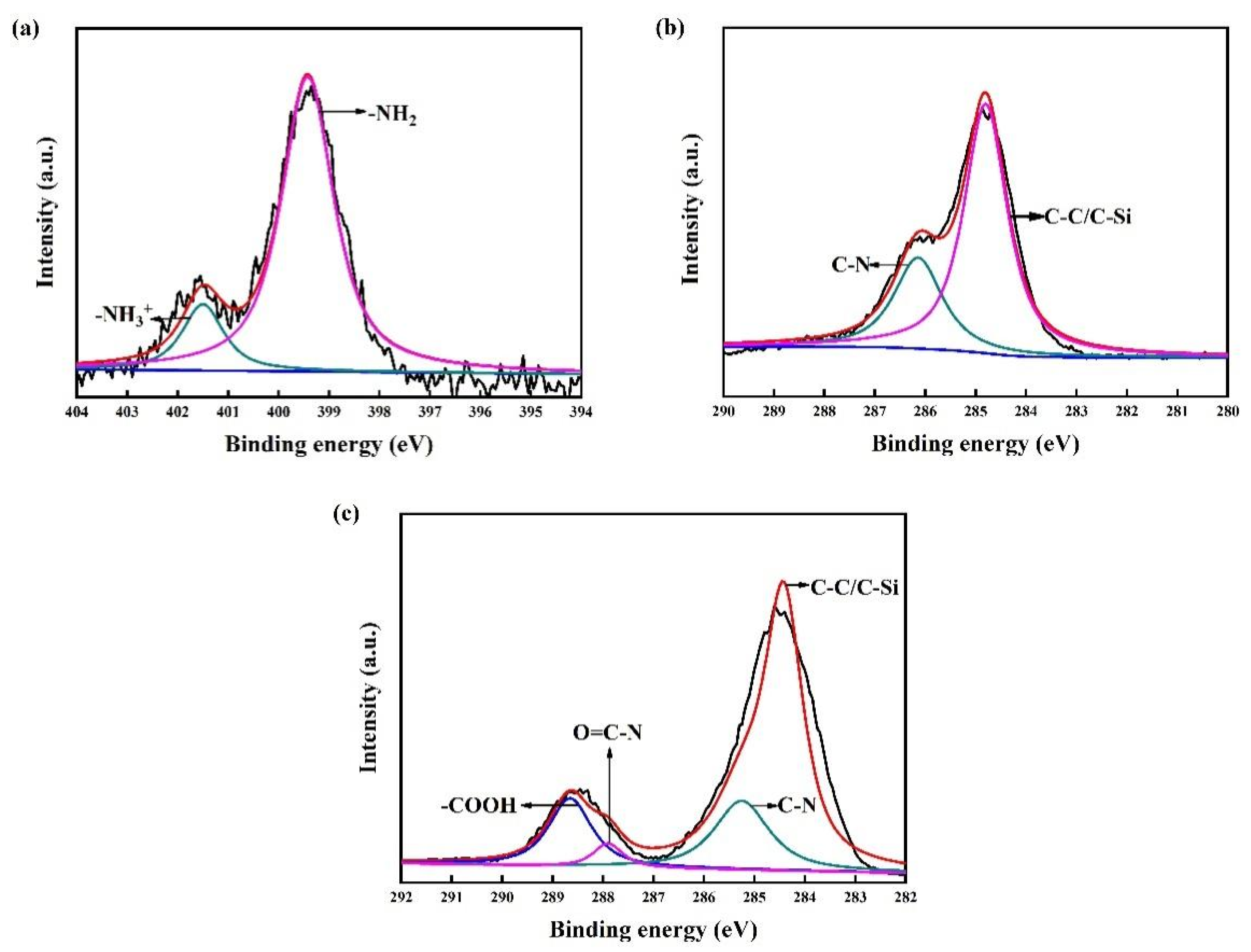
3.1. Characterization of COOH-APTMS SAM

An amino-terminated APTMS-SAM is the basis for carboxyl modification in the preparation of a COOH-APTMS structure. Therefore, the first step of this study was to verify whether the APTMS-SAM system was properly formed. For this purpose, the water contact angles and the XPS data of the APTMS-SAM specimens (Figure 1a) were analysed. According to the results, the water contact angle of the APTMS-SAM was 64.6° ± 2°, and the binding energies of the N1s peaks were 399.7 eV and 401.7 eV. These values were in good agreement with those reported in the literature, [28,34,35] which indicated the successful formation of the APTMS-SAM structure.
Figure 2 displays the SEM images of the COOH-APTMS/SiO2/Si samples at different modification times. At the reaction times of 1 h and 2 h, the unreacted areas were observed on the sample surface (Figure 2a,b) because of the insufficient dehydration condensation reaction between the -NH2 and the -COOH groups. As the reaction time was increased to 3 h, the unreacted areas disappeared, and no obvious particles existed on the surface (Figure 2c). However, after 4 h of the reaction, particles emerged on the surface of the samples (Figure 2d). Those were the partially unreacted trimesic acid residues that remained on the sample surface, while the -NH2 binding sites on the surface were completely reacted. Thus, it could be concluded from the SEM images that the COOH-APTMS SAM structure was successfully assembled, and no particles were detected on the film surface after 3 h of the reaction due to the complete reaction between the APTMS and the trimesic acid.
Figure 3 depicts the AFM images of the COOH-APTMS/SiO2/Si systems at different modification times. From these images, the surface roughness (RMS) for each COOH-APTMS SAM sample was found to be 0.647 nm, 0.907 nm, 1.211 nm, and 1.272 nm, corresponding to the modification times of 1 h, 2 h, 3 h, and 4 h, respectively. Obviously, the RMS value of the COOH-APTMS SAM increased with the increase in the reaction time. The increase in RMS was most pronounced between 1 h and 3 h of the reaction, whereas it was slower after 3 h of modification. In the first case, the remarkable increase in RMS could be explained by the introduction of benzene and carboxyl groups and the extension of the COOH-APTMS chains during the modification process [23,32]. However, the reaction between the APTMS and the trimesic acid after more than 3 h was complete, resulting in a slight change in RMS from 1.211 nm to 1.272 nm due to the accumulation of trimesic acid molecules on the sample surface, which could be observed in the SEM image (Figure 2d).
Figure 1 displays the XPS patterns of the samples. In Figure 1c, the O=C-N-related peak was observed at the binding energy of 287.9 eV. This peak indicated that the carboxyl groups of the trimellitic acid were dehydrated and condensed with the amino groups of the APTMS to form O=C-N bonds [32,36]. Compared to Figure 1b, it could be proved that the trimellitic acid was successfully grafted onto the APTMS surface. In addition, the surface water contact angle of the COOH-APTMS was 35.5° ± 2°, which further confirmed the successful preparation of the COOH-APTMS structure [37].

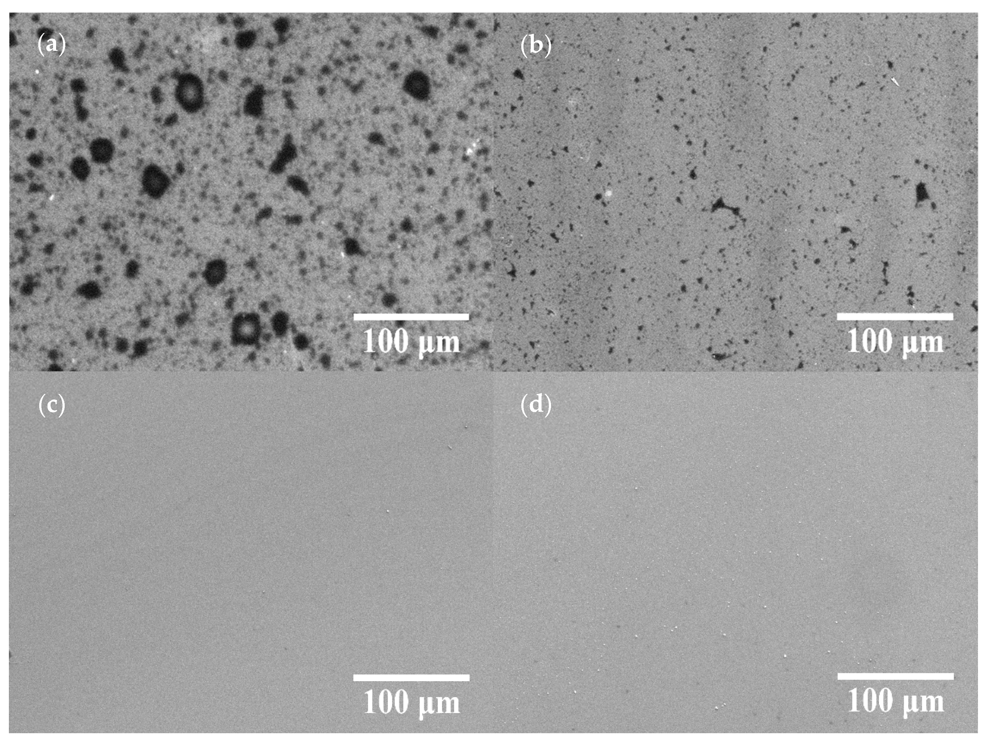
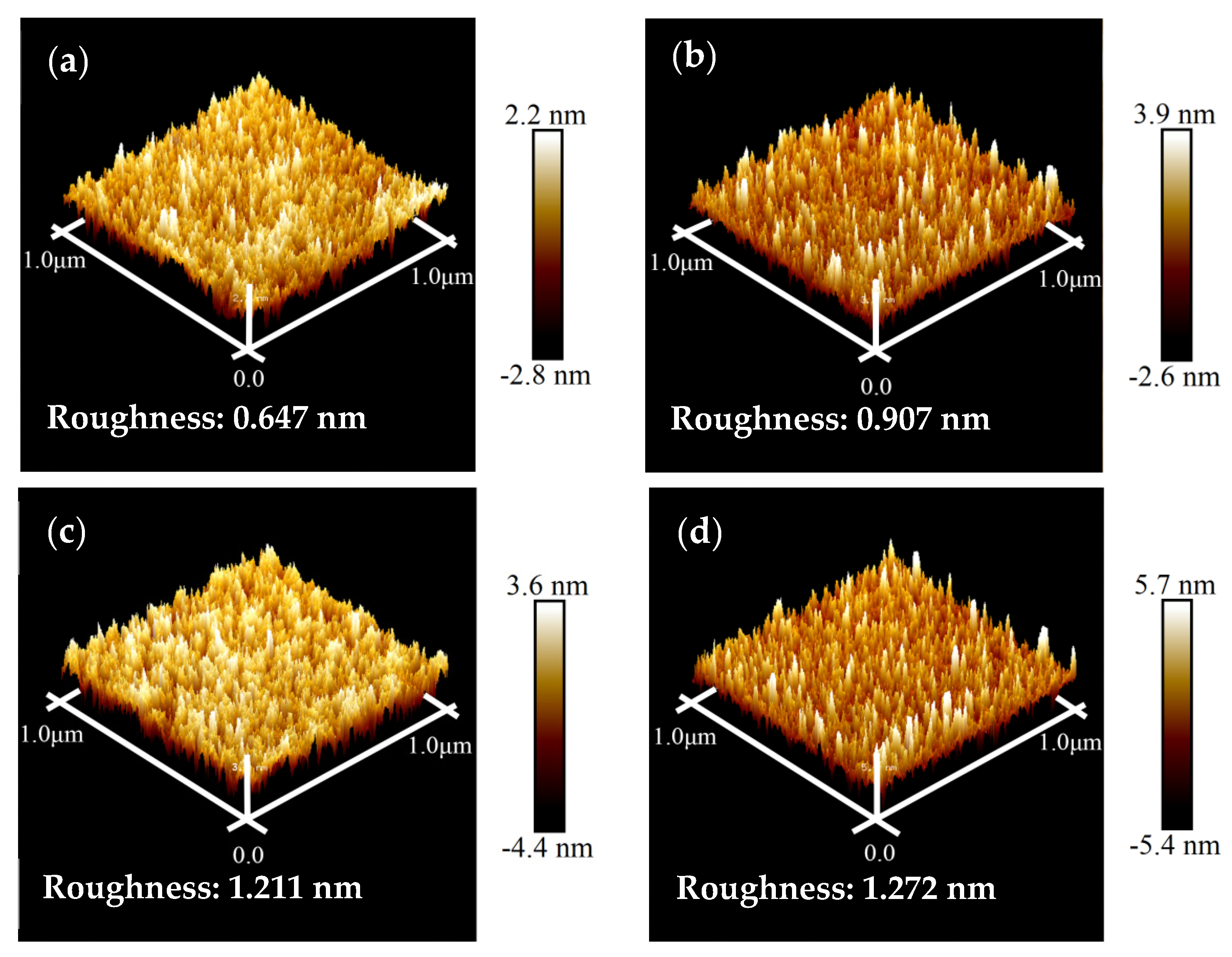
3.2. Combination of Copper Film and COOH-APTMS SAM

To investigate the combination of copper film and a COOH-APTMS SAM, the phase components of the samples were afterward analysed via XPS and XRD (Figure 4). The oxide layer was peeled on the sample surface before the XPS test. In Figure 4a, the characteristic peak of the Cu-O bonds at 933.4 eV meant that there was a strong interaction between the copper atoms and the -COOH groups. In a word, the Cu-O bonds enabled one to fix the copper atoms, which could improve the barrier performance of the COOH-APTMS SAM. The analysis results of the C1s and N1s of the Cu/COOH-APTMS/SiO2/Si samples showed that neither C nor N did not bond with Cu (Figure 4b,c), which was consistent with the literature report [38]. In Figure 4d, the XRD profile exhibited the presence of the Cu phase, while no diffraction peaks of copper oxides were found.
FPB is a reliable method to measure the interfacial adhesion in thin film structures [30,39]. In this study, the interfacial toughness between the copper film and the COOH-APTMS SAM was evaluated before and after annealing at 400 °C to verify the applicability of the semiconductor devices under consideration. Figure 5 depicts the FPB results for different samples. In particular, the interfacial toughness of the modified samples increased significantly compared to that of the Cu/APTMS/SiO2/Si structure, which could be attributed to the good fixation of the Cu film on the APTMS by the forming of Cu-O bonds. After annealing at 400 °C, the dehydration condensation of COOH-APTMS and hydroxyl on the surface of SiO2 was strengthened. Therefore, the interfacial toughness of the Cu/COOH-APTMS/SiO2/Si system increased from 6.58 J/m2 to 7.88 J/m2 (Table 1), which was 19.7% higher than that of the Cu/APTMS/SiO2/Si structure. Thus, the bonding improvement enabled one to better fix the Cu atoms and improve the barrier performance of the diffusion barrier layer.

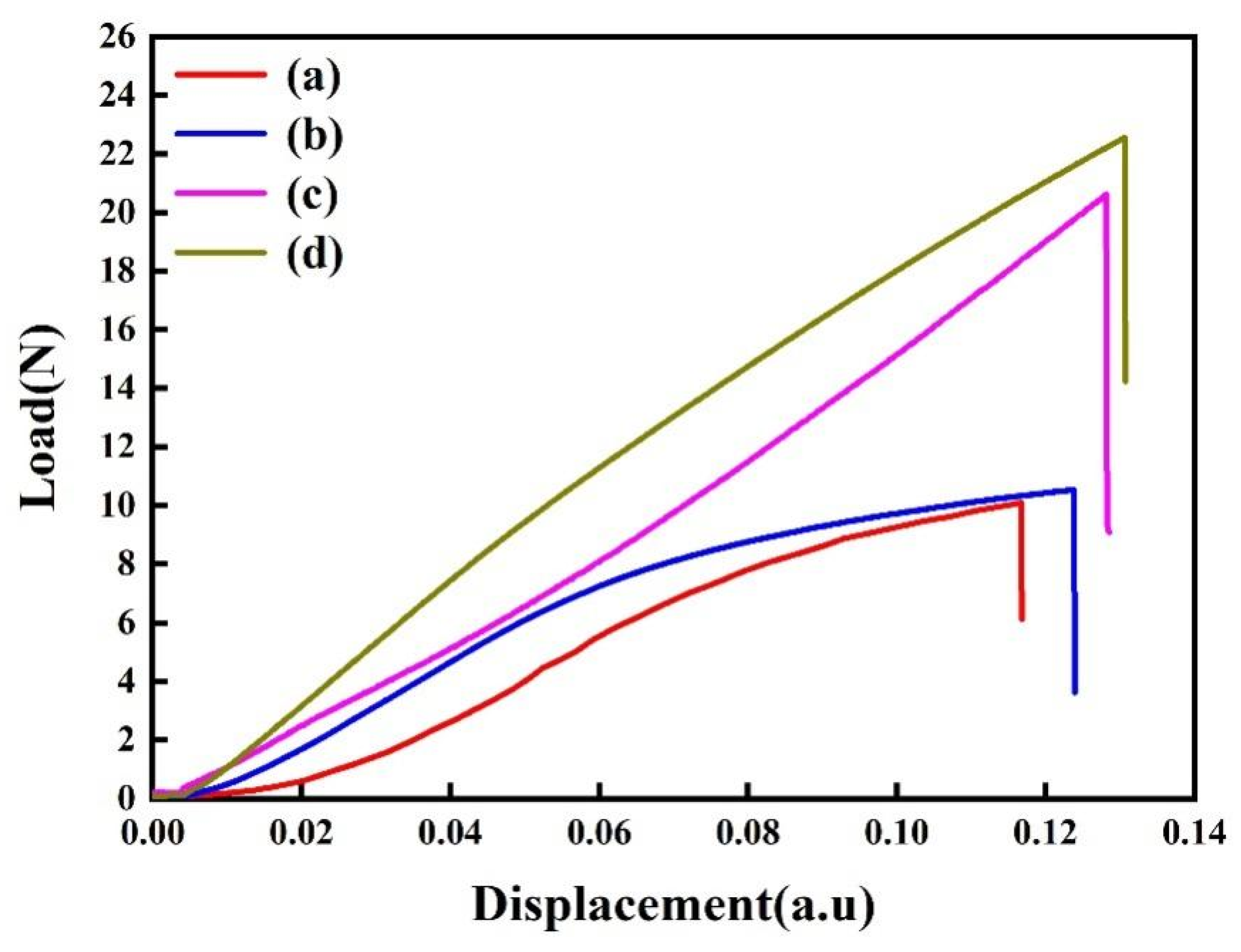
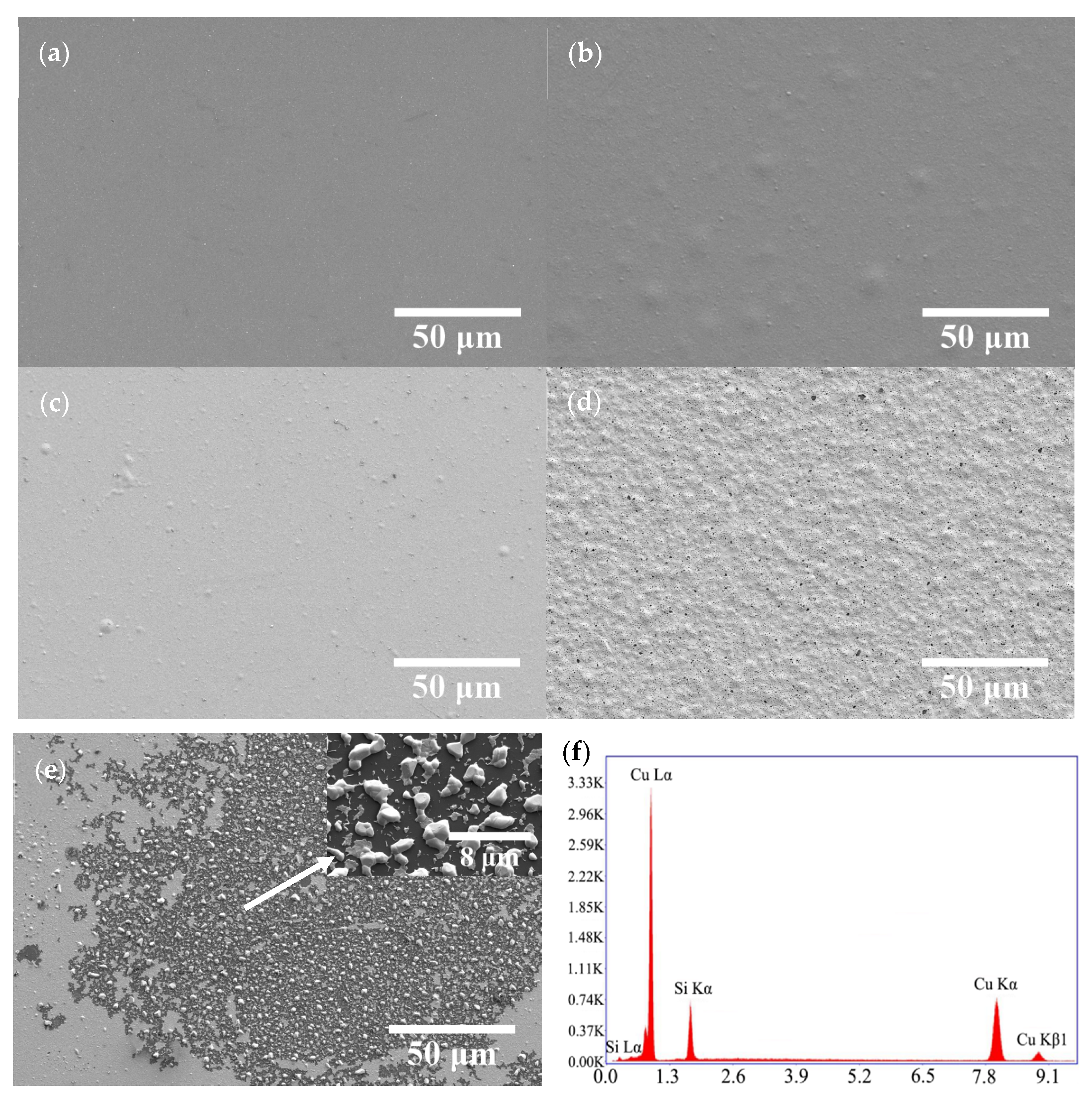
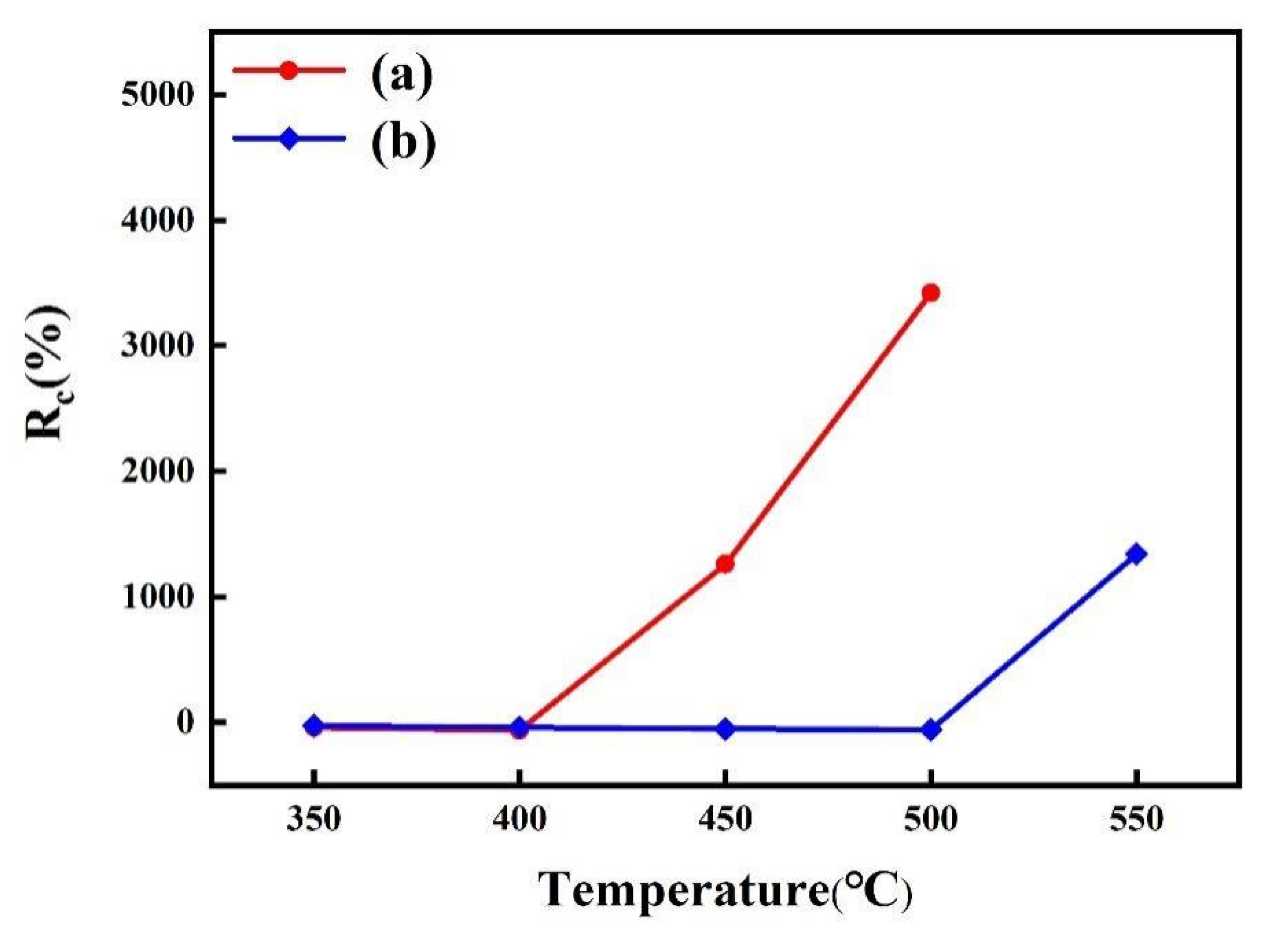
3.3. Thermal Stability of COOH-APTMS SAM

Figure 6 depicts the XRD patterns of the samples after annealing at different temperatures. According to JCPDS no. 96-900-8469, the XRD profiles of the specimens annealed at temperatures below 500 °C revealed only the reflexes of copper, which indicated that the COOH-APTMS diffusion barrier could prevent the copper diffusion up to 500 °C. As the annealing temperature reached 550 °C, a (300) diffraction peak was detected at the position 2θ of 45.00°, which was attributed to a Cu3Si phase (JCPDS no. 00-051-0916). This indicated that the COOH-APTMS diffusion barrier began to fail, losing its diffusion barrier performance at 550 °C. Before and after annealing the Cu/COOH-APTMS/SiO2/Si samples below 500 °C, the Cu (111) diffraction peak was stronger than the Cu (200) one, which meant that the Cu film possessed a (111) preferred orientation. According to the report, [40] a (111) textured Cu film could ensure a higher electromigration resistance.
Figure 7 displays the SEM images of the annealed Cu/COOH-APTMS/SiO2/Si samples. It was evident that the morphology of the copper film was dependent on the annealing temperature. When the temperature was lower than 400 °C, the copper film remained flat (Figure 7a). In turn, at the temperatures above 400 °C, there were some protrusions on the film surface due to the agglomeration of copper atoms (Figure 7b,c). As the annealing temperature increased to 500 °C (Figure 7d), some microholes were observed on the surface of the Cu film, whose emergence was attributed to the thermal stress in the film. At the annealing temperature of 550 °C, the copper film was destroyed and lost its continuity (Figure 7e), indicating the failure of the COOH-APTMS diffusion barrier. Figure 7f depicts the EDS map with white particles, according to which the copper-to-silicon atomic ratio of these particles was 3:1. This evidenced the origin of the Cu3Si phase and the failure of the COOH-APTMS diffusion barrier, which was consistent with the XRD (Figure 6) results [41].
Figure 8 depicts the AFM images of the Cu/COOH-APTMS/SiO2/Si samples after annealing at different temperatures. From these images, the RMS for each Cu/COOH-APTMS/SiO2/Si sample was found to be 5.74 nm, 7.02 nm, 13.51 nm, 27.36 nm, and 114.34 nm, corresponding to the annealing temperatures of 350 °C, 400 °C, 450 °C, 500 °C, and 550 °C, respectively. It was obvious that the roughness of the Cu film was increasing with the increase in the annealing temperature. The RMS of the Cu film rose sharply to 114.34 nm when the annealing temperature reached 550 °C. At this time, the Cu film was destroyed, and its continuity was lost, which proved the failure of the COOH-APTMS diffusion barrier. The conclusions obtained from the AFM images of the annealed samples were consistent with the SEM (Figure 7) results.
Figure 9 displays the change in sheet resistance (Rc) of the samples after annealing at different temperatures. It was found that the sheet resistance of the Cu/APTMS/SiO2/Si sample slightly decreased as the annealing temperature rose to 400 °C, which could be ascribed to the grain growth and defect annihilation in the copper film [42]. However, once the temperature increased to 450 °C, there was a dramatic increase in the sheet resistance. This was owing to the generation of the Cu-Si phase with a high resistance, indicating the failure of the APTMS diffusion barrier. However, the sheet resistance of the Cu/COOH-APTMS/SiO2/Si sample kept stable up to 500 °C, which meant that the failure temperature of the COOH-APTMS was 100 °C higher than that of the APTMS. This improvement in thermal stability was due to the following reasons. On the one hand, benzene with large steric hindrance was introduced into the APTMS diffusion barrier after carboxyl modification, thereby making a significant contribution to the barrier performance of the APTMS diffusion barrier. On the other hand, the Cu-O bonds between the carboxyl groups and the copper film enabled the copper atoms to be firmly fixed to the COOH-APTMS, which could block the diffusion of Cu atoms to the Si substrate. These variations of sheet resistance were in accordance with the XRD data in Figure 6.

4. Conclusions

In this study, a carboxyl-terminated APTMS self-assembled monolayer diffusion barrier was prepared via molecular self-assembly technology. According to the SEM data. the COOH-APTMS diffusion barrier after 3 h of modification was continuous and integrated, containing particles and defects on its surface. The XPS results indicated that the copper atoms were firmly bonded to the COOH-APTMS structure through the Cu-O bonds. Moreover, the interfacial toughness analysis also revealed that the bonding strength between the COOH-APTMS and the Cu film exceeded that between the APTMS and the Cu film. Moreover, the COOH-APTMS self-assembled monolayer diffusion barrier exhibited an outstanding thermal stability, and its failure temperature was 100 °C higher than that of the APTMS diffusion barrier. This was because the carboxyl groups and sterically hindered benzenes were introduced into the self-assembled monolayer after the carboxyl group modification, which enabled one to effectively inhibit the diffusion of the copper atoms. Therefore, the self-assembled carboxyl-terminated APTMS has a good reliability and thermal stability, opening up new prospects for the application of Cu interconnects in the near future.

Author Contributions

Conceptualization, H.L. and S.P.; methodology, M.F.; software, H.Z.; validation, H.L., Z.W. and M.D.; formal analysis, H.Z.; investigation, Z.W.; resources, S.P.; data curation, H.L., C.Z., L.M., X.L. and M.D.; writing—original draft preparation, H.L. and M.D.; writing—review and editing, H.L.; visualization, Z.W.; supervision, M.D. and Y.F.; project administration, H.L.; funding acquisition, M.D. All authors have read and agreed to the published version of the manuscript.

Funding

This work was funded by the Natural Science Foundation of Heilongjiang Province (LH2021E029).

Institutional Review Board Statement

Not applicable.

Informed Consent Statement

Not applicable.

Data Availability Statement

The data presented in this study are available on request from the corresponding author.

Conflicts of Interest

The authors declare no conflict of interest.

References

  1. Cheng, Y.L.; Huang, H.C.; Lee, C.Y.; Chen, G.S.; Fang, J.S. Comparison of Cu and Co Integration with Porous Low-k SiOCH Dielectrics. Thin Solid Films 2020, 704, 138010. [Google Scholar] [CrossRef]
  2. Oliveira, B.M.C.; Santos, R.F.; Piedade, A.P.; Ferreira, P.J.; Vieira, M.F. Co-W Barrier Layers for Metallization of Copper Interconnects: Thermal Performance Analysis. Nanomaterials 2022, 12, 1752. [Google Scholar] [CrossRef] [PubMed]
  3. Li, X.N.; Wang, M.; Zhao, L.R.; Bao, C.M.; Chu, J.P.; Dong, C. Thermal stability of barrierless Cu-Ni-Sn films. Appl. Surf. Sci. 2014, 297, 89–94. [Google Scholar] [CrossRef]
  4. Hu, Z.Y.; Ren, L.; Zhao, K.N.; Wei, G.Y.; Zhang, Z.Q.; Han, T.; Zhong, F.P.; Yuan, M. A novel diffusion barrier of electrodeposited CoWP layer between copper and silicon: Preparation and performance. Surf. Interfaces 2022, 30, 101925. [Google Scholar] [CrossRef]
  5. Chen, Y.L.; Yeh, K.H.; Ou, T.Y.; Chang, L.C. Diffusion Barrier Characteristics of WSiN Films. Coatings 2022, 12, 811. [Google Scholar] [CrossRef]
  6. Ahmed, M.; Li, Y.; Chen, W.; Li, E.P. Diffusion Barrier Prediction of Graphene and Boron Nitride for Copper Interconnects by Deep Learning. IEEE Access 2020, 8, 210542–210549. [Google Scholar] [CrossRef]
  7. Youn, H.; Kim, S.; Kim, S.H. Diffusion-controlled growth of Cu thin films electrodeposited directly on atomic-layer-deposited WC diffusion barrier for Cu interconnect. Microelectron. Eng. 2021, 248, 111613. [Google Scholar] [CrossRef]
  8. Chen, S.H.; Tan, L.Y.; Yang, C.L.; Chen, P.X.; Hu, A.M.; Ling, H.Q.; Li, M.; Huang, T. Effects of amorphous Co-W and Ni-W barrier layers on the evolution of Sn/Cu interface. Mater. Charact. 2021, 181, 111448. [Google Scholar] [CrossRef]
  9. Gao, Z.Q.; Wang, C.; Gao, N.; Chen, Y.B.; Chai, Z.B.; Wang, Y.P.; Ma, H.T. Electrodeposited Ni-W coatings as the effective reaction barrier at Ga-21.5In-10Sn/Cu interfaces. Surf. Interfaces 2022, 30, 101838. [Google Scholar] [CrossRef]
  10. Hu, K.; Hu, Q.; Xu, X.; Chen, S.; Ma, J.; Dong, W. Excellent diffusion barrier property of amorphous NbMoTaW medium entropy alloy thin films used in Cu/Si Connect System. Vacuum 2022, 202, 111195. [Google Scholar] [CrossRef]
  11. Im, B.; Kim, S. Influence of additives on Cu thin films electrodeposited directly on Ti diffusion barrier in Cl-free electrolytes for Cu interconnect. Microelectron. Eng. 2017, 172, 8–12. [Google Scholar] [CrossRef]
  12. Traving, M.; Zienert, I.; Zschech, E.; Schindler, G.; Steinhogl, W.; Engelhardt, A. Phase analysis of TaN/Ta barrier layers in sub-micrometer trench structures for Cu interconnects. Appl. Surf. Sci. 2005, 252, 11–17. [Google Scholar] [CrossRef]
  13. Kim, K.O.; Kim, S. Surface Morphology Control of Cu-Ag Alloy Thin Film on W Diffusion Barrier by Seedless Electrodeposition. J. Nanosci. Nanotechnol. 2016, 16, 11701–11706. [Google Scholar] [CrossRef]
  14. Wang, Y.; Cao, F.; Ding, M.; Shao, L. Evaluation of the barrier capability of Zr-Si films with different substrate temperature for Cu metallization. Appl. Surf. Sci. 2009, 255, 4738–4741. [Google Scholar] [CrossRef]
  15. Delacruz, S.; Wang, Z.; Cheng, P.; Carraro, C.; Maboudian, R. TiN diffusion barrier for stable W/SiC(0001) interfaces in inert ambient at high temperature. Thin Solid Films 2019, 670, 54–59. [Google Scholar] [CrossRef]
  16. Wang, C.W.; Yiu, P.; Chu, J.P.; Shek, C.H.; Hsueh, C.H. Zr-Ti-Ni thin film metallic glass as a diffusion barrier between copper and silicon. J. Mater. Sci. 2015, 50, 2085–2092. [Google Scholar] [CrossRef]
  17. Leu, L.C.; Norton, D.P.; Mcelwee, W.L.; Anderson, T.J. Properties of reactively sputtered W-B-N thin film as a diffusion barrier for Cu metallization on Si. Appl. Phys. A Mater. Sci. Process. 2009, 94, 691–695. [Google Scholar] [CrossRef]
  18. Ramanath, G.; Cui, G.; Ganesan, P.G.; Guo, X.; Ellis, A.V.; Stukowski, M.; Vijayamohanan, K.; Doppelt, P.; Lane, M. Self-assembled subnanolayers as interfacial adhesion enhancers and diffusion barriers for integrated circuits. Appl. Phys. Lett. 2003, 83, 383–385. [Google Scholar] [CrossRef] [Green Version]
  19. Inberg, A.; Glickman, E.; Asher, T.; Fishelson, N.; Shacham, D.Y. Electrical properties of sub-100 nm Cu films deposited by electroless plating on amino-terminated silicon oxide activated with Au nano-particles. Surf. Coat. Technol. 2009, 204, 520–524. [Google Scholar] [CrossRef]
  20. Rebiscoul, D.; Perrut, V.; Morel, T.; Jayet, C.; Cubitt, R.; Haumesser, P.H. Alkoxysilane layers compatible with Cu deposition: Towards new diffusion barriers? Microelectron. Eng. 2012, 92, 45–48. [Google Scholar] [CrossRef]
  21. Rahman, M.A.; Han, J.S.; Jeong, K.; Nam, H.S.; Lee, J. Effects of solvent on the formation of the MUA monolayer on Si and its diffusion barrier properties for Cu metallization. Electron. Mater. Lett. 2014, 10, 671–678. [Google Scholar] [CrossRef]
  22. Fang, J.S.; Lee, C.E.; Cheng, Y.L.; Chen, G.S. Strengthening the Electromigration Resistance of Nanoscaled Copper Lines by (3-aminopropyl)trimethoxysilane Self-Assembled Monolayer. ECS J. Solid State Sci. Technol. 2021, 10, 83007. [Google Scholar] [CrossRef]
  23. Liu, Z.Z.; Wang, Q.; Xin, L.; Bao, J.Q. Effects of amino-terminated self-assembled monolayers on nucleation and growth of chemical vapor-deposited copper films. Thin Solid Films 2008, 517, 635–640. [Google Scholar] [CrossRef]
  24. Cheng, Y.L.; Huang, C.W.; Lee, C.Y.; Chen, G.S.; Fang, J.S. Self-Assembled Monolayers on Highly Porous Low-k Dielectrics by 3-Aminopropyltrimethoxysilane Treatment. Coatings 2019, 9, 246. [Google Scholar] [CrossRef] [Green Version]
  25. Fang, J.S.; Yang, T.M.; Cheng, Y.L.; Chen, G.S. (3-Aminopropyl)trimethoxysilane Self-Assembled Monolayer as Barrier of Porous SiOCH for Electroless Cu Metallization: Optimizations of SiOCH Hydroxylation and Monolayer Functionalization. ECS J. Solid State Sci. Technol. 2021, 10, 023003. [Google Scholar] [CrossRef]
  26. Volders, H.; Carbonell, L.; Heylen, N.; Kellens, K.; Zhao, C.; Marrant, K.; Faelens, G.; Conard, T.; Parmentier, B.; Steenbergen, J.; et al. Barrier and seed repair performance of thin RuTa films for Cu interconnects. Microelectron. Eng. 2011, 88, 690–693. [Google Scholar] [CrossRef]
  27. Caro, A.M.; Maes, G.; Borghs, G.; Whelan, C.M. Screening self-assembled monolayers as Cu diffusion barriers. Microelectron. Eng. 2008, 85, 2047–2050. [Google Scholar] [CrossRef]
  28. Ganesan, P.G.; Singh, A.P.; Ramanath, G. Diffusion barrier properties of carboxyl- and amine-terminated molecular nanolayers. Appl. Phys. Lett. 2004, 85, 579–581. [Google Scholar] [CrossRef]
  29. Kern, W. Cleaning solutions based on hydrogen peroxide for use in silicon semiconductor technology. RCA Rev. 1970, 31, 51–69. [Google Scholar]
  30. Dauskardt, R.H.; Lane, M.; Ma, Q.; Krishna, N. Adhesion and debonding of multi-layer thin film structures. Eng. Fract. Mech. 1998, 61, 141–162. [Google Scholar] [CrossRef]
  31. Chung, Y.; Lee, S.; Mahata, C.; Seo, J.; Lim, S.M.; Jeong, M.S.; Jung, H.; Joo, Y.C.; Park, Y.B.; Kim, H.; et al. Coupled self-assembled monolayer for enhancement of Cu diffusion barrier and adhesion properties. RSC Adv. 2014, 4, 60123–60130. [Google Scholar] [CrossRef]
  32. Zhao, Z.K.; He, Y.Y.; Yang, H.F.; Qu, X.P.; Lu, X.C.; Luo, J.B. Aminosilanization nanoadhesive layer for nanoelectric circuits with porous ultralow dielectric film. ACS Appl. Mater. Interfaces 2013, 5, 6097–6107. [Google Scholar] [CrossRef] [PubMed]
  33. Ding, M.H.; Zheng, H.; Wang, L.; Zhang, H.S. A Study of Ta-Si-N/Ti Bilayer Diffusion Barrier for Copper/Silicon Contact Systems. Mater. Manuf. Process. 2016, 31, 1009–1013. [Google Scholar] [CrossRef]
  34. Zhang, F.; Srinivasan, M.P. Self-assembled molecular films of aminosilanes and their immobilization capacities. Langmuir 2004, 20, 2309–2314. [Google Scholar] [CrossRef] [PubMed]
  35. Chauhan, A.K.; Aswal, D.K.; Koiry, S.P.; Gupta, S.K.; Yakhmi, J.V.; Surgers, C.; Guerin, D.; Lenfant, S.; Vuillaume, D. Self-assembly of the 3-aminopropyltrimethoxysilane multilayers on Si and hysteretic current-voltage characteristics. Appl. Phys. A Mater. Sci. Process. 2008, 90, 581–589. [Google Scholar] [CrossRef]
  36. Jaksa, G.; Stefane, B.; Kovac, J. Influence of different solvents on the morphology of APTMS-modified silicon surfaces. Appl. Surf. Sci. 2014, 315, 516–522. [Google Scholar] [CrossRef]
  37. Kong, Z.; Wang, Q.; Liang, D. Self-assembling of cyano- and carboxyl-terminated monolayers using short-chain alkylsiloxane. Appl. Surf. Sci. 2009, 256, 1372–1376. [Google Scholar] [CrossRef]
  38. Kong, Z.; Wang, Q.; Ding, L.; Wu, T. Study on chemical vapor deposited copper films on cyano and carboxylic self-assembled monolayer diffusion barriers. Thin Solid Films 2010, 518, 4852–4859. [Google Scholar] [CrossRef]
  39. Garg, S.; Singh, B.; Liu, X.; Jain, A.; Ravishankar, N.; Interrante, L.; Ramanath, G. MetalDielectric Interface Toughening by Catalyzed Ring Opening in a Monolayer. J. Phys. Chem. Lett. 2010, 1, 336–340. [Google Scholar] [CrossRef]
  40. Abe, K.; Harada, Y.; Onoda, H. Study of crystal orientation in Cu film on TiN layered structures. J. Vac. Sci. Technol. B Microelectron. Nanometer. Struct. 1999, 17, 1464–1469. [Google Scholar] [CrossRef]
  41. Sun, H.L.; Huang, X.X.; Lian, X.X.; Wang, G.X. Adjustment Cu3Si growth in the interface of annealed Cu-Zr alloy films/Si substrate to form inverted pyramid structure. Mater. Lett. 2019, 255, 126536. [Google Scholar] [CrossRef]
  42. Sharma, S.; Kumar, M.; Rani, S.; Kumar, D. Deposition and characterization of 3-aminopr-opyltrime-thoxysilane monolayer diffusion barrier for copper metallization. Metall. Mater. Trans. B 2015, 46, 928–932. [Google Scholar] [CrossRef]
Figure 1. XPS patterns of the samples: (a) N1s peak of APTMS/SiO2/Si; (b) C1s peak of APTMS/SiO2/Si; (c) C1s peak of COOH-APTMS/SiO2/Si.
Applsci 12 11098 g001
Figure 2. SEM images of COOH-APTMS/SiO2/Si with different modification times: (a) 1 h; (b) 2 h; (c) 3 h; (d) 4 h.
Applsci 12 11098 g002
Figure 3. AFM images of COOH-APTMS/SiO2/Si with different modification times: (a) 1 h; (b) 2 h; (c) 3 h; (d) 4 h.
Applsci 12 11098 g003
Figure 4. XPS and XRD patterns of Cu/COOH-APTMS/SiO2/Si: (a) XPS analysis of Cu; (b) XPS analysis of C; (c) XPS analysis of N; (d) XRD pattern.
Applsci 12 11098 g004
Figure 5. Interfacial toughness of samples: (a) As-deposited Cu/APTMS/SiO2/Si; (b) As-deposited Cu/COOH-APTMS/SiO2/Si; (c) Cu/APTMS/SiO2/Si annealed at 400 °C; (d) Cu/COOH-APTMS/SiO2/Si annealed at 400 °C.
Applsci 12 11098 g005
Figure 6. XRD patterns of samples after annealing at different temperatures.
Applsci 12 11098 g006
Figure 7. SEM images and EDS of Cu/COOH-APTMS/SiO2/Si samples after different annealing temperatures: (a) 350 °C; (b) 400 °C; (c) 450 °C; (d) 500 °C; (e) 550 °C; (f) EDS annealed at 550 °C.
Applsci 12 11098 g007
Figure 8. AFM images of samples after annealing at different temperatures: (a) 350 °C; (b) 400 °C; (c) 450 °C; (d) 500 °C; (e) 550 °C.
Applsci 12 11098 g008
Figure 9. Change in sheet resistance versus annealed temperatures: (a) Cu/APTMS/SiO2/Si; (b) Cu/COOH-APTMS/SiO2/Si.
Applsci 12 11098 g009
Table 1. Interface toughness of samples.
SamplesAs-DepositedAnnealed at 400 °C
Cu/APTMS/SiO2/Si1.58 ± 0.29 J/m26.58 ± 0.28 J/m2
Cu/COOH-APTMS/SiO2/Si1.72 ± 0.25 J/m27.88 ± 0.34 J/m2
Publisher’s Note: MDPI stays neutral with regard to jurisdictional claims in published maps and institutional affiliations.

