Article

The Adhesive Force Measurement between Single μLED and Substrate Based on Atomic Force Microscope

1
School of Mechanical Engineering, Tiangong University, Tianjin 300387, China
2
School of Electronic and Information Engineering, Tiangong University, Tianjin 300387, China
3
Institute of Precision Electromagnetic Equipment and Advanced Measurement Technology, Beijing Institute of Petrochemical Technology, Beijing 102617, China
*
Author to whom correspondence should be addressed.
Appl. Sci. 2022, 12(19), 9480; https://doi.org/10.3390/app12199480
Submission received: 30 July 2022 / Revised: 11 September 2022 / Accepted: 19 September 2022 / Published: 21 September 2022
(This article belongs to the Special Issue Optoelectronic Materials, Devices, and Applications)

Abstract

:
Compared with traditional liquid crystal and organic light emitting diode (OLED), micro light emitting diode (μLED) has advantages in brightness, power consumption, and response speed. It has important applications in microelectronics, micro-electro-mechanical systems, biomedicine, and sensor systems. μLED massive transfer method plays an important role in these applications. However, the existing μLED massive transfer method is faced with the problem of low yield. To better transfer the μLED, the force value detached from the substrate needs to be measured. Atomic force microscope (AFM) was used to measure the force of a single μLED when it detached from the substrate. The μLED was glued to the front of the cantilever. When a single μLED was in contact with or detached from the Polydimethylsiloxane (PDMS), the maximum pull-off force can be obtained. The force at different peel speeds and preload was measured, and the experimental results show that the separation force between a single μLED and PDMS substrate is not only related to the peel speeds, but also related to the preload. The force values under different peel speeds and preload were measured to lay a theoretical foundation for better design of μLED massive transfer system.

1. Introduction

The main advantage of micro light emitting diode (μLED) is that each LED can be controlled and driven independently, leading to excellent power consumption, brightness, resolution, contrast, heat dissipation, and other characteristics [1,2,3], and μLED has important applications in microelectronics [4], biomedicine [5], and sensor systems [6].
μLED needs to be transferred to the circuit substrate in practical application. Currently, the most popular transfer method is the stamp method, which adjusts the adhesion force by adjusting the peeling parameters of Polydimethylsiloxane (PDMS) to complete the μLED pickup and release. The design of stamp is one of the key technologies of μLED transfer printing [7,8,9]. A comprehensive understanding of the adhesion between μLED and PDMS is needed to achieve more efficient and high-yield transfer. Therefore, it is very important to measure the adhesion between the μLED and the substrate under different peel speeds and preload.
Recently, many scholars have studied the adhesion between μLED and substrate. Tian Yu et al. found that the peel angle can regulate the adhesion and friction through a theoretical model, which is the mechanism of gecko’s strong adhesion and fast separation [10]. Xu Quan, Rogers et al. found that peel speed is an important factor affecting adhesion [11]. Rogers optimized the ground geometry of PDMS by using a sharp substrate, and the strength of adhesion can be switched from strong to weak in a reversible manner by more than three orders of magnitude [9].
Chang Dong Yeo developed an instrument based on capacitive force sensor to measure the dynamic adhesion between rough surfaces [12]. Min sock Kim proposed a new instrument to measure the dynamic adhesion of the interaction surface on the flexible substrate, and proposed an optimal adhesion control strategy based on the analysis of adhesion [13]. In 2017, Lindsay Vasilak used strain gauge load cell to measure the normal adhesive force of OLED [14]. Chang-Dong Yeo used a high-resolution, high-dynamic bandwidth capacitive force transducer and two piezoelectric actuators to measure adhesive pull-off forces between nominally flat rough silicon surfaces under various dynamic conditions [15]. Jaeho Lee used Atomic Force Microscope (AFM) to measure the adhesion between the colloidal probe and silicon wafer. Two spherical colloids made of silicon dioxide and gold that were attached to an AFM cantilever were approached to and retracted from a silicon wafer specimen [16].
However, at present, none has been found in the literature regarding adhesion test between a single μLED and the substrate and most of the experiments demonstrate the adhesion between a large area of PDMS and μLED array, since it is hard to attach a single μLED to the force sensor. In this paper, based on AFM, the adhesion between a single μLED and the substrate was measured using cantilever, and the relationship between peel speeds, preloads, and adhesion was evaluated [17,18]. In Section 2, the theoretical relationship between pull-off forces to peel speeds and preload will be deduced. In Section 3, the theoretical results will be verified experimentally.

2. The Theoretical Relationship between Pull-Off Forces to Peel Speed and Preload

2.1. The Image of μLED

The size of μLED is generally smaller than 100 μm [19,20], as shown in Figure 1. A scanning electron microscope (SEM) image of μLED is shown in Figure 1A. The surface of the μLED array obtained by optical microscope is shown in Figure 1B.

2.2. The Theoretical Relationship between Pull-Off Forces and Peel Velocity

The relationship between peel speed and pull-off force has also been extensively studied [21], which can be expressed as:
G c ( v ) = G 0 [ 1 + ( v v 0 ) k ]
where G0 is the critical energy release rate and corresponding detaching speed v 0 approaches zero, v is the peel speed, and the exponent k is a parameter that can be determined from experiments. The power–law relationship (Equation (1)) has been found applicable to low or high peel speed obtained from metal/polymer and polymer/polymer interfaces at various temperatures.

2.3. The Theoretical Relationship between Pull-Off Forces and Preload

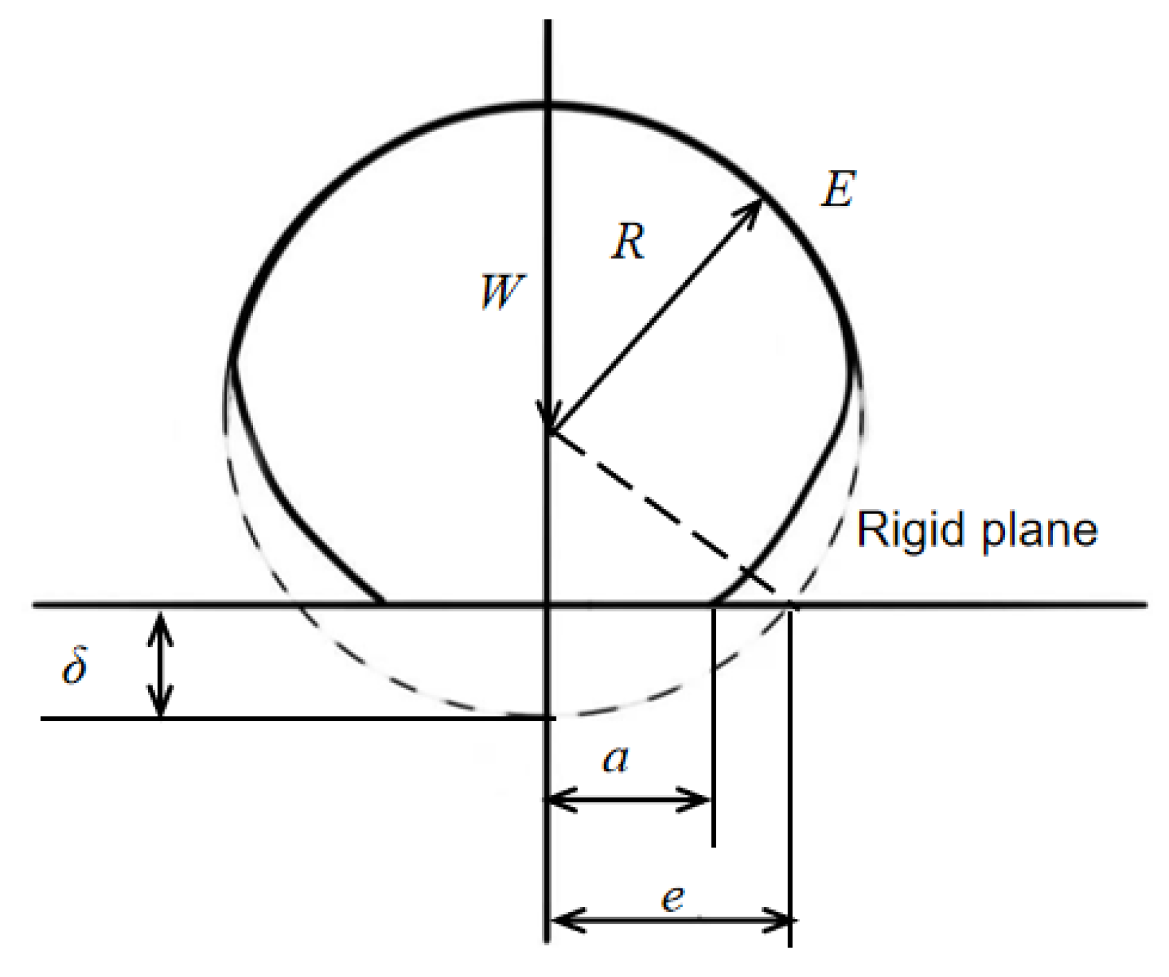
According to the Hertzian contact theory, the actual contact occurs only on a small part of the apparent area due to the surface roughness when two solid surfaces are in contact. The size and distribution of the zone of contact exert a decisive influence on friction and wear. The shape of the rough peaks on the actual contact surface is usually elliptical. Since the size of the contact area of the ellipsoid is much smaller than its radius of curvature, the rough peak can be approximately regarded as a sphere. The contact of two flat surfaces can be regarded as a series of uneven spheres. The contact between two elastomer can be converted into the contact between an elastic sphere with equivalent radius of curvature R and equivalent modulus of elasticity E and a rigid smooth surface.
When μLED contacts with PDMS, the Young’s modulus of PDMS is much lower than that of μLED, so it can be considered as elastic contact. When the two rough peaks contact each other, the normal deformation δ is produced under the action of load W, which makes the shape of the elastic sphere change from dotted line to solid line. The actual contact area is a circle of radius a, as shown in Figure 2. The relationship between load and contact area is given by Equation (2) [22].
δ = ( 9 W 2 16 E * 2 R ) 1 / 3 a = ( 3 W R 4 E * ) 1 / 3 W = 4 3 E * R 1 / 2 δ 3 / 2
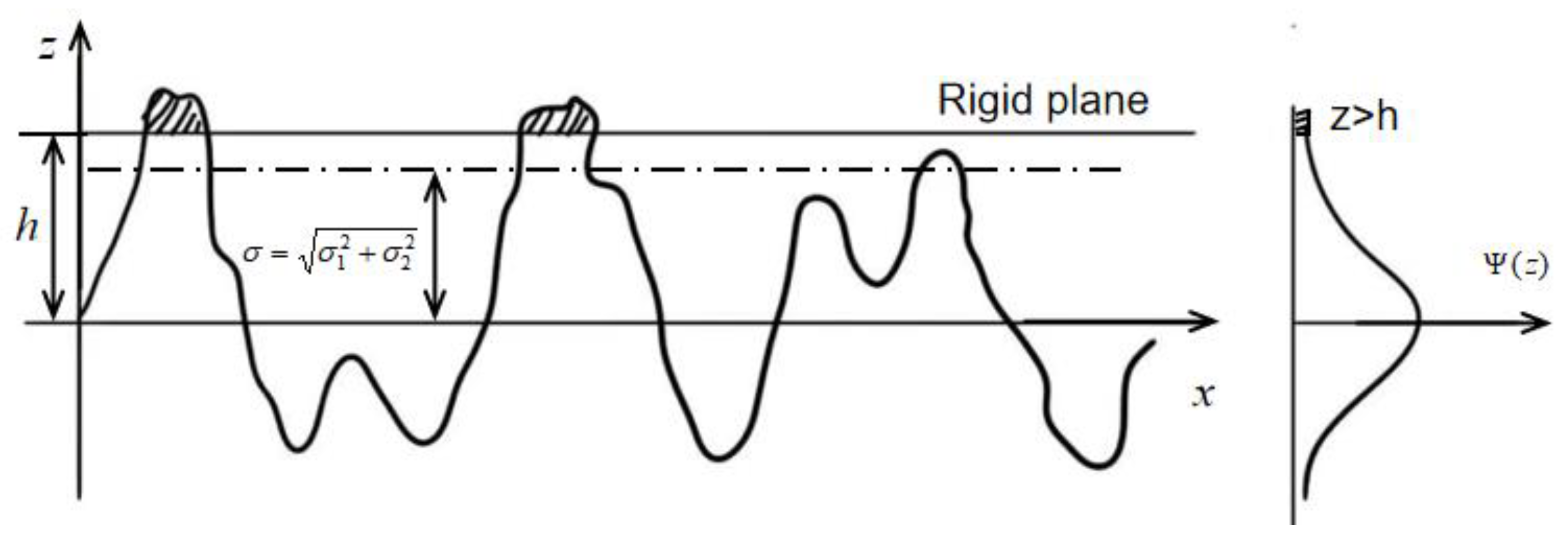
The ideal rough surface is composed of many orderly rough peaks with the same curvature radius and height, and the load and deformation of each peak are exactly the same and independent from each other. However, the rough peak height of the actual contact surface is randomly distributed in general, so the contact peak should be calculated according to the probability. The contact condition of two rough surfaces is shown in Figure 3.
Their contact can be converted into the situation where one smooth rigid surface touches another rough elastic surface. Since the surface of μLED is very smooth, while the surface of PDMS is quite the opposite, this assumption is consistent with reality.
When the distance between the center lines is h, only the part of the contour height z > h contacts with. In the probability density distribution curve, the shading area of the z > h part is the surface contact probability, that is [23]
P ( z > h ) = h ψ ( z ) d z
If the number of peaks on the rough surface is n, the number of peaks participating in the contact, m, is given by [23]:
m = n h ψ ( z ) d z
The normal phase deformation of each contact peak is z-h. From Equation (2), the actual contact area A is given by [23]:
A = m π R ( z h ) = n π R h ( z h ) ψ ( z ) d z
The total load W is supported by the contact peak as [23]:
W = 4 3 m E * R 1 / 2 ( z h ) 3 / 2 = 4 3 n E * R 1 / 2 h ( z h ) 3 / 2 ψ ( z ) d z
Usually, the contour height of the actual surface follows a Gaussian distribution [24], in which most of region near the z-score approximates an exponential distribution. Suppose that ψ ( z ) = exp ( z / σ ) , we get:
m = n σ exp ( h / σ )
A = π n R σ 2 exp ( h / σ )
W = 3 4 n E * R 1 / 2 σ 3 / 2 exp ( h / σ )
From the above equations, it can be derived that W is proportional to A and W is proportional to m. Thus, the actual contact area and the number of contact peaks have a linear relationship with the load in the elastic contact state of the two rough surfaces. Separating μLEDs from PDMSs creates two new interfaces, and the force value Fcr required for this process is obtained as [10]:
F c r = A γ
where γ is the viscosity coefficient of the two surfaces. From Equations (8)–(10), it can be concluded that the adhesive force increases with the increase of preload.

3. The Experimental Results and Discussion

3.1. Experimental Steps

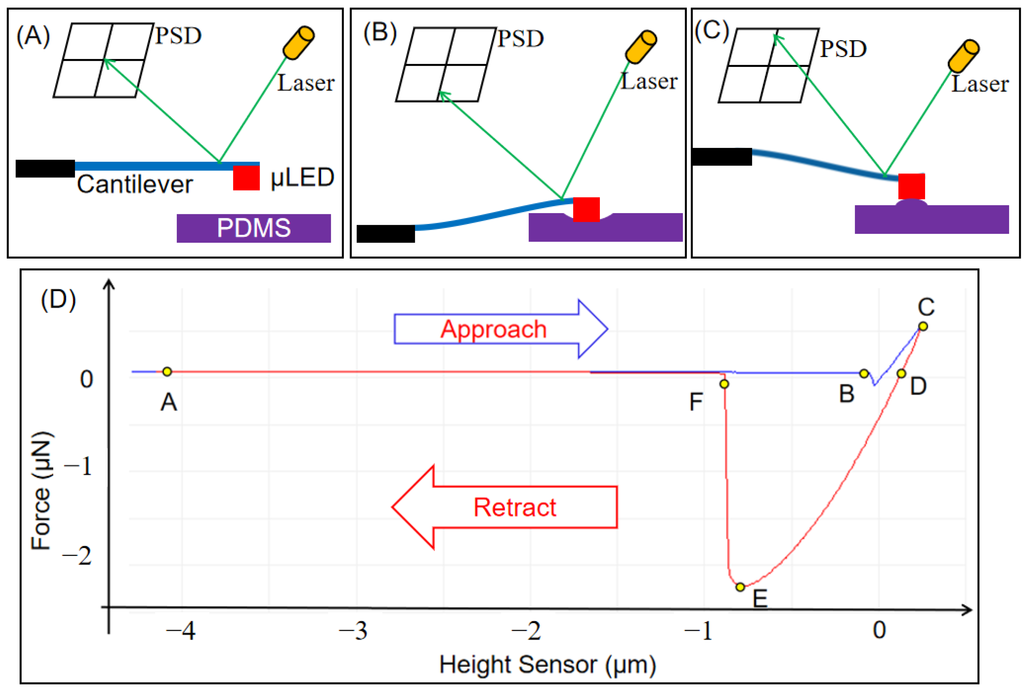
To measure the adhesion between a single μLED and the substrate, a cantilever measurement scheme is adopted, and the specific steps are shown in Figure 4A–C.
Step 1: Apply glue to the tip of the tipless cantilever with a stiffness of 5.1 N/m.
Step 2: Move the cantilever above a μLED.
Step 3: Lower the cantilever to contact the μLED and wait for the glue (UV photoresist) to solidify.
Step 4: Raise the cantilever to make the μLED separate from the base.
Step 5: Move μLED above the PDMS substrate.
Step 6: Measure the relevant force value at different peel speeds and preload.
A typical adhesion–depth curve on a single μLED with a flexible PDMS substrate (1:10 mixing ratio) measured by AFM is shown in Figure 4D. The tip of the cantilever is controlled at a speed of 10 μm/s. The x-axis is the displacement of the μLED. The measurement process is divided into two segments according to the direction of cantilever movement: approach (red line in Figure 4D) and retract (blue line in Figure 4D). The y-axis is force between the μLED and PDMS.
The AFM has been well calibrated using thermal method. The relationship between the force acted on cantilever and PSD output has been obtained before measuring the adhesion force.
The μLED on the cantilever was moved above a substrate PDMS, as shown in Figure 4A. Figure 4B is in a loading status. The μLED is pressed on the PDMS and continuously moved through the precision stage. The laser spot moves as the cantilever bends. The cantilever will not stop until the pressure equals the set preload, as shown in section BC in Figure 4D. Figure 4C is in reverse motion. With the reverse movement, the pressure of μLED on the PDMS substrate becomes smaller and smaller until the pressure reaches 0, as shown in the CD section.
Dynamic jumping behavior during approach (such as the BC segment) and measured jumping behavior during return (CF) were measured.
As can be seen from Figure 4D, the measurement process can be divided into four stages according to the contact status: (I) pressure down to contact with PDMS, (II) pressure to the maximum to reach preload, (III) reverse movement, and (IV) separation from PDMS.
I—Initial state: the cantilever is moved by a precision stage and is not in contact with the PDMS, as shown in Section AB.
II—Loading status: μLED contact PDMS. The μLED is pressed on the PDMS and continuously moved through the precision stage. The laser spot moves as the cantilever bends. The cantilever will not stop until the pressure equals the set preload, as shown in section BC.
III—Reverse motion: With the reverse movement, the pressure of μLED on the PDMS substrate becomes smaller and smaller until the pressure reaches 0, as shown in the CD section. As the reverse motion continues, the PDMS deforms due to the tension between the μLED and PDMS. At this point, the elastic force of the cantilever acting on μLED is less than the critical adhesion force of PDMS, as shown in section DE.
IV—Exit stage: The elastic force of the cantilever on μLED is greater than the critical adhesion force. A sudden jump in the position sensitive device (PSD) voltage output can be observed, as shown in the EF section.
The maximum pull-off force can be defined as the minimum force of the force-depth curve, as shown in Figure 4D.

3.2. Measurement of Adhesion under Different Detaching Velocities and Preload

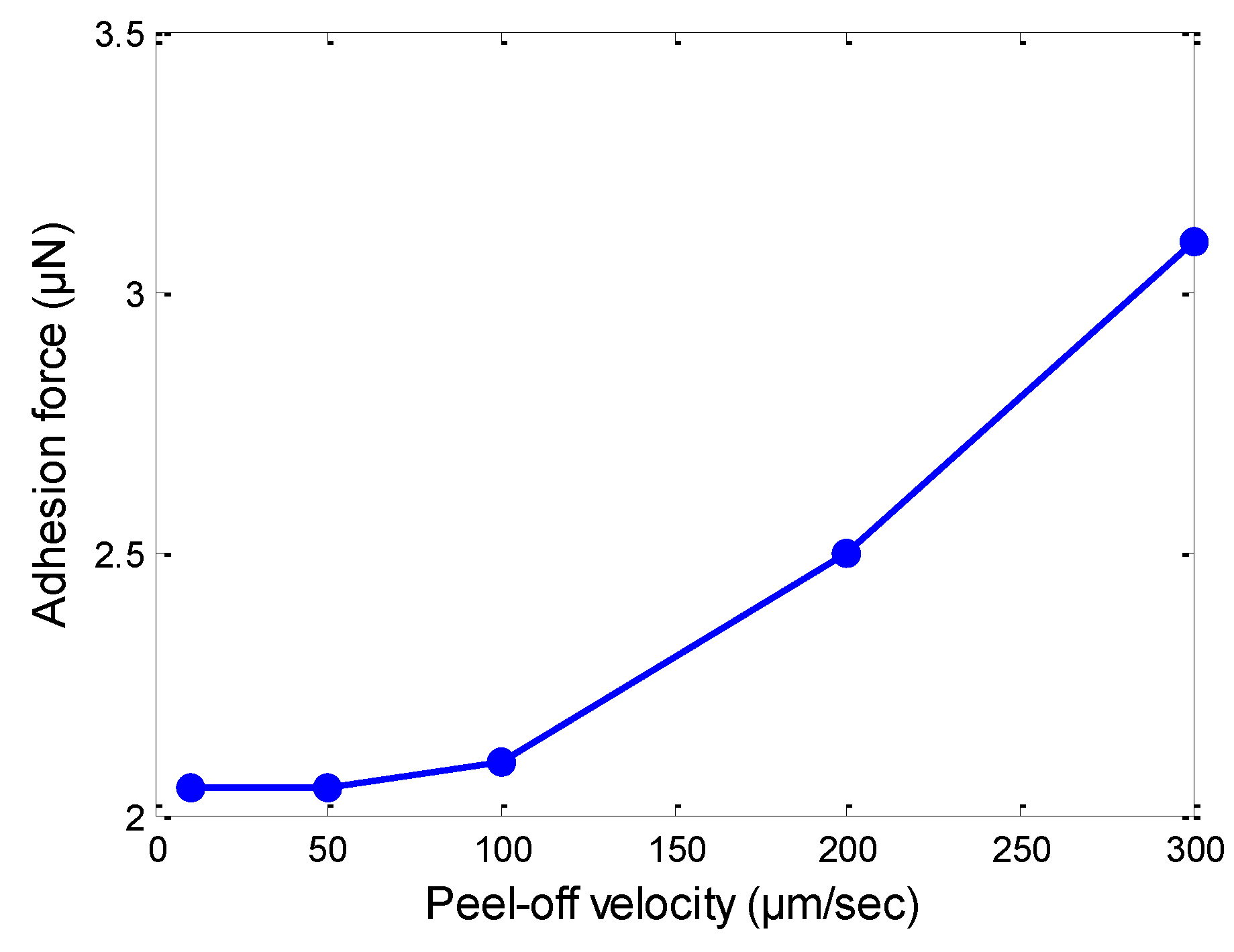
As shown in Figure 5, the maximum pull-off force was measured at different peel velocities (detaching velocity) varying from 10 μm/s to 300 μm/s, in which high peel speed (300 μm/s) resulted in strong adhesion, while low peel speed (10 μm/s) resulted in weak adhesion. Obviously, there is a strong correlation (proportional relationship) between the maximum pull-off force and the peel velocity.
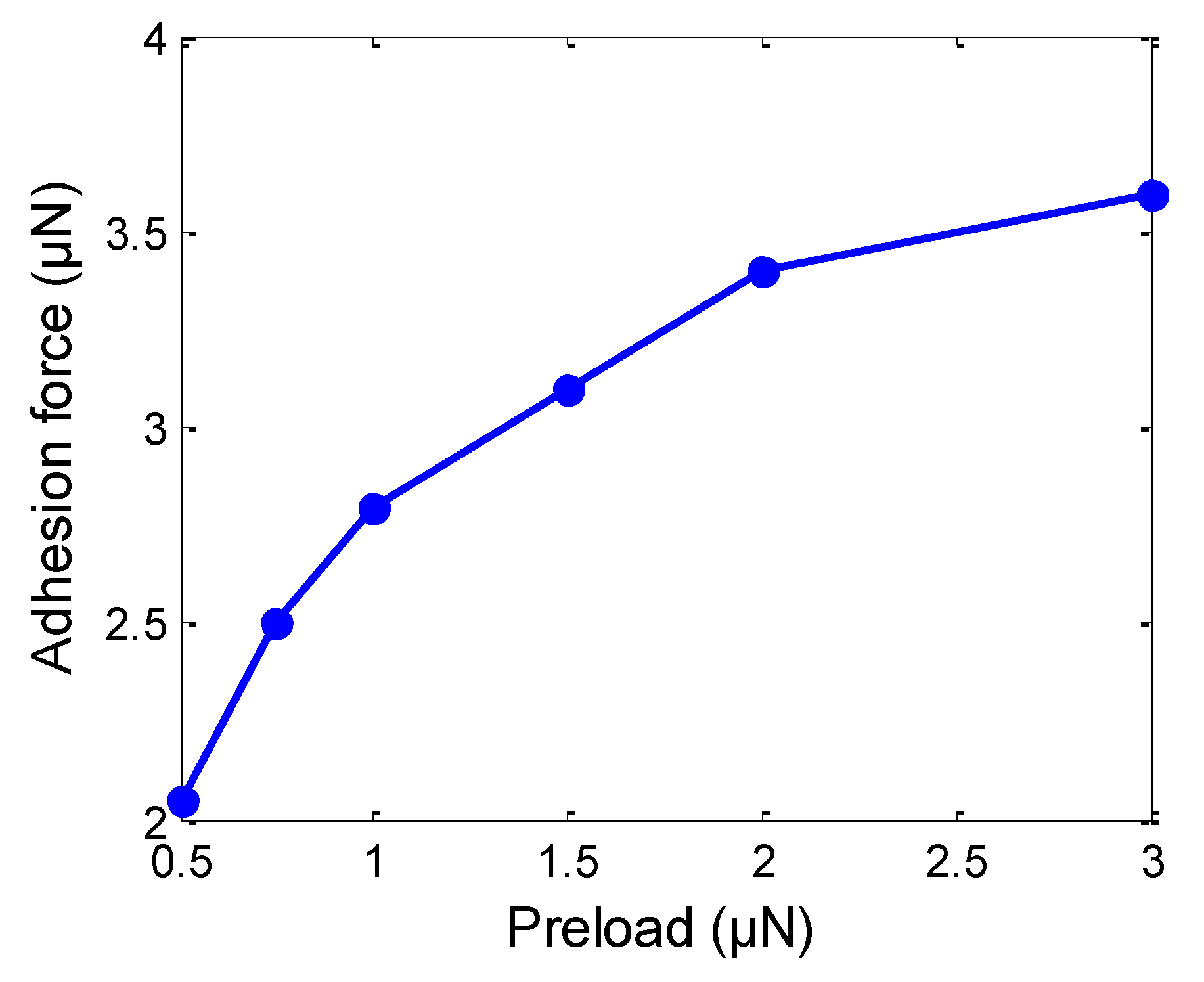
We measured the maximum adhesion force at different preload from 0.5 to 3 μN (the peel speed was fixed at 10 μm/s). The proportional relationship between the maximum pull-off force and the preload is shown in Figure 6.
The experimental results show that the preload has a great influence on the adhesion, which is different from the previous research: “Unlike the effects of material property of PDMS, the maximum pull-off force has similar value regardless of the initial indentation force between the tip and the flexible substrate”. Our theoretical result is consistent with our experimental result but different from the literature.
It Is hard to compare the experimental results to results from Equations (8)–(10). The equations show a positive proportion relationship between contact area and the maximum pull-off force. However, the real contact area between the μLED and PDMS or other substrates could not be measured. Therefore, it is impossible to directly compare the quantity of theoretical value and experimental value absolutely, but only relatively.

4. Conclusions

In this paper, the adhesion force between the μLED and substrate at different peel speeds and preload was measured by AFM. The experimental results show that the separation force between a single μLED and PDMS substrate is not only related to the peel speed, but also related to the preload. Although it is hard to directly compare the absolute quantity of theoretical value and experimental value, the results find a new way to design an apparatus for μLED transfer printing. Future research is required to reversibly change adhesion strength between strong and weak modes by more than two orders of magnitude so that the system can be applied in transfer printing. We will focus on the design of a novel substrate to achieve this target. This system would have broader impacts in transfer printing.

Author Contributions

J.B. and P.N. designed the manuscript, wrote and analyzed the data; J.B. designed the figures for the manuscript and performed the experiments, data collection and/or statistical analysis; P.N., S.C. and Q.L. revised the manuscript. All authors have read and agreed to the published version of the manuscript.

Funding

This research received financial support by the Scientific Research Program of Tianjin Education Commission (No.2019ZD08).

Institutional Review Board Statement

Not applicable.

Informed Consent Statement

Not applicable.

Data Availability Statement

The data that support the findings of this study are available from the corresponding author, P.J.N., upon reasonable request.

Conflicts of Interest

The authors declare that the research was conducted in the absence of any commercial or financial relationships that could be construed as a potential conflict of interest.

References

  1. Virey, E.H.; Baron, N. Status and prospects of microLED displays. SID Symp. Dig. Tech. Pap. 2018, 49, 593–596. [Google Scholar] [CrossRef]
  2. Lianga, C.; Wanga, F.; Huoa, Z.; Shia, B.; Tiana, Y.; Zhaoa, X.; Zhang, D. Pull-off force modeling and experimental study of PDMS stamp considering preload in micro transfer printing. Int. J. Solids Struct. 2020, 193–194, 134–140. [Google Scholar] [CrossRef]
  3. Zhu, G.; Liu, Y.; Ming, R.; Shi, F.; Cheng, M. Mass transfer, detection and repair technologies in micro-LED displays. Sci. China Mater. 2022, 65, 2128–2153. [Google Scholar] [CrossRef]
  4. Kamarei, Z.B. Analysis for science librarians of the 2014 Nobel Prize in physics: Invention of efficient blue-light-emitting diodes. Sci. Technol. Libr. 2015, 34, 19–31. [Google Scholar] [CrossRef]
  5. Park, S.-I.; Xiong, Y.; Kim, R.-H.; Elvikis, P.; Meitl, M.; Kim, D.-H.; Wu, J.; Yoon, J.; Yu, C.-J.; Liu, Z.; et al. Printed assemblies of inorganic light-emitting diodes for deformable and semitransparent displays. Science 2009, 325, 977–981. [Google Scholar] [CrossRef]
  6. Cok, R.S.; Meitl, M.; Rotzoll, R.; Melnik, G.; Fecioru, A.; Trindade, A.J.; Raymond, B.; Bonafede, S.; Gomez, D.; Moore, T.; et al. Inorganic light-emitting diode displays using micro-transfer printing. J. Soc. Inf. Disp. 2017, 25, 589–609. [Google Scholar] [CrossRef]
  7. Kim, T.-I.; Jung, Y.H.; Song, J.; Kim, D.; Li, Y.; Kim, H.-S.; Song, I.-S.; Wierer, J.J.; Pao, H.A.; Huang, Y.; et al. High-efficiency, microscale GaN light-emitting diodes and their thermal properties on unusual substrates. Small 2012, 8, 1643–1649. [Google Scholar] [CrossRef]
  8. Carlson, A.; Bowen, A.M.; Huang, Y.; Nuzzo, R.G.; Rogers, J.A. Transfer printing techniques for materials assembly and micro/nanodevice fabrication. Adv. Mater. 2012, 24, 5284–5318. [Google Scholar] [CrossRef]
  9. Kim, S.; Wu, J.; Carlson, A.; Jin, S.H.; Kovalsky, A.; Glass, P.; Liu, Z.; Ahmed, N.; Elgan, S.L.; Chen, W.; et al. Microstructured elastomeric surfaces with reversible adhesion and examples of their use in deterministic assembly by transfer printing. Proc. Natl. Acad. Sci. USA 2010, 107, 17095–17100. [Google Scholar] [CrossRef]
  10. Tian, Y.; Pesika, N.; Zeng, H.; Rosenberg, K.; Zhao, B.; McGuiggan, P.; Autumn, K.; Israelachvili, J. Adhesion and friction in gecko toe attachment and detachment. Proc. Natl. Acad. Sci. USA 2006, 103, 19320–19325. [Google Scholar] [CrossRef] [Green Version]
  11. Xu, Q.; Wan, Y.; Hu, T.S.; Liu, T.X.; Tao, D.; Niewiarowski, P.H.; Tian, Y.; Liu, Y.; Dai, L.; Yang, Y.; et al. Robust Self-cleaning and Micromanipulation Capabilities of Nano-pads of Gecko Spatulae and their Bio-mimics. Nat. Commun. 2015, 6, 8949. [Google Scholar] [CrossRef]
  12. Yeo, C.; Lee, S.; Polycarpou, A.A. Dynamic adhesive force measurements under vertical and horizontal motions of interacting rough surfaces. Rev. Sci. Instrum. 2008, 79, 015111. [Google Scholar] [CrossRef]
  13. Kim, M.S.; Park, J.; Choi, B. Measurement and analysis of micro-scale adhesion for efficient transfer printing. J. Appl. Phys. 2011, 110, 024911. [Google Scholar] [CrossRef]
  14. Vasilak, L.; Halim, S.M.T.; Gupta, H.D.; Yang, J.; Kamperman, M.; Turak, A. Statistical Paradigm for Organic Optoelectronic Devices: Normal Force Testing for Adhesion of Organic Photovoltaics and Organic Light-Emitting Diodes. ACS Appl. Mater. Interfaces 2017, 9, 13347–13356. [Google Scholar] [CrossRef]
  15. Yeo, C.; Lee, J.; Polycarpou, A.A. Dynamic adhesive forces in rough contacting bodies including normal and sliding conditions. J. Adhes. Sci. Technol. 2012, 26, 2709–2718. [Google Scholar] [CrossRef]
  16. Lee, J.; Maharjan, J.; He, M.; Yeo, C. Effects of system dynamics and applied force on adhesion measurement in colloidal probe technique. Int. J. Adhes. Adhes. 2015, 60, 109–116. [Google Scholar] [CrossRef]
  17. Zheng, Y.; Song, L.; Hu, G.; Zhao, M.; Tian, Y.; Zhang, Z.; Fang, F. Improving environmental noise suppression for micronewton force sensing based on electrostatic by injecting air damping. Rev. Sci. Instrum. 2014, 85, 055002. [Google Scholar] [CrossRef]
  18. Lee, M.H.; Lim, N.; Ruebusch, D.J.; Jamshidi, A.; Kapadia, R.; Lee, R.; Seok, T.J.; Takei, K.; Cho, K.Y.; Fan, Z.; et al. Roll-to-roll anodization and etching of aluminum foils for high-throughput surface nanotexturing. Nano Lett. 2011, 11, 3425–3430. [Google Scholar] [CrossRef]
  19. Liang, C.; Wang, F.; Huo, Z.; Shi, B.; Tiana, Y.; Zhang, D. Adhesion performance study of a novel microstructured stamp for micro-transfer printing. Soft Matter. 2021, 17, 4989. [Google Scholar] [CrossRef]
  20. Qiu, P.; Zhu, S.; Jin, Z.; Zhou, X.; Cui, X.; Tian, P. Beyond 25 Gbps optical wireless communication using wavelength division multiplexed LEDs and micro LEDs. Opt. Lett. 2022, 47, 317–320. [Google Scholar] [CrossRef]
  21. Feng, X.; Meitl, M.A.; Bowen, A.M.; Huang, Y.; Nuzzo, R.G.; Rogers, J.A. Competing fracture in kinetically controlled transfer printing. Langmuir 2007, 23, 12555–12560. [Google Scholar] [CrossRef] [PubMed]
  22. Shizhu, W. Principles of Tribology, 2nd ed.; Tsinghua University Press: Beijing, China, 2017. [Google Scholar]
  23. Bowden, F.P.; Tabor, D. The Friction and Lubrication of Solid; Clarenden Press: Oxford, UK, 1964. [Google Scholar]
  24. Johnson, K.L. Contact Mechanics; Cambridge University Press: London, UK, 1985. [Google Scholar]
Figure 1. Image of μLED. (A) Scanning electron microscope (SEM) image of μLED. (B) The surface of the μLED array obtained by optical microscope.
Applsci 12 09480 g001
Figure 2. Diagram of single peak elastic contact.
Applsci 12 09480 g002
Figure 3. Contact of rough surfaces. The root mean square values of the roughness of the two surfaces are respectively σ1 and σ2, h is the distance between the center lines, z is the part of the contour height z > h contacts with, and Ψ(z) is the probability of the surface contact.
Applsci 12 09480 g003
Figure 4. The adhesion measurement results based on cantilever between μLED and substrate. (AC) Measurement steps. (A) The initial state. (B) The loading status. (C) The reverse motion. (D) Typical single measurement results.
Applsci 12 09480 g004
Figure 5. The measured maximum pull-off forces with respect to peel velocity.
Applsci 12 09480 g005
Figure 6. Results for the maximum pull-off force at different preload.
Applsci 12 09480 g006
Publisher’s Note: MDPI stays neutral with regard to jurisdictional claims in published maps and institutional affiliations.