Abstract
In this article we present a theoretical investigation of gold-silica-silver nanostructures and their optical properties with respect to ultrafast electronic applications and coherent control by tailored optical fields. We found a remarkable sensitive behavior to the carrier envelope phase (CEP) of the driving laser pulses in the coupling of surface and bulk plasmons leading to a superposition of distinct modes with a time-dependent amplitude structure. Furthermore, we show a rather complex temporal evolution of plasmonic surface modes. Our results suggest the potential for coherent control of the time-dependent resonant coupling between surface and volume modes by tailored laser pulses and foster the field of time-dependent spectroscopy of thinfilm hybrid nanostructures with single layer thickness down to the two-dimensional limit.
1. Introduction
The development of plasmonic assistend sensors is a hot topic in research and provides broad range of applications driven by biomedical sensing and lab-on-a-chip applications [1,2,3]. Tailored geometries demonstrate complex dynamic behavior for improved sensing and electrooptical coupling. Especially their properties under broken symmetry [4] and the formation of whispering gallery modes [5] determine new routes in the developemnt of tailored plasmonic structures and their time dynamic behavior.
The availability of ultrafast time-resolved spectroscopy methods of light and electrons enabled the investigation of dynamics on timescales down to attosecond duration [6,7,8] not only in the gas phase, but also in solid samples. However, the combination of ultrafast time resolution and nanometer spatial resolution is experimentally challenging and facing a nearly unexplored field in experimental ultrafast science. In 2007 Stockman et al. proposed the attosecond nanoplasmonic field microscope [9]. Lupetti et al. demonstrated the technique of attosecond photoscopy [10]. Both concepts theoretically demonstrate that ultrafast science at ultrasmall structures with high temporal and spatial resolution down to attosecond duration and nanometer spatial resolution is feasible and experimentally accessible. Imaging electric fields on the nanoscale has been demonstrated by several groups [11,12,13,14] and even the dynamic behaviour has been retrieved by Kubo et al. [15] and Mårsell et al. [16,17] imaging the plasmonic fields of a propagating plasmon on a silver grating and in silver nanowires, respectively, by interferometric time-resolved photoelectron emission micrographs (ITR-PEEM).
Resolving the time dependent behaviour of plasmonic systems has been limited to the spectral domain for a long period of time. The availability of ultrafast laser pulses in the femto- and even attosecond range provides access to the realtime measurements of these dynamics following new excitation schemes [18]. Even more complex nanostructures as coupled particles, resonators, or coupled antenna structures exhibiting complex dynamic temporal as well as spatial modulations of the electric field on subcycle time scale [15,16,19] are in the focus of current research.
Prodan et al. [20] describe in the model of plasmon hybridization the spatial characteristics of complex nanostructures under resonant excitation. Plasmonic coupling in hybrid nanoscopic systems builds up a symmetrical (bright) mode, where the charge density is unilateral modulated as a dipole or an antisymmetrical (dark) mode forming a multipole. Gómez et al. [21] demonstrated that the excitation of antisymmetrical modes is only possible from the interaction of bright modes, inhomogeneous far-field illumination or related excitation schemes.
The observations presented in this article are related to nearfield phenomena of strongly coupled plasmons which has been discussed by Schertz et al. [22]. Besides the strong coupling hybridization is of major importance to explain the formation of whispering gallery modes after excitation and an enhanced lifetime of the plasmon itself. The hybrid structure presented in this paper is comparable to the geometry and study presented by Chang et al. [23] analysing a symmetric tripple layer nano sandwich structure with respect to the excitation and superposition of dark and bright plasmonic modes.
With respect to early studies on this topic [24] our studies presented here are focused on ultrafast mode coupling and coherent control on a gold-silica-silver nanodisk system. Nevertheless, we compare our studies again to Dmitriev et al. studying the hybridization in Au-SiO-Au nanodisk sandwiches [25] in bulk media and compared extinction measurements to simulations. The sandwiches are composed of two gold disks (radius 55 nm and 44 nm, height 10 nm) that are separated by an insulating silica disk (diameter adapting top and bottom disk, height 10 nm). Hybridization in this system originates from two possibilities of dipole arrangements in the top and bottom gold disks. In the high energy state the dipole moments are aligned parallel, whereas in the low energy state anti-parallel. In [24] it is demonstrated, that hybridization is sensitive to the top layer thickness of a gold-silica-gold sandwich as well as the different diameters of the top and bottom disks.
The temporal characteristics and in particular build-up time of the plasmonic fields in such hybridized resonators goes down to a few femtoseconds. According to the experimental techniques available in ultrafast time resolved spectroscopy today [8], the direct observation of ultafast plasmon dynamics in such systems with a temporal resolution down to a few ten attoseconds, by attosecond streaking, can be adapted [10].
Studies based on nanodisk resonator structures with the thickness of the larger top disk decreased down to a few monolayers (1 nm formed by 2.5 monolayers) are presented. The plasmonic excitation in this type of nanoresonator is refined to the surface without any volume excitation observable at the surface layer. The key parameters for this behavior are analyzed and discussed. In contrast to our studies in [24] we are discussing a gold-silica-silver sandwich excited by laser pulses with different CE-phase resulting in a dedicated excitation of surface modes. Furthermore, we observe the formation of whispering gallery modes on the thin top layer after excitation.
In particular the asymmetry of the diameter between top and bottom disk is identified as a key parameter for the predominant excitation of surface modes. The changes of absorption cross sections, electric near fields, and the temporal evolution of the electric near fields on a sub-femtosecond timescale are represented with respect to the exciting laser pulse and at different radii of the nano sandwich resonators.
2. Methods
The simulations presented in this article were performed using the finite integration technique (FIT) [26] within the Computer Simulation Technology (CST) Studio Suite. This approach is similar to the finite difference time domain (FDTD) technique used for example in MEEP [27] or Lumerical [28]. With this approach the Maxwell’s equations in the time domain either in integral form (FIT) or differential form (FDTD) are solved to study the temporal evolution of the local distribution of electromagnetic fields. The target geometry is divided into small subvolumes with optimized shape and the electric and magnetic field is numerically retrieved for each time step. The simulation setup is identical to the one used in [24] and verified against the simulations and results presented in [25].
In [24] the sandwich geometry of a gold-silica-gold sandwich structure was optimized in the corresponding layer thicknesses and diameter ratios to provide a time dependent superposition of a maximum number of modes, excited by an ultrafast fourier limited laser pulse. In the simulation presented here, the final geometry is adapted without any further optimization focussing on the dynamics of the driving laser field and the appearance of whispering gallery modes due to geometrical symmetry breaking.
The sandwich is composed of three individual disks with a gold bottom disk, a silica center disk and a silver top disk as depicted in Figure 1. The initial diameters of the bottom and top disks are 88 nm and 108 nm, respectively. The center disk shape is conical and adapts to the disks below and above. The disk thickness of the bottom and center disks are 10 nm and of the top disk 1 nm. We excite the plasmonic oscillation with an ultrafast laser pulse with a Fourier limited pulse duration of below fs covering a spectral range from 550 to 1500 nm in normal incidence (see Figure 2). The carrier envelope phase (CEP) of the electric field is corresponding to a sine-like electric field.
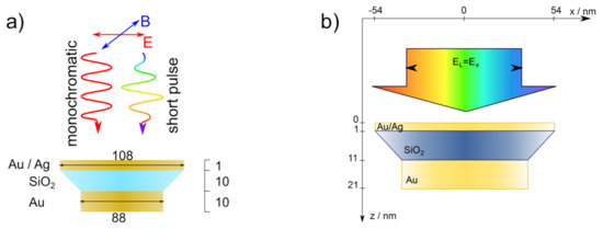
Figure 1.
A gold-silica-silver nanodisk sandwich is illuminated from above with an linearly polarized ultra short laser pulse ( nm, fs) or monochromatically at the resonance wavelength. The sandwich has a total height of 21 nm and a radius of 54 nm of the top thin disk and 44 nm of the bottom thick disk. The geometry is unchanged in all simulations. Only the driving fields are varied in terms of the CE-phase. (a) Simulation geometry, adapted with permission from [24] ©The Optical Society; (b) Simulation setup.
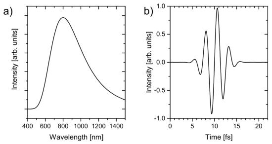
Figure 2.
Excitation pulses used in the nanodisk sandwich simulations. (a) The spectrum; (b) the normalized temporal electric field. Reprinted with permission from [24] ©The Optical Society.
Different observation monitors were used to investigate the behavior of the sandwiches in energy and time domain:
- Absorption cross section;
- Electric field;
- Temporal evolution of electric field.
In the simulation presented in this paper, the dielectric function for gold is taken from [29]. We want to emphasize that the dielectric properties change [30] for ultrathin films. Especially with respect to physical properties like the formation of islands and the coalescence during the growth process approaching the quantum limit of atomically thin films in particular is not included in our model. Nevertheless, Wang et al. [31] demonstrated experimentally that gold film thicknesses from two to ten nanometers could be carefully treated in the Drude circle regime. They identified the cluster size in film growth as the predominant cause for permitivity changes. Campbell et al. [32] support this finding theoretically comparing the permitivity changes to the Lorentz–Drude model for the visible wavelength range. The plasmon in the simulations presented here is excited with an electric field direction in the surface plane corresponding to the direction of extended material where the influence of the film thickness to the permitivity is smaller compared to the out-of-plane component [33].
As a consequence, the presented results rely on the data for the dielectric function that are restricted to a Lorentz–Drude model. As a systematic simulation within a Lorentz–Drude model we trust our results within the range of the film thickness presented according to a careful evaluation of the optical properties in the given thickness range.
2.1. Simulation Setup
The aim of this study is the investigation of the influence of the confinement of bulk plasmons in thin layer thickness in a triple layer nanodisk structures. A bulk plasmon needs a certain volume for its electronic oscillations. If the volume is now confined in one dimension by reducing the thickness, the electronic oscillations are perturbed and the response changes. The nanodisk structures are composed of a gold bulk layer covered by an insulating silica layer and a thin silver top layer as already presented in Figure 1. The plasmon is excited either by a ultrafast laser pulse ( nm, fs, see Figure 2) or monochromatically at the resonance wavelength, which will be discussed later.
In the (10-10-1) gold-silica-silver sandwich simulation the bottom disk has a thickness of 10 nm and a diameter of 88 nm, the top silver disk has a thickness of 1 nm and a diameter of 108 nm. The silver unit cell size has almost the same value as gold and is [34]. Therefore, the top silver disk is formed by 2.5 monolayers. The silica spacer has a conical shape and a thickness of 10 nm.
For the simulation of absorption spectra and electric near fields of the disk sandwich the sample is illuminated from above perpendicular to its surface by linearly polarized light as already defined in Figure 1.
The nanodisk sandwich is excited with Fourier limited light pulses with a spectral range of 550 nm to 1500 nm. The spectrum and the temporal electric field are shown in Figure 2a,b, respectively. The electric field of the laser pulses exhibit a carrier envelope phase of , corresponding to a sine-like pulse.
In all simulations, the bottom and spacing disks are meshed with a 1 nm grid in all three spatial directions. The thin disk is meshed in the surface plane with the same 1 nm grid, but perpendicular to the surface with a nm grid. The boundary conditions are defined to be “open”, which means adding space around the structure, where the electric field of the light pulse and the structure itself are vanishing. By this definition of the simulation environment, the electric field of the pulse is absorbed at the edges of the simulation box, which is even bigger than the simulated structure. Since we observed complex electric field shapes forming whispering gallery modes [35], we did not use any symmetry approaches in simulation to reduce computation time. The CST simulation setup allows for different grid sizes per layer. The volumetric grids are chosen to be 1 nm for the bottom gold and center silica disk of 10 nm thickness and 0.1 nm for the silver top disk.
2.2. Plasmonic field Evolution in a Thin Gold Nano Disk after Ultrafast Excitation
The absorption resonance of a disk is mainly determined by its diameter [36]. A variation results in a resonance shift either to shorter wavelength (decreasing diameter) or longer wavelength (increasing diameter). In the case of very thin disks the absorption is also shifted with increasing disk diameter to shorter wavelength. The resonance shift follows an exponential behaviour corresponding to the aspect ratio of thickness and diameter.
The electric field presented in Figure 3a at the surface of a gold disk is induced by plasmonic excitation with monochromatic light at the resonance wavelength.
Figure 3.
(a) Electric near field at the surface of a 1 nm thick gold disk excited with monochromatic light at 1390 nm and (b) the temporal evolution of the integrated field over the left and right half disk after excitation with a broadband pulse together with the excitation signal.
The near field shows a dipole structure with the polarization axis as the symmetry axis. One half of the disk is negatively charged, the other positively with a smooth transition. The temporal evolution of the integrated field of the two half disks together with the excitation signal is shown in Figure 3b. The driving light field induces a dipolar field that oscillates slightly slower than the driving field. In one plasmonic field cycle the laser electric field builds up, then decreases and reverses to opposite polarity. After one cycle the field returns to the initial polarisation. During the plasmon build up time, the electric field strength grows. The duration of the plasmon build up is almost as long as the driving laser pulse: the maximum of the excitation signal is reached around 10 fs, whereas the plasmonic field still builds up, and reaches its maximum at around 13 fs. The laser field has almost vanished at the maximum of the plasmonic field. After the plasmon build up, the electric field oscillates on the disk and is damped over time.
The plasmon dephasing takes 32 fs until the plasmonic field has decreased its field strength to . For the plasmonic response of a single disk follows, that the resonance shifts with decreasing diameter and increasing thickness to shorter wavelength, and the plasmonic field on the disk surface is represented by one dipole. Once excited, the field builds up and is then damped within several ten femtoseconds. As we will see, in the case of the gold-silica-silver nano sandwich system, this behaviour is strongly changed by coupling effects, resulting in the time-dependent evolution of plasmonic surface modes as well as whispering gallery modes.
3. Ultrafast Plasmon Modes in Gold-Silica-Silver Sandwiches
In the following section we present the simulation of time dependent field dynamics in a gold-silica-silver sandwich (Figure 1 driven by a ultrafast laser pulse, with the spectral and temporal properties presented in Figure 2).
From our simulation we retrieve the absorption cross-section of the system shown in Figure 4a.
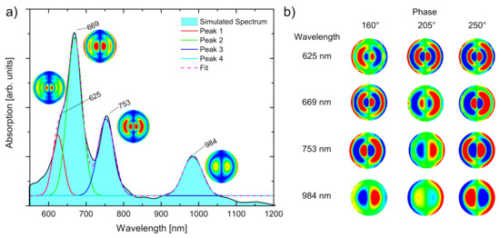
Figure 4.
Excitation of surface modes in a gold-silica-silver sandwich. (a) The absorption spectrum with the time averaged electric near field of monochromatic excitation; (b) shows the evolution of the electric near field at different phase values.
The absorption shows several resonance peaks that can be attributed to different electric field modes, similar to the modes in the gold-silica-gold sandwich we discussed in [24]. The corresponding time averaged electric field of the modes are shown next to the absorption peaks, which can be identified as fundamental TEM 11-TEM 41 modes.
According to further simulations, a variation of the phase of the driving electric field results in a significant change of the excited field distribution within the first half-cycle of the driving field presented in Figure 4b. The phase was chosen for the strongest variation in the field pattern for each of the resonances. At 625 nm one oberserves a minimum/maximum (min/max) pair with opposite polarity at 160 with respect to the center. Another phase shift of 45 shows four alternating min/max pairs. This pattern does not change significantly within another phase shift of 45.
The second resonance at 669 nm starts with four min/max pairs at a phase of 160. A phase shift of 45 leads to a reduction to only two clear modes in the center of the disk. At the rim of the disk alternating min/max spots become visible driving the build up of a ring mode in the oscillator. Another phase shift of 45 leads to a vanishing of the ring mode with three remaining min/max pairs with opposite polarity of the center pair.
The third resonance at 753 nm is composed of three alternating min/max pairs, which inverts within a phase shift of 90 instead of 180. In the intermediate state only two min/max pairs with the same polarity appear. The outer min/max pair at the rim of the disk shows again a circular modulation but without polarity changes.
The fourth resonance at 984 nm features only two min/max pairs that change their polarity within 90.
Comparing the different structures one can see the phase dependent excitation of different TEM modes at different resonant wavelength, which already demonstrates the feasibility of time dependent coherent control by tailored light fields.
To more closely examine the excitation of whispering gallery modes, we analyse the time dependent field dynamics at two different radii of the top silver disk. Figure 5a,b show the evolution of the plasmonic field along a concentric half circle for radii of 22 nm and 48 nm, respectively.
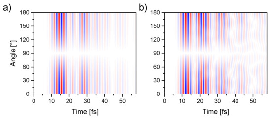
Figure 5.
Evaluation of the electric field on the sandwich surface along a ring with radius (a) 22 nm and (b) 48 nm showing the volume mode in the inside and the ring modes in the outside appearing after around 35 fs.
For the inner radius of 22 nm in (a) only a regular dipole mode is visible arising with the excitation and changing its polarity consecutively with a sinusoidal superposition resulting in additional intensity modulation of the electric field. The dipole oscillation is decaying exponentially within 60 fs to . At 90 the polarization vector of the driving field is perpendicular to the symmetry axis. In the outer ring close to the edge of the disk suddenly after excitation a dipole mode dominates the behaviour up to 40 fs. In the evolution of the field an asymmetric circular ring mode emerges. The circular mode can be figured out by the changing polarity along the line at a constant time step close to 40 fs and 50 fs. Up to eight poles are emerging, driving a ring current at the outer rim of the structure. These ring modes are usually excited with the resonant coupling of a propagating plasmon from a wave guide to a ring resonator. In the case demonstrated in this paper, a slight asymmetry of the electric field of the excitation pulse induces the build up of an asymmetric charge distribution. This asymmetry in time can be seen in (a, b) close to 35 fs.
Figure 6a represents the time dependent behaviour of the electric field at the top disk surface along the axis. In (b) the electric field evolution at two specific positions ( 10 nm and 22 nm) and the related field asymmetry is characterized.
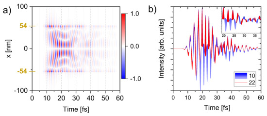
Figure 6.
Electric field along a line on the surface (a) and the field on two positions at 10 and 22 nm (b). The observed line is parallel to the incident field.
In (a) the gradient along the field free lines in between the modes determines the propagation direction. A positive gradient represents a propagation from the center to the rim whether a negative gradient represents a propagation from the rim to the center of the disk. Up to 25 fs we see a propagation of the modes towards the center of the disk followed by a phase jump. Afterwards, the propagation direction changes and the modes are propagating from the center to the rim until 30 fs, where the direction changes again. This switching repeats for several times. The temporal evolution along the line shows an outer mode splitting that happens constantly over the whole time window. A mode splitting of the inner volume mode into two surface modes is observed at around 18 fs and lasts for about 8 fs until the modes are uniting again.
The modes split up more irregularly after that position. Around 28 fs the inner mode splits again but at a lateral position closer to the rim of the disk and the two modes are only slightly shifted with respect to each other. The outer one is merging around 37 fs with the outermost mode. After the phase jump at 30 fs another splitting of the inner mode with only a slight shift is observed. Both modes exist over the whole time window but the splitting position oscillates laterally between 19 nm and 27 nm.
The time dependent intensity envelope, integrating the simulated electrical nearfield of the top disc in the form
provides information on the buildup time to be in the order of and the lifetime of , respectively.
In (b) the electric field intensity at the position of the volume mode at 10 nm (blue line) and the splitting into the surface mode at 22 nm (red line) are shown. The top blue and bottom red shaded areas correspond to the regions where the field at 22 nm is stronger than the field at 10 nm and the other way around. The asymmetry of the area corresponds to different mode velocities. Before 15 fs the intensity of the volume mode is stronger in the outer part. Then the intensity of the inner volume mode increases over time and dominates. At later times the intensity ratio switches again several times indicated by the colour switching of the shaded areas in the graph. In the inset of Figure 6b and the behavior between 30 fs and 40 fs it is shown, that phase jumps and asymmetries in locally distributed field strength happen at attosecond or at least subcycle time-scales in the gold-silica-silver nano sandwich.
4. Conclusions
In this paper we presented simulations on hybrid gold-silica-silver nano sandwich resonators demonstrating a circular asymmetry in their time dependent evolution of the excited plasmonic fields. The build up of ring modes (whispering gallery mode) are observed leading to the formation of a corresponding ring current. To our current understanding, this behavior originates from the asymmetries of the driving electric field of the excitation pulse.
The broken geometrical symmetry and the strong plasmon coupling by the ultrathin layers support the time-dependent behavior and the formation of higher order as well as whispering gallery modes. A comparison to Chang et al. [23] for symmetrical hybrid nanodiscs provide identical timescales for the plasmonic lifetimes. Even though, the rise of high order modes can be attributed to the broken strong coupling geometry. Especially the volume, surface and whispering gallery mode formation should be investigated in more detail according to the experimental availability of tailored electric fields from field synthesis of ultrashort driving pulses in the few-cycle regime [37,38].
In contrast to our prior work [24] in this topic, the special characteristics of the gold-silica-silver sandwich demonstrate a significant phase dependency of the driving electric field which suggests further investigation into tailored pulses and especially CEP dependence.
A current drawback from an experimental perspective is the manufacturability of these structures with standard methods like PVD, MSD, FIB and comparable methods. The top layer having a thickness of only a few monolayers needs ideal roughness and closed and defect free layers at the same time. This requires alternative approaches or material developments to achieve homogenity in terms of a closed and smooth surface, which are currently not solved. Further investigations are clearly assigned to manufacturing capabilities of these structures. A promising route is the replacement of the top layer by double or triple layer 2D materials as well as new systems like intercalated gold and silver into graphene [39]. Using this approach opens up a route to transfer the basic idea provided in this article also to an experimental realization.
Author Contributions
Idea and Concept, J.H.; Data curation, J.E.; Formal analysis, J.H., J.E. and K.L.; supporting simulations, J.E. and K.L.; Supervision, T.U.; Writing—original draft, J.H. and T.U.; Writing—review & editing, J.H. and T.U. All authors have read and agreed to the published version of the manuscript.
Funding
We acknowledge support by the Landesexzellenzcluster “Frontiers in Quantum Photon Science” Hamburg and the Joachim Herz Stiftung.
Data Availability Statement
The data presented in this study are available on request from the corresponding author.
Acknowledgments
We are grateful to Walter Pfeiffer and Mattia Lupetti for fruitful discussions.
Conflicts of Interest
The authors declare no conflict of interest. The funders had no role in the design of the study; in the collection, analyses, or interpretation of data; in the writing of the manuscript, or in the decision to publish the results.
References
- S.S. dos Santos, P.; M. M. M. de Almeida, J.; Pastoriza-Santos, I.; C. C. Coelho, L. Advances in Plasmonic Sensing at the NIR—A Review. Sensors 2021, 21, 2111. [Google Scholar] [CrossRef]
- Li, M.; Cushing, S.K.; Wu, N. Plasmon-enhanced optical sensors: A review. Analyst 2015, 140, 386–406. [Google Scholar] [CrossRef] [PubMed] [Green Version]
- Adhikari, R.; Chauhan, D.; Mola, G.T.; Dwivedi, R.P. A review of the current state-of-the-art in Fano resonance-based plasmonic metal-insulator-metal waveguides for sensing applications. Opto-Electron. Rev. 2021, 29, 148–166. [Google Scholar] [CrossRef]
- Misbah, I.; Zhao, F.; Shih, W.C. Symmetry Breaking-Induced Plasmonic Mode Splitting in Coupled Gold–Silver Alloy Nanodisk Array for Ultrasensitive RGB Colorimetric Biosensing. ACS Appl. Mater. Interfaces 2019, 11, 2273–2281. [Google Scholar] [CrossRef] [PubMed]
- Wang, Y.; Zeng, S.; Humbert, G.; Ho, H. Microfluidic Whispering Gallery Mode Optical Sensors for Biological Applications. Laser Photonics Rev. 2020, 14, 2000135. [Google Scholar] [CrossRef]
- Itatani, J.; Quéré, F.; Yudin, G.L.; Ivanov, M.Y.; Krausz, F.; Corkum, P.B. Attosecond Streak Camera. Phys. Rev. Lett. 2002, 88, 173903. [Google Scholar] [CrossRef] [Green Version]
- Goulielmakis, E. Direct Measurement of Light Waves. Science 2004, 305, 1267–1269. [Google Scholar] [CrossRef] [Green Version]
- Cavalieri, A.L.; Müller, N.; Uphues, T.; Yakovlev, V.S.; Baltuška, A.; Horvath, B.; Schmidt, B.; Blümel, L.; Holzwarth, R.; Hendel, S.; et al. Attosecond spectroscopy in condensed matter. Nature 2007, 449, 1029–1032. [Google Scholar] [CrossRef]
- Stockman, M.I.; Kling, M.F.; Kleineberg, U.; Krausz, F. Attosecond nanoplasmonic-field microscope. Nat. Photonics 2007, 1, 539–544. [Google Scholar] [CrossRef]
- Lupetti, M.; Hengster, J.; Uphues, T.; Scrinzi, A. Attosecond Photoscopy of Plasmonic Excitations. Phys. Rev. Lett. 2014, 113, 113903. [Google Scholar] [CrossRef] [Green Version]
- Kociak, M.; Stéphan, O. Mapping plasmons at the nanometer scale in an electron microscope. Chem. Soc. Rev. 2014, 43, 3865. [Google Scholar] [CrossRef]
- Myroshnychenko, V.; Nelayah, J.; Adamo, G.; Geuquet, N.; Rodríguez-Fernández, J.; Pastoriza-Santos, I.; MacDonald, K.F.; Henrard, L.; Liz-Marzán, L.M.; Zheludev, N.I.; et al. Plasmon Spectroscopy and Imaging of Individual Gold Nanodecahedra: A Combined Optical Microscopy, Cathodoluminescence, and Electron Energy-Loss Spectroscopy Study. Nano Lett. 2012, 12, 4172–4180. [Google Scholar] [CrossRef] [Green Version]
- Douillard, L.; Charra, F. High-resolution mapping of plasmonic modes: Photoemission and scanning tunnelling luminescence microscopies. J. Phys. D Appl. Phys. 2011, 44, 464002. [Google Scholar] [CrossRef]
- Losquin, A.; Lummen, T.T.A. Electron microscopy methods for space-, energy-, and time-resolved plasmonics. Front. Phys. 2017, 12, 127301. [Google Scholar] [CrossRef]
- Kubo, A.; Onda, K.; Petek, H.; Sun, Z.; Jung, Y.S.; Kim, H.K. Femtosecond Imaging of Surface Plasmon Dynamics in a Nanostructured Silver Film. Nano Lett. 2005, 5, 1123–1127. [Google Scholar] [CrossRef]
- Mårsell, E.; Losquin, A.; Guo, C.; Harth, A.; Lorek, E.; Miranda, M.; Arnold, C.; Xu, H.; Mauritsson, J.; L’Huillier, A.; et al. Spatiotemporal imaging of few-cycle nanoplasmonic fields using photoemission electron microscopy. In European Microscopy Congress 2016: Proceedings; Wiley-VCH Verlag GmbH & Co. KGaA: Weinheim, Germany, 2016; Volume 1123, pp. 1144–1145. [Google Scholar] [CrossRef] [Green Version]
- Chew, S.H.; Pearce, K.; Späth, C.; Guggenmos, A.; Schmidt, J.; Süßmann, F.; Kling, M.F.; Kleineberg, U.; Mårsell, E.; Arnold, C.L.; et al. Imaging Localized Surface Plasmons by Femtosecond to Attosecond Time-Resolved Photoelectron Emission Microscopy—“ATTO-PEEM”. In Attosecond Nanophysics; Wiley-VCH Verlag GmbH & Co. KGaA: Weinheim, Germany, 2015; pp. 325–364. [Google Scholar] [CrossRef]
- Stockman, M.I.; Faleev, S.V.; Bergman, D.J. Coherent Control of Femtosecond Energy Localization in Nanosystems. Phys. Rev. Lett. 2002, 88, 067402. [Google Scholar] [CrossRef] [Green Version]
- Furube, A.; Du, L.; Hara, K.; Katoh, R.; Tachiya, M. Ultrafast Plasmon-Induced Electron Transfer from Gold Nanodots into TiO2 Nanoparticles. J. Am. Chem. Soc. 2007, 129, 14852–14853. [Google Scholar] [CrossRef]
- Prodan, E.; Radloff, C.; Halas, N.J.; Nordlander, P. A hybridization model for the plasmon response of complex nanostructures. Science 2003, 302, 419–422. [Google Scholar] [CrossRef]
- Gómez, D.E.; Teo, Z.Q.; Altissimo, M.; Davis, T.J.; Earl, S.; Roberts, A. The Dark Side of Plasmonics. Nano Lett. 2013, 13, 3722–3728. [Google Scholar] [CrossRef]
- Schertz, F.; Schmelzeisen, M.; Mohammadi, R.; Kreiter, M.; Elmers, H.J.; Schönhense, G. Near field of strongly coupled plasmons: Uncovering dark modes. Nano Lett. 2012, 12, 1885–1890. [Google Scholar] [CrossRef]
- Chang, Y.C.; Wang, S.M.; Chung, H.C.; Tseng, C.B.; Chang, S.H. Observation of Absorption-Dominated Bonding Dark Plasmon Mode from Metal–Insulator–Metal Nanodisk Arrays Fabricated by Nanospherical-Lens Lithography. ACS Nano 2012, 6, 3390–3396. [Google Scholar] [CrossRef]
- Hengster, J.; Uphues, T. Coherent control of nanoplasmonic surface-volume mode coupling in gold-silica-gold thin disk resonators. Opt. Express 2017, 25, 11347. [Google Scholar] [CrossRef]
- Dmitriev, A.; Pakizeh, T.; Käll, M.; Sutherland, D.S. Gold–Silica–Gold Nanosandwiches: Tunable Bimodal Plasmonic Resonators. Small 2007, 3, 294–299. [Google Scholar] [CrossRef]
- Clemens, M.; Weil, T. Discrete Electromagnetism with the Finite Integration Technique. Prog. Electromagn. Res. 2001, 32, 65–87. [Google Scholar] [CrossRef] [Green Version]
- Oskooi, A.F.; Roundy, D.; Ibanescu, M.; Bermel, P.; Joannopoulos, J.; Johnson, S.G. Meep: A flexible free-software package for electromagnetic simulations by the FDTD method. Comput. Phys. Commun. 2010, 181, 687–702. [Google Scholar] [CrossRef]
- Lumerical Solutions, Inc. Available online: http://www.lumerical.com/tcad-products/fdtd (accessed on 15 May 2017).
- Johnson, P.B.; Christy, R.W. Optical Constants of the Noble Metals. Phys. Rev. B 1972, 6, 4370–4379. [Google Scholar] [CrossRef]
- Lin, I.B.; Sheu, T.W.H.; Li, J.H. Effects of exchange correlation functional on optical permittivity of gold and electromagnetic responses. Opt. Express 2014, 22, 30725–30734. [Google Scholar] [CrossRef]
- Wang, S.H.; Lee, C.W.; Chiou, A.; Wei, P.K. Size-dependent endocytosis of gold nanoparticles studied by three-dimensional mapping of plasmonic scattering images. J. Nanobiotechnol. 2010, 8, 33. [Google Scholar] [CrossRef] [PubMed] [Green Version]
- Campbell, S.D.; Ziolkowski, R.W.; Cao, J.; Laref, S.; Muralidharan, K.; Deymier, P. Anisotropic permittivity of ultra-thin crystalline Au films: Impacts on the plasmonic response of metasurfaces. Appl. Phys. Lett. 2013, 103, 091106. [Google Scholar] [CrossRef]
- Laref, S.; Cao, J.; Asaduzzaman, A.; Runge, K.; Deymier, P.; Ziolkowski, R.W.; Miyawaki, M.; Muralidharan, K. Size-dependent permittivity and intrinsic optical anisotropy of nanometric gold thin films: A density functional theory study. Opt. Express 2013, 21, 11827. [Google Scholar] [CrossRef] [PubMed] [Green Version]
- Davey, W.P. Precision Measurements of the Lattice Constants of Twelve Common Metals. Phys. Rev. 1925, 25, 753–761. [Google Scholar] [CrossRef]
- McCall, S.L.; Levi, A.F.J.; Slusher, R.E.; Pearton, S.J.; Logan, R.A. Whispering-gallery mode microdisk lasers. Appl. Phys. Lett. 1992, 60, 289–291. [Google Scholar] [CrossRef]
- Zhan, G.; Liang, R.; Liang, H.; Luo, J.; Zhao, R. Asymmetric band-pass plasmonic nanodisk filter with mode inhibition and spectrally splitting capabilities. Opt. Express 2014, 22, 9912. [Google Scholar] [CrossRef]
- Wirth, A.; Hassan, M.T.; Grguras, I.; Gagnon, J.; Moulet, A.; Luu, T.T.; Pabst, S.; Santra, R.; Alahmed, Z.A.; Azzeer, A.M.; et al. Synthesized Light Transients. Science 2011, 334, 195–200. [Google Scholar] [CrossRef] [Green Version]
- Rossi, G.M.; Cirmi, G.; Fang, S.; Chia, S.H.; Muecke, O.D.; Kärtner, F.; Manzoni, C.; Farinello, P.; Cerullo, G. Spectro-Temporal Characterization of All Channels in a Sub-Optical-Cycle Parametric Waveform Synthesizer. In CLEO: Science and Innovations; Optical Society of America: Washington, DC, USA, 2014; p. SF1E.3. [Google Scholar] [CrossRef]
- Forti, S.; Link, S.; Stöhr, A.; Niu, Y.; Zakharov, A.A.; Coletti, C.; Starke, U. Semiconductor to metal transition in two-dimensional gold and its van der Waals heterostack with graphene. Nat. Commun. 2020, 11, 2236. [Google Scholar] [CrossRef]
Publisher’s Note: MDPI stays neutral with regard to jurisdictional claims in published maps and institutional affiliations. |
© 2022 by the authors. Licensee MDPI, Basel, Switzerland. This article is an open access article distributed under the terms and conditions of the Creative Commons Attribution (CC BY) license (https://creativecommons.org/licenses/by/4.0/).