Abstract
The main objectives of this work are the development of fundamental extensions to existing scanning microwave microscopy (SMM) technology to achieve quantitative complex impedance measurements at the nanoscale. We developed a SMM operating up to 67 GHz inside a scanning electron microscope, providing unique advantages to tackle issues commonly found in open-air SMMs. Operating in the millimeter-wave frequency range induces high collimation of the evanescent electrical fields in the vicinity of the probe apex, resulting in high spatial resolution and enhanced sensitivity. Operating in a vacuum allows for eliminating the water meniscus on the tip apex, which remains a critical issue to address modeling and quantitative analysis at the nanoscale. In addition, a microstrip probing structure was developed to ensure a transverse electromagnetic mode as close as possible to the tip apex, drastically reducing radiation effects and parasitic apex-to-ground capacitances with available SMM probes. As a demonstration, we describe a standard operating procedure for instrumentation configuration, measurements and data analysis. Measurement performance is exemplarily shown on a staircase microcapacitor sample at 30 GHz.
1. Introduction
Microwave characterization methods and related instrumentations have been widely described in the literature. In its essence, a vector network analyzer (VNA) is connected to a microwave sensor to measure the electrical and electromagnetic properties of the device or material under investigation. Microwave characterization is commonly classified into two categories. On the one hand, we find broadband techniques, including free-space [1,2,3], guided (including on-wafer) [4] and open-ended coaxial probing [5,6,7] methods, which have the ability to characterize materials with medium to high loss on a broad frequency range. On the other hand, we find narrowband techniques mostly based on resonant structures to achieve accurate measurements of the dielectric properties of low-loss materials [8]. All of these techniques require a sample volume at least in the order of the fraction of the free-space wavelength of excitation.
To address the issue of the microwave characterization of nanomaterials and nanodevices, near-field scanning microwave microscopy (NSMM) tools have been introduced [9]. SMM is a measurement technique that interfaces an atomic force microscope (AFM) with a VNA to simultaneously measure surface topography and microwave impedance with a submicrometer resolution [10,11,12,13]. To that end, a subwavelength probe interacts closely or in contact mode with the sample under test. The spatial resolution is therefore mainly governed by geometry. SMM has received a growing interest from the research community to address a wide range of applications, including semiconductor materials such as 1D and 2D materials [14,15,16,17], biology [18,19,20,21,22,23,24,25], quantum physics [26,27,28,29,30] or energy materials [31,32,33]. There is an urgent need to develop SMM traceability to yield quantitative and calibrated data. In this effort, we developed a SMM operating inside a scanning electron microscope (SEM) using a microstrip probe structure operating up to 67 GHz [34,35,36,37,38]. Our previous works were completed by first presenting quantitative data performed at 30 GHz on microsized metal oxide semiconductor (MOS) capacitors. The modeling, measurement configuration, experimental part, data analysis and discussion proposed in this manuscript demonstrate the ability of the new instrument to simultaneously provide electronic, topography and calibrated complex impedance images.
2. Materials and Methods
2.1. Description of the Scanning Microwave Microscope Built Inside a Scanning Electron Microscope
The instrumentation developed incorporates 3 imaging modes (topography, radiofrequency and electronic) that can be run individually or simultaneously. Preliminary developments have been presented in [34,35,36,37,38]. Consequently, this section provides an overview of the modes of implementation to help the reader.
The atomic force microscope (AFM) works in contact mode using optical beam detection for monitoring the probe detection. To that end, a fiber-coupled Fabry-Perot 635 nm laser source from Thorlabs® delivering up to 2.5 mW is used to generate the optical signal. A Fixed Focus Collimation Packages (FC/PC) F280FC-B connector from Thorlabs® (max beam diameter = 3.4 mm, focal length = 18.24 mm) is used to collimate the signal from the output of the single-mode fiber (Figure 1). A quadrant photodiode referenced QD50-0-SD from OSI Optoelectronics® with associated circuitry is used to provide two different signals and a sum signal.
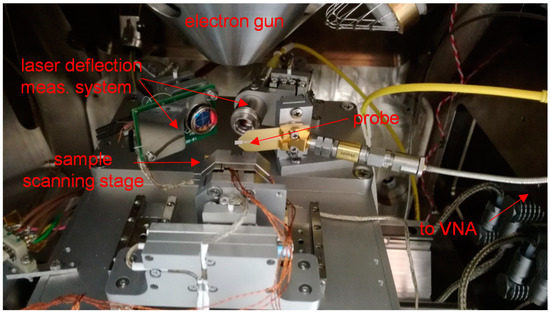
Figure 1.
Atomic force microscope (AFM)/scanning microwave microscopy (SMM) stage mounted in the SEM vacuum chamber. The AFM/SMM stage is built up with a sample scanning stage, a fixed microwave probe connected to the vector network analyzer (VNA) and a laser deflection system.
The radiofrequency scanning microscopy augmented up to 67 GHz uses a SMM cantilever consisting of a modified 25Pt300B microwave probe from Rocky Mountain Nanotechnology® (RMN) with a sub-100 nm apex radius (Figure 1). The probe has been redesigned to support a transverse electromagnetic mode (TEM) through a propagating microstrip structure. This new NSMM cantilever is fed by a coaxial cable connected to the microwave measurement system, i.e., the VNA. Consequently, a dedicated coaxial-to-microstrip transition built up with two parts was developed. In particular, the cantilever is embedded into a PCB waveguide structure that can be exchanged in the case of destroyed tips by using a solder-less PCB mount 1.85 mm connector from Rosenberger Corp. with a clamping and screwing mechanism.
Building hybrid scanning probe tools from scratch requires design considerations different from those conventionally found in single AFM. In contrast with conventional SEM used to image the sample surface, the objective here is to visualize the apex tip in contact with the sample. Consequently, the sample scanner is mounted vertically and parallel in respect to the electron beam of the SEM. The electron column occupies most of the space in the chamber and drastically limits the height of the AFM system. The system was designed to be as compact as possible to allow SEM operation during AFM/SMM measurements in the best conditions possible although observation with the highest resolution is not possible. It has to be noticed that the AFM/SMM stage is mounted on the chamber of the SEM compared to conventional stages fixed on the SEM door.
2.2. Traceability in the SMM Mode
In contrast to microwave-guided measurements, including a metallic waveguide, coaxial, on-wafer propagating structures for which the traceability has been established for decades, the normalization of SMM technology, including the experimental set-up and the measurement configuration and calibration standards, are still an issue. Whereas SMM technology has been identified as a unique solution to provide a microwave and millimeter-wave characterization at the submicron scale, there is an urgent need to harmonize the best practices at the international level. In particular, we identified the main bottlenecks to be tackled for offering quantitative and traceable SMM measurements. Firstly, whereas AFM can operate in air to provide a topography image of the sample under test, water meniscus in the vicinity of the apex tip of the probe contributes to the overall complex impedance at the apex tip, especially because water has a high dielectric constant and loss tangent in the microwave range. Moreover, the shape of the water meniscus is usually unknown; therefore, only approximations of the water meniscus can usually be derived by 3D electromagnetic modeling and are not easily discriminated from other parasitic capacitances involved in the measurement. Operating in a vacuum presents the advantage to allow the elimination of the water meniscus by heating the sample, simplifying the electrical modeling. Secondly, a second advantage of operating in an SEM is the possibility to directly image the probe in contact with the sample, even during the scanning operation. Indeed, probe microscopy tools, especially in the contact mode, are methods that may damage the sample or the tip apex with impacts on the electrical measurement, especially in the case of RF electrical measurements using sub-100 nm platinum/iridium wire as a sensing element. Finally, it is well accepted in the SMM community that spatial resolution is mainly governed by the apex tip geometry [36]. In particular, to surpass the diffraction limit imposed by the half-wavelength of radiation, waveguide structures with dimensions far below the wavelength of excitation exhibit evanescent electrical fields in the vicinity of the apex tip. Nevertheless, the collimation of the electrical fields is frequency dependent. Therefore, operating at a higher frequency improves the distribution of the electrical fields and the lateral resolution and, incidentally, the signal-to-noise ratio (SNR). To verify this assumption, electromagnetic simulations using a high-frequency structure simulator (HFSS) were performed at three test frequencies (1, 10 and 30 GHz) by designing an RMN probe and plotting the distribution of the electrical fields (the magnetic field here being negligible), as shown in Figure 2.
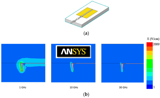
Figure 2.
(a) Rocky Mountain Nanotechnology® (RMN®) probe configuration. (b) High-frequency structure simulator (HFSS) simulation of the electrical field magnitude as a function of the frequency of operation. A 25Pt300B microwave probe from Rocky Mountain Nanotechnology® (RMN) consisting of an ultrasharp solid platinum wire tapered down to 100 nm and attached to a ceramic substrate (dielectric constant: 9.8) is designed in the ANSYS® HFSS.
As expected, the lateral resolution, i.e., the footprint of the electrical field distribution at the probe apex, decreases for higher frequencies. It has to be mentioned that the depth resolution is of course lower. These results are in favor of operating in the millimeter-wave regime. Nevertheless, as the transmission losses increase with frequency, especially in the RF cables and transitions from the input of the VNA to the AFM/SMM tip, there is a compromise between the lateral resolution and SNR. As an illustration, we present in Figure 3 the measured return loss measured up to 50 GHz of the probe. For frequencies greater than 35 GHz, the standing wave ratio is more pronounced, leading to a mixing of the amplitude and phase-shift of the complex reflection coefficient at the probe apex. It has to be mentioned that the measured response can be enhanced by considering the optimization of the mounting and soldering of the AFM/SMM probe on the PCB substrate, both done manually. In the following, we consider measurements performed at the test frequency of 30 GHz.
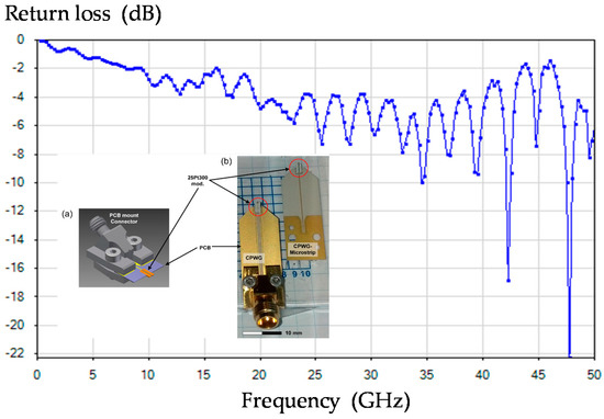
Figure 3.
Measured return loss of the AFM/SMM probe (including the modified RMN® cantilever, the PCB and the coaxial-to-PCB transition) in the input coaxial plane.
2.3. Reference Staircase Microcapacitor Sample
The electrical devices considered in this work are microsized metal oxide semiconductor (MOS) capacitors that have been widely studied by the metrology and research communities [38,39,40,41]. The MOS capacitors are composed of circular gold electrodes evaporated on silicon dioxide (SiO2) deposited on a highly doped P-type silicon substrate of resistivity 0.01 Ω.cm. The SEM image of the reference kit is depicted in Figure 4. In order to vary the capacitance values, the diameter of the upper gold pad diameter varies from 1 to 4 μm, and the SiO2 thickness ranges from 50 to 300 nm, with about 80 nm steps.
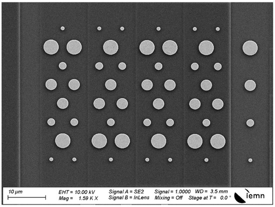
Figure 4.
SEM image of the metal oxide semiconductor (MOS) microcapacitor reference kit.
The reference kit is used for both calibration and verification. Prior to the measurements, the analytical derivation of the theoretical capacitances is considered. The impedance of the MOS structures measured at the tip apex of the probe is modeled by a series model consisting of an oxide capacitance Cox and a depletion capacitance Cdepl. Both capacitances can be described by the parallel plate capacitor formalism. The resulting capacitance CTOT is given by
The capacitance Cox is calculated from the areas of the gold pads A and the SiO2 thicknesses dox.
The silicon dioxide is assumed to have a relative dielectric constant of = 3.9. The charge stored on the capacitor is distributed across a certain depth that adds the depletion series capacitance Cdepl in series to Cox. The capacitance was estimated to be proportional to the area A of the metallic electrode and inversely proportional to the depleted zone depth ddepl according to
with and where = 12 is the relative permittivity of the silicon bulk substrate, Ψ represents the interface band bending at the Si/SiO2 interface and is set to 300 mV, q is the charge of the electron (1.6 × 10⁻¹⁹ C) and NA is the doping level of the silicon bulk around 5 × 10¹⁸/cm−3. Although the interface band bending at the interface is relatively unknown, due to the high doping, the depletion capacitance is higher than the oxide capacitance. Therefore, since the two capacitances are in series, an uncertainty on Ψ has a negligible effect on the total capacitance.
The calibration procedure consists of determining a two-port error terms box to convert the measured complex reflection coefficient ΓM by the VNA into the complex reflection Γ at the apex tip. Then, the calibration model established can be used to determine the other capacitance values. The one-port vector calibration method model used to make the link between the reflection coefficient ΓM measured by the VNA and the reflection coefficient Γ is given by
The complex terms , and correspond, respectively, to the directivity, source match and reflection tracking errors. These calibration parameters depend on the microwave path between the apex tip of the probe and VNA receivers. System (4) is resolved by a derived SOL calibration method that makes use of the measurements of the reflection coefficient ΓM1, ΓM2 and ΓM3 of three assumed reference loads, called load ZREF1 ZREF2 and ZREF3 with theoretical reflection coefficients Γ1, Γ2 and Γ3. Capacitors that have spaced capacitances values are ideally chosen on the desired range of capacitances to be measured.
3. Results
3.1. Measurement Configuration and Verification
The standard operation procedure (SOP) described here follows the material preparation presented in the previous section. First, we ensure a stable lab climate in a controlled environment (temperature, humidity) to enable the stable operation of the SMM with minimum mechanical and electrical drift. The measurements are performed at 30 GHz using a modified 25PT300A AFM tip from Rocky Mountain Nanotechnology®. A PNA Keysight® E8364B VNA with the RF power source set to 2 dBm and the intermediate frequency bandwidth (IFBW) to 50 Hz is used. Highly stable coaxial cables and feedthrough coaxial transitions are used to connect the VNA to the probe. Nanonis® Signal Conditioning (SC5) and Real-Time Controller (RC5) modules are used to drive the AFM measurements. The cantilever deflection voltage is set to 90 mV, the approach–retract factor is about 6 nm/mV and the resulting force is estimated to be 9.7 µN. The images were scanned over 40 × 40 μm2 with 256 pixels with a scanning time (forward and backward) of 5119 s. Prior to the measurement, SEM imaging of the apex tip is performed to check the tip shape (Figure 5a). Topography, together with both real and imaginary parts of the measured complex reflection coefficient ΓM images, is acquired simultaneously (Figure 5b,c).
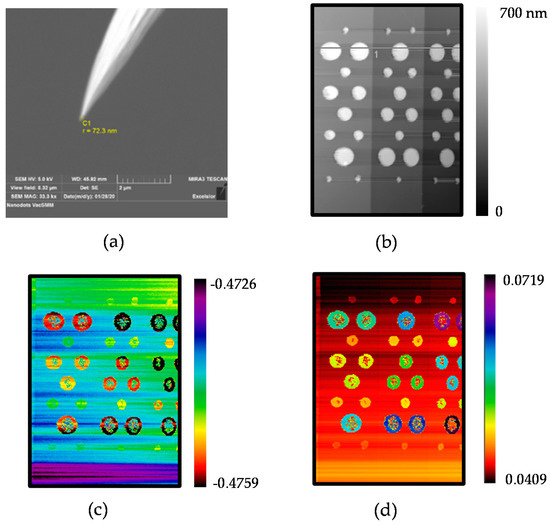
Figure 5.
(a) SEM image of the apex tip. (b) Measured atomic force microscopy image, (c) real part and (d) imaginary part images of the complex reflection coefficient ΓM: f = 30 GHz. (Only the parts of the images of interest are represented on a 25 × 35 µm2 area).
We keep raw data (Nanonis® *.sxm format) and postprocess data separate and make sure to not overwrite raw data during analysis treatment, presented in the following sub-section.
3.2. Data Analysis
The raw data are transferred to Gwyddion® software for analysis. We cross-check the images from Figure 5 together. Then, each capacitor on the atomic force microscopy image in Figure 5b is referenced according to Figure 6.
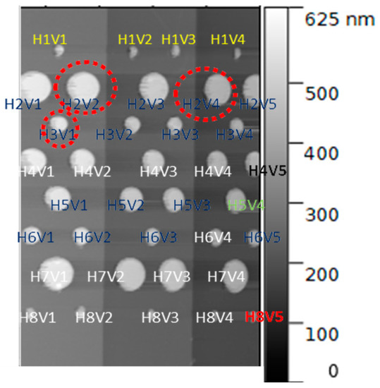
Figure 6.
Topography image with the named capacitor (for example, H2V1 corresponds to horizontal Position 2 and Vertical Position 1). The red circles denote the capacitors used for calibration.
From the topography image given in Figure 6, we can calculate the theoretical capacitances according to Relations (2) to (3). The four circular areas of the metallic electrodes have targeted diameters of 1, 2, 3 and 4 µm, respectively. The three oxide layers determined from the topography image by considering the 1D profile (indicated in Line 1 in Figure 5b) are, respectively, 87.5, 137.1 and 198.3 nm. The corresponding oxide capacitances have values in the range of 0.14–5.09 fF (10−15 F). It has to be mentioned that MC2 Technologies® has developed two reference calibration kits considering doped P-type silicon with substrate resistivity of 1 and 0.01 Ω.cm, respectively. In contrast with our previous studies based on the first type of reference capacitance kit, due to the high doping of the silicon substrate, the depletion capacitance is negligible (fifth row of Table 1). Consequently, it is highly recommended to consider highly doped materials for the fabrication of the MOS capacitance kit. Another possibility investigated in [21] is to consider indium tin oxide (ITO) as the metal substrate. From the theoretical capacitance values, the theoretical reflection coefficient Γ of the capacitors is calculated. The capacitors considered lossless (as demonstrated in Section 2) have phase-shifts of Γ in the range −0.15–−5.31 degrees.

Table 1.
Theoretical capacitances and phase-shifts of Γ at 30 GHz determined from the AFM topography image (H2V2, H2V4 and H3V1 denoted * are used for calibration) and relative error between total capacitance and oxide capacitance values.
The calibration process developed in Section 2.3 is applied by considering three oxide capacitances values as the reference loads. From Table 1, we chose H2V2, H2V4 and H3V1 with capacitances 0.56, 2.24 and 5.09 fF to cover a wide range of capacitance values. As the calibrated measurements are very sensitive to the knowledge of the reference loads, we did not consider the smallest capacitances as reference. Using Equation (4), the complex error terms , and are determined (Table 2).
Table 2.
Calibration error terms obtained from the modified SOL calibration procedure. f = 30 GHz.
Whereas in conventional guided measurements, the directivity corresponds to a small incident signal that leaks through the forward path of the coupler and into the receiver of the VNA, the directivity around −6.68 dB corresponds mainly to mismatch effects in the path of the microstrip probe without reflecting off the device under test (DUT). Given the nature of the probe structure for which the end platinum wire of the cantilever is not supported by a TEM propagating mode, around 75% of the incident power is transmitted to the DUT. The reflection tracking around −32 dB indicates transmission losses from the apex tip to the VNA receiver of around 16 dB. From Figure 3, 3 dB transmission losses are attributed to the microwave probe, including the coaxial-to-microstrip transition. Consequently, the transmission losses around 13 dB are attributed to the coaxial cables and transition (vacuum coaxial transition at the air/SEM interface). The input power and the IFBW set to 0 dBm and 50 Hz, respectively, are therefore appropriate for accurate measurements. Ideally, in reflection measurements, all of the signal that is reflected off of the DUT is measured at the VNA receiver. Due to the high impedance of the probe apex in contrast with the 50 Ω impedance of the microwave instrumentation (including the microstrip part of the probe, coaxial-to-microstrip transition, coaxial cables and feedthrough, VNA), a large part of the signal reflects off the DUT, and multiple internal reflections occur between the probe apex and the DUT. In particular, the source match value of −0.87 dB indicates that 80% of the microwave power is reflected off the DUT. All of these systematic errors are taken into account by the calibration procedure. By inverting Relationship (5), the calibrated complex reflection coefficient Γ in the reference plane of the apex tip can be determined.
We developed a MATLAB® program called “SPAR2Y’ for the determination of the inverse problem, i.e., determination of the quantitative data from the measured complex reflection coefficient (Figure 7). The input variables of the program consist of real and imaginary parts of ΓM,ij, the error terms e00, e11, e10e01 and the test frequency to derive the data of interest in a text file format.
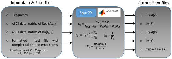
Figure 7.
Functional diagram of the MATLAB® script developed for quantitative data determination. The input data file *.txt consists of the frequency of operation, measured real and imaginary parts of the complex reflection coefficient ΓM,ij and complex calibration error terms. The code Spar2Y determines the calibrated complex reflection coefficient Γij at the probe tip and the related complex impedance Zij admittance Yij (including capacitance Cij). An output *.txt file is generated.
After running the program “SPAR2Y,” we present the images of the real part and imaginary part of the admittance Y obtained after calibration (Figure 8). In addition, we plot a 1D profile along the x-axis to appreciate the fluctuations.
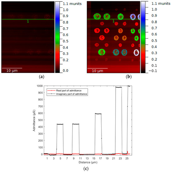
Figure 8.
(a) Real part and (b) imaginary part images of the admittance Y measured at 30 GHz. (c) Extracted 1D profile along the x-axis (from Line 1 denoted in (a,b)).
The image of the microwave conductance indicates a value close to 0, demonstrating that the DUT is only reactive. The extracted 1D profile given in Figure 8c indicates the insensitivity of the real part of the admittance along the x-distance. Figure 8b shows the imaginary part of the admittance that is a direct signature of the capacitance image. Along the 1D profile, the signal fluctuations are very low. Nevertheless, most of the DUTs show heterogeneity in the middle of their respective areas. Investigations were made to identify the origin. In particular, a fine analysis of the topography, microwave and SEM images lead to the conclusion that contamination effects mainly on the middle of the gold patch areas induce a reduction or loss of electrical contact between the apex tip and the gold patch. From the imaginary part image of Y, the capacitance image at 30 GHz is plotted in a 3D format in Figure 9.
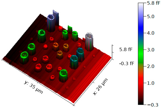
Figure 9.
Three-dimensional (3D) capacitance image of the reference kit measured at 30 GHz.
From Figure 9, the microwave capacitances are extracted. To quantify the error between theoretical and microwave capacitances, we present in Figure 10 the relative error between the two types of data after removing the reference capacitors used for calibration and erroneous microwave data (probe tip non contacting the DUT).
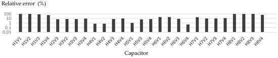
Figure 10.
Relative error (in log scale) in the determination of the microwave capacitance at 30 GHz.
From Figure 10, we demonstrate that the smallest MOS capacitance values present errors reaching 100%. The main reason is that the measurement accuracy depends on the reference devices used for the calibration. The smallest capacitances have not been considered in this study to focus mainly on capacitors whose measurements present a good signal-to-noise (SNR) ratio. Indeed, in contrast with capacitances values greater than 300 aF, those capacitors exhibit large relative fluctuations in the observed microwave signals. Further complicating this, the drift of the microwave signal observed in the Y scanning direction (see Figure 5d) has more impact on the determination of the smallest capacitances as they are physically positioned at the beginning and end of the scanning area. Further discussion on this point is proposed in the following section. For all other capacitors (>300 aF), the relative error reaches a maximum value of 20%, with a median value of 8.7%.
In the following section, we analyze the capacitance fluctuation considering a straight 1D profile as presented in Figure 11a (non calibrated topography). In particular, we focus on the smallest capacitors related to the probe tip directly in contact with the silicon oxide layer. Figure 11b shows a zoomed-in version of Figure 11a in the x-range of 17–25 µm. Two steps of silicon oxide with absolute thicknesses of 198.3 and 137.1 nm are identified. The related extracted microwave capacitance profile demonstrates that the corresponding capacitances are about 40 and 22 aF, respectively, with fluctuations of about ±5 aF.
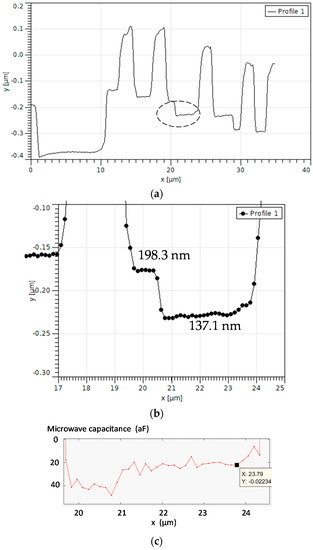
Figure 11.
Relative error in the determination of the microwave capacitance at 30 GHz. (a) Non calibrated topography 1D profile. (b) Topography 1D profile in the range of 17–25 µm. (c) Extracted 1D microwave capacitance on the silicon oxide steps.
4. Conclusion
Calibrated capacitances values in the millimeter-wave regime considering a frequency of operation of 30 GHz (free-space wavelength of 1 mm) have been presented. The scanning probe instrumentation proposed built entirely from scratch is based on a combined AFM/SMM integrated inside an SEM. The stability of the microwave path is ensured by keeping the microwave probe and cables fixed during the scanning operation. Only the sample under test is moved under the probe. A high signal-to-noise ratio is obtained by choosing appropriate electrical parameters for the VNA, i.e., the RF power set to 0 dBm and IFBW to 50 Hz. No external electrical matching network commonly found in SMM set-ups is used. Instead, we increased the frequency of operation up to 30 GHz to obtain a good compromise between the collimation of the electrical fields in the vicinity of the tip apex and moderate losses in the microwave path between the microwave source and the apex tip. We focused mainly on MOS capacitors whose theoretical values are in the range of 0.5–5 fF. A dedicated calibration is developed to extract the capacitances values with a median error of 10%. To that end, a dedicated standard operation procedure, including the measurement protocol and data analysis, is used to derive the quantitative data of interest. The measurement performance is demonstrated with capacitance fluctuations in the order of ±5 aF.
5. Discussion
These results are very instructive and lay the background for future microwave nanometrology. Indeed, SMM techniques have become a mature technology in both academic and industrial laboratories. National metrology institutes have considerably contributed to enhancing SMM technology. In this effort, we analyzed the experimental results presented in this work, and we draw conclusions for future works in the following.
- −
- The theoretical capacitances do not consider fringing field effects. Future works will include analytical and electromagnetic simulations to derive more realistic values of capacitance values. In addition, the coupling effect from neighboring capacitors will be studied to yield the optimization of the disposition of the capacitors.
- −
- Electrical drift of the microwave instrumentation is inevitable. Although its impact is reduced for capacitances greater than 300 aF, there is an urgent need to introduce solutions to achieve stable measurements for capacitance as low as 1 aF. To tackle this issue, the microwave path must be reduced to the minimum. The research direction should be directed towards the implementation of the microwave instrumentation closest to the probe. In particular, we omitted capacitances below 300 aF as the longitudinal drift (along the y-axis) is not compatible with accurate extraction of the electrical parameters. To complicate, the reference kit is used with the smallest capacitors on the top and on the back of the scanning area. It is highly recommended to design reference kits by taking into consideration the electrical drift. In other words, the scanning area and in particular the scanning time must be reduced as necessary to yield consistent quantitative data.
- −
- The calibration reference kit in this study is based on microsized capacitors. Decreasing the size of the microcapacitors is still an issue to address nanoscale characterization. Indeed, the apex tip must be reduced to accommodate smaller footprints. In this effort, we considered a relatively small apex radius of 70 nm. The size can be further reduced as an apex size below 20 nm is commercially available. Operating inside a SEM is beneficial to limit the scanning area when fragile sub-20 nm apex sizes are considered. Ongoing works related to the free-space calibration procedure that exploits the stand-off between the tip apex and the material surface is also a possible alternative. The instrumentation proposed offers the unique possibility to image the apex geometry and to record simultaneously the microwave signals. Indeed, the apex geometry is the main factor that governs the theoretical derivation of the coupling capacitance.
Author Contributions
Conceptualization, K.H., D.T.; methodology, P.P., D.T., C.L., D.D., S.E., C.B., G.D. and K.H.; software, P.P., D.T., C.L., D.D., S.E., C.B., G.D. and K.H.; validation, P.P., D.T., C.L., D.D., S.E., C.B., G.D. and K.H.; formal analysis, P.P., D.D. and K.H.; data curation, P.P., D.D. and K.H.; writing—original draft preparation, P.P., D.D. and K.H.; writing—review and editing, P.P., D.D. and K.H.; supervision, D.T. and K.H.; project administration, K.H.; funding acquisition, D.T., G.D. and K.H. All authors have read and agreed to the published version of the manuscript.
Funding
This work has received funding from the European Union Horizon H2020 Programme (H2020-NMBP07-2017) under grant agreement n°761036 MMAMA. This work used the facilities within the EQPX ExCELSiOR funded by the National Research Agency (ANR).
Data Availability Statement
The data presented in this study are available on request from the corresponding author.
Conflicts of Interest
The authors declare no conflict of interest
References
- Ghodgaonkar, D.K.; Varadan, V.V.; Varadan, V.K. A free-space method for measurement of dielectric constants and loss tangents at microwave frequencies. IEEE Trans. Instrum. Meas. 1989, 38, 789–793. [Google Scholar] [CrossRef]
- Haddadi, K.; Lasri, T. Geometrical optics-based model for dielectric constant and loss tangent free-space measurement. IEEE Trans. Instrum. Meas. 2014, 63, 1818–1823. [Google Scholar] [CrossRef]
- Koutsoukis, G.; Alic, I.; Vavouliotis, A.; Kienberger, F.; Haddadi, K. Roll-to-Roll In-Line Implementation of Microwave Free-Space Non-Destructive Evaluation of Conductive Composite Thin Layer Materials. Appl. Sci. 2021, 11, 378. [Google Scholar] [CrossRef]
- Arz, U.; Probst, T.; Kuhlmann, K.; Ridler, N.; Shang, X.; Mubarak, F.; Hoffmann, J.; Wollensack, M.; Zeier, M.; Phung, G.N.; et al. Best Practice Guide for Planar S-Parameter Measurements Using Vector Network Analysers; Physikalisch-Technische Bundesanstalt (PTB): Braunschweig, Germany, 2019. [Google Scholar]
- Misra, D.K. A quasi-static analysis of open-ended coaxial lines (short paper). IEEE Trans. Microw. Theory Tech. 1987, 35, 925–928. [Google Scholar] [CrossRef]
- Bakli, H.; Haddadi, K. Microwave interferometry based on open-ended coaxial technique for high sensitivity liquid sensing. Adv. Electromagn. 2017, 6, 88–93. [Google Scholar] [CrossRef]
- Bakli, H.; Haddadi, K. Quantitative determination of small dielectric and loss tangent contrasts in liquids. In Proceedings of the 2017 IEEE International Instrumentation and Measurement Technology Conference (I2MTC), Turin, Italy, 22–25 May 2017; pp. 1–6. [Google Scholar]
- Krupka, J.; Derzakowski, K.; Riddle, B.; Baker-Jarvis, J. A dielectric resonator for measurements of complex permittivity of low loss dielectric materials as a function of temperature. Meas. Sci. Technol. 1998, 9, 1751. [Google Scholar] [CrossRef]
- Synge, E.H. XXXVIII. A suggested method for extending microscopic resolution into the ultra-microscopic region. Lond. Edinb. Dublin Philos. Mag. J. Sci. 1928, 6, 356–362. [Google Scholar] [CrossRef]
- Ash, E.A.; Nicholls, G. Super-resolution aperture scanning microscope. Nature 1972, 237, 510–512. [Google Scholar] [CrossRef]
- Anlage, S.M.; Talanov, V.V.; Schwartz, A.R. Principles of near-field microwave microscopy. In Scanning Probe Microscopy; Springer: New York, NY, USA, 2007; pp. 215–253. [Google Scholar]
- Imtiaz, A.; Wallis, T.M.; Kabos, P. Near-field scanning microwave microscopy: An emerging research tool for nanoscale metrology. IEEE Microw. Mag. 2014, 15, 52–64. [Google Scholar] [CrossRef]
- Plassard, C.; Bourillot, E.; Rossignol, J.; Lacroute, Y.; Lepleux, E.; Pacheco, L.; Lesniewska, E. Detection of defects buried in metallic samples by scanning microwave microscopy. Phys. Rev. B 2011, 83, 121409. [Google Scholar] [CrossRef]
- Gramse, G.; Kasper, M.; Fumagalli, L.; Gomila, G.; Hinterdorfer, P.; Kienberger, F. Calibrated complex impedance and permittivity measurements with scanning microwave microscopy. Nanotechnology 2014, 25, 145703. [Google Scholar] [CrossRef]
- Fabiani, S.; Mencarelli, D.; Di Donato, A.; Monti, T.; Venanzoni, G.; Morini, A.; Rozzi, T.; Farina, M. Broadband scanning microwave microscopy investigation of graphene. In Proceedings of the 2011 IEEE MTT-S International Microwave Symposium, Baltimore, MD, USA, 5–10 June 2011; pp. 1–4. [Google Scholar]
- Buchter, A.; Hoffmann, J.; Delvallée, A.; Brinciotti, E.; Hapiuk, D.; Licitra, C.; Louarn, K.; Arnoult, A.; Almuneau, G.; Piquemal, F.; et al. Scanning microwave microscopy applied to semiconducting GaAs structures. Rev. Sci. Instrum. 2018, 89, 023704. [Google Scholar] [CrossRef]
- Dargent, T.; Haddadi, K.; Lasri, T.; Clément, N.; Ducatteau, D.; Legrand, B.; Tanbakuchi, H.; Theron, D. An interferometric scanning microwave microscope and calibration method for sub-fF microwave measurements. Rev. Sci. Instrum. 2013, 84, 123705. [Google Scholar] [CrossRef]
- Biagi, M.C.; Fabregas, R.; Gramse, G.; Van Der Hofstadt, M.; Juárez, A.; Kienberger, F.; Fumagalli, L.; Gomila, G. Nanoscale electric permittivity of single bacterial cells at gigahertz frequencies by scanning microwave microscopy. ACS Nano 2016, 10, 280–288. [Google Scholar] [CrossRef]
- Farina, M.; Di Donato, A.; Mencarelli, D.; Venanzoni, G.; Morini, A. High resolution scanning microwave microscopy for applications in liquid environment. IEEE Microw. Wirel. Compon. Lett. 2012, 22, 595–597. [Google Scholar] [CrossRef]
- Farina, M.; Hwang, J.C. Scanning Microwave Microscopy for Biological Applications: Introducing the State of the Art and Inverted SMM. IEEE Microw. Mag. 2020, 21, 52–59. [Google Scholar] [CrossRef]
- Ren, D.; Nemati, Z.; Lee, C.H.; Li, J.; Haddadi, K.; Wallace, D.C.; Burke, P.J. An ultra-high bandwidth nano-electronic interface to the interior of living cells with integrated fluorescence readout of metabolic activity. Sci. Rep. 2020, 10, 1–12. [Google Scholar] [CrossRef] [PubMed]
- Li, J.; Nemati, Z.; Haddadi, K.; Wallace, D.C.; Burke, P.J. Scanning microwave microscopy of vital mitochondria in respiration buffer. In Proceedings of the 2018 IEEE/MTT-S International Microwave Symposium-IMS, Philadelphia, PA, USA, 10–15 June 2018; pp. 115–118. [Google Scholar]
- Tselev, A.; Velmurugan, J.; Ievlev, A.V.; Kalinin, S.V.; Kolmakov, A. Seeing through walls at the nanoscale: Microwave microscopy of enclosed objects and processes in liquids. ACS Nano 2016, 10, 3562–3570. [Google Scholar] [CrossRef] [PubMed]
- Haddadi, K.; Gu, S.; Lasri, T. Sensing of liquid droplets with a scanning near-field microwave microscope. Sens. Actuators A Phys. 2015, 230, 170–174. [Google Scholar] [CrossRef]
- Kim, S.; Yoo, H.; Lee, K.; Friedman, B.; Gaspar, M.A.; Levicky, R. Distance control for a near-field scanning microwave microscope in liquid using a quartz tuning fork. Appl. Phys. Lett. 2005, 86, 153506. [Google Scholar] [CrossRef]
- Geaney, S.; Cox, D.; Hönigl-Decrinis, T.; Shaikhaidarov, R.; Kubatkin, S.E.; Lindström, T.; Danilov, A.V.; de Graaf, S.E. Near-field Scanning Microwave Microscopy in the Single photon Regime. Sci. Rep. 2019, 9, 1–7. [Google Scholar] [CrossRef]
- Rubin, K.A.; Yang, Y.; Amster, O.; Scrymgeour, D.A.; Misra, S. Scanning Microwave Impedance Microscopy (sMIM) in Electronic and Quantum Materials. In Electrical Atomic Force Microscopy for Nanoelectronics; Springer: Cham, Switzerland, 2019; pp. 385–408. [Google Scholar]
- Shi, Y.; Kahn, J.; Niu, B.; Fei, Z.; Sun, B.; Cai, X.; Francisco, B.A.; Wu, D.; Shen, Z.X.; Xu, X.; et al. Imaging quantum spin Hall edges in monolayer WTe2. Sci. Adv. 2019, 5, eaat8799. [Google Scholar] [CrossRef] [PubMed]
- Seabron, E.; MacLaren, S.; Xie, X.; Rotkin, S.V.; Rogers, J.A.; Wilson, W.L. Scanning probe microwave reflectivity of aligned single-walled carbon nanotubes: Imaging of electronic structure and quantum behavior at the nanoscale. ACS Nano 2016, 10, 360–368. [Google Scholar] [CrossRef]
- Gramse, G.; Kölker, A.; Škereň, T.; Stock, T.J.; Aeppli, G.; Kienberger, F.; Fuhrer, A.; Curson, N.J. Nanoscale imaging of mobile carriers and trapped charges in delta doped silicon p–n junctions. Nat. Electron. 2020, 3, 531–538. [Google Scholar] [CrossRef]
- Hovsepyan, A.; Babajanyan, A.; Sargsyan, T.; Melikyan, H.; Kim, S.; Kim, J.; Lee, K.; Friedman, B. Direct imaging of photoconductivity of solar cells by using a near-field scanning microwave microprobe. J. Appl. Phys. 2009, 106, 114901. [Google Scholar] [CrossRef]
- Weber, J.C.; Schlager, J.B.; Sanford, N.A.; Imtiaz, A.; Wallis, T.M.; Mansfield, L.M.; Coakley, K.J.; Bertness, K.A.; Kabos, P.; Bright, V.M. A near-field scanning microwave microscope for characterization of inhomogeneous photovoltaics. Rev. Sci. Instrum. 2012, 83, 083702. [Google Scholar] [CrossRef] [PubMed]
- Berweger, S.; MacDonald, G.A.; Yang, M.; Coakley, K.J.; Berry, J.J.; Zhu, K.; DelRio, F.W.; Wallis, T.M.; Kabos, P. Electronic and morphological inhomogeneities in pristine and deteriorated perovskite photovoltaic films. Nano Lett. 2017, 17, 1796–1801. [Google Scholar] [CrossRef]
- Haddadi, K.; Haenssler, O.C.; Daffe, K.; Eliet, S.; Boyaval, C.; Theron, D.; Dambrine, G. Combined scanning microwave and electron microscopy: A novel toolbox for hybrid nanoscale material analysis. In Proceedings of the 2017 IEEE MTT-S International Microwave Workshop Series on Advanced Materials and Processes for RF and THz Applications (IMWS-AMP), Pavia, Italy, 20–22 September 2017; pp. 1–3. [Google Scholar]
- Haddadi, K.; Haenssler, O.C.; Boyaval, C.; Theron, D.; Dambrine, G. Near-field scanning millimeter-wave microscope combined with a scanning electron microscope. In Proceedings of the 2017 IEEE MTT-S International Microwave Symposium (IMS), Honolulu, HI, USA, 4–9 June 2017; pp. 1656–1659. [Google Scholar]
- Polovodov, P.; Brillard, C.; Haenssler, O.C.; Boyaval, C.; Deresmes, D.; Eliet, S.; Wang, F.; Clément, N.; Théron, D.; Dambrine, G.; et al. Electromagnetic Modeling in Near-Field Scanning Microwave Microscopy Highlighting Limitations in Spatial and Electrical Resolutions. In Proceedings of the 2018 IEEE MTT-S International Conference on Numerical Electromagnetic and Multiphysics Modeling and Optimization (NEMO), Reykjavik, Iceland, 8–10 August 2018; pp. 1–4. [Google Scholar]
- Polovodov, P.; Théron, D.; Eliet, S.; Avramovic, V.; Boyaval, C.; Deresmes, D.; Dambrine, G.; Haddadi, K. Operation of Near-Field Scanning Millimeter-wave Microscopy up to 67 GHz under Scanning Electron Microscopy Vision. In Proceedings of the 2020 IEEE/MTT-S International Microwave Symposium (IMS), Los Angeles, CA, USA, 4–6 August 2020; pp. 95–98. [Google Scholar]
- Kasper, M.; Gramse, G.; Hoffmann, J.; Gaquiere, C.; Feger, R.; Stelzer, A.; Smoliner, J.; Kienberger, F. Metal-oxide-semiconductor capacitors and Schottky diodes studied with scanning microwave microscopy at 18 GHz. J. Appl. Phys. 2014, 116, 184301. [Google Scholar] [CrossRef]
- Haddadi, K.; Brillard, C.; Dambrine, G.; Théron, D. Sensitivity and accuracy analysis in scanning microwave microscopy. In Proceedings of the 2016 IEEE MTT-S International Microwave Symposium (IMS), San Francisco, CA, USA, 22–27 May 2016; pp. 1–4. [Google Scholar]
- Haddadi, K.; Polovodov, P.; Théron, D.; Dambrine, G. Quantitative Error Analysis in Near-Field Scanning Microwave Microscopy. In Proceedings of the 2018 International Conference on Manipulation, Automation and Robotics at Small Scales (MARSS), Nagoya, Japan, 4–8 July 2018; pp. 1–6. [Google Scholar]
- Morán-Meza, J.A.; Delvallée, A.; Allal, D.; Piquemal, F. A substitution method for nanoscale capacitance calibration using scanning microwave microscopy. Meas. Sci. Technol. 2020, 31, 074009. [Google Scholar] [CrossRef]
Publisher’s Note: MDPI stays neutral with regard to jurisdictional claims in published maps and institutional affiliations. |
© 2021 by the authors. Licensee MDPI, Basel, Switzerland. This article is an open access article distributed under the terms and conditions of the Creative Commons Attribution (CC BY) license (http://creativecommons.org/licenses/by/4.0/).