
Epitaxial Graphene on 4H-SiC (0001) as a Versatile Platform for Materials Growth: Mini-Review


Abstract
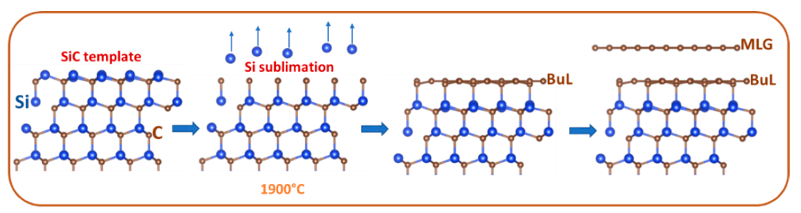
:1. Introduction
2. Key Properties of Epitaxial Graphene as a Substrate for Materials Deposition
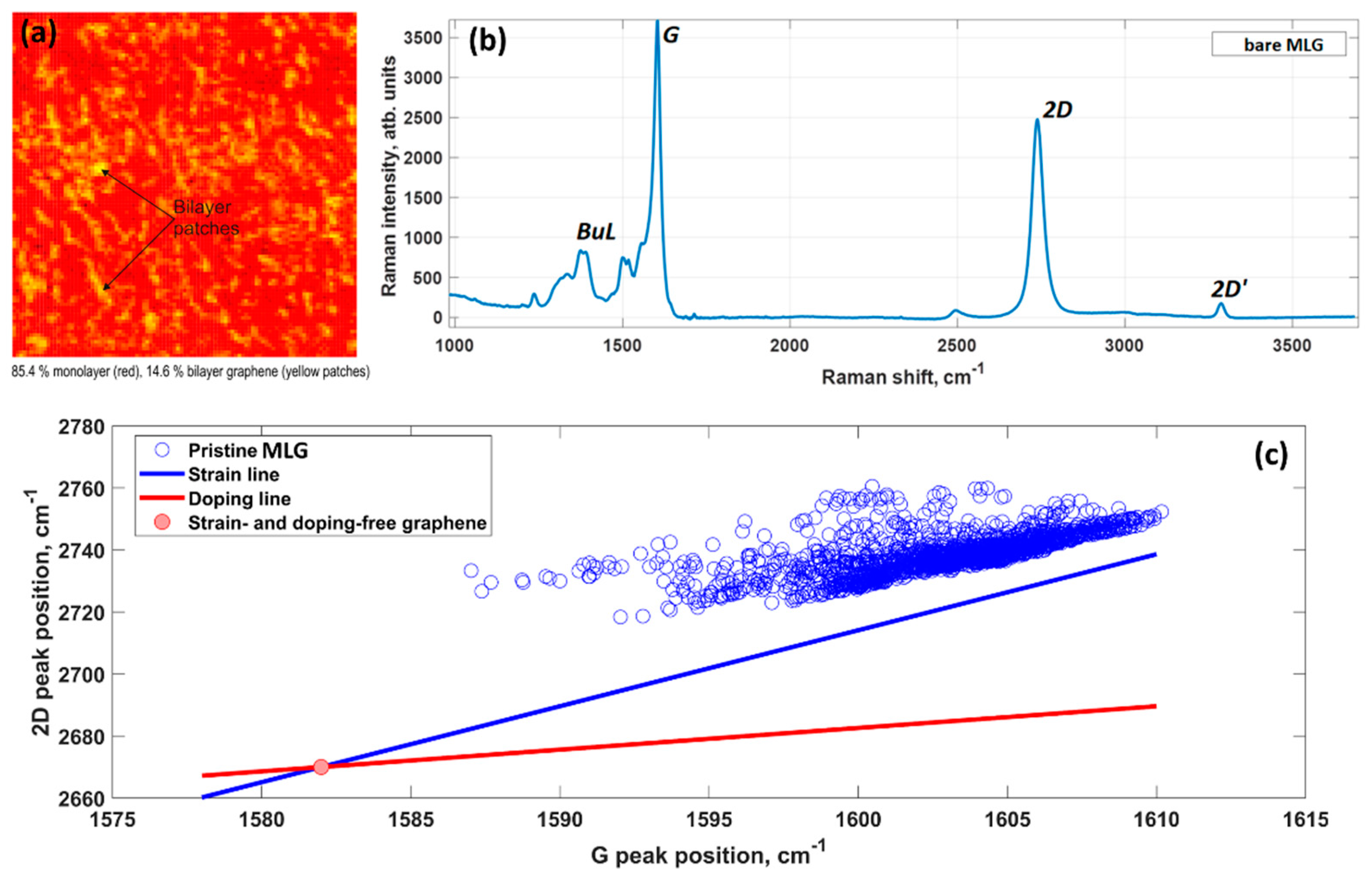
- (a)
- Step edges. Graphene on SiC has terrace-stepped morphology. Adsorption of atomic species on the steps edges is expected to be much stronger than on terraces.
- (b)
- Charge-unbalanced electron-hole puddles. The supporting SiC substrate is responsible not only for the doping of graphene but also for the appearance of charge density fluctuations. Randomly distributed negatively and positively charged regions may favor increased adsorption and nucleation rate.
- (c)
- Strained regions. Compressive or tensile strain leading to alteration of orbital hybridization and substrate-induced strain fluctuations are considered as another important factor determining an increased reactivity of epitaxial graphene compared to exfoliated graphene.
- (d)
- Edges of the bilayer graphene inclusions. Since as-grown monolayer epitaxial graphene usually includes nanoscale overgrown areas related to bilayer graphene, it is reasonable to assume that unsaturated edges of these inclusions may create extra nucleation sites.
3. Deposition of Noble Metals on Epitaxial Graphene/4H-SiC by dc Magnetron Sputtering
4. Deposition of Metals (Copper, Lead, Mercury, Lithium) on Epitaxial Graphene/4H-SiC by Electroplating
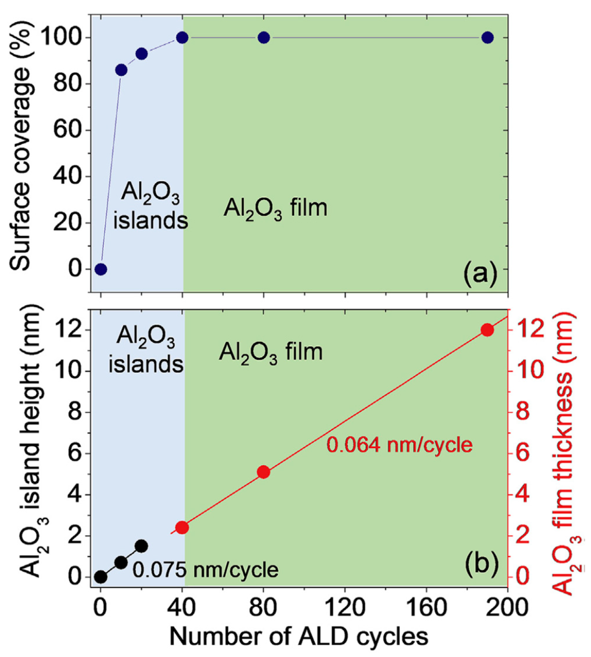
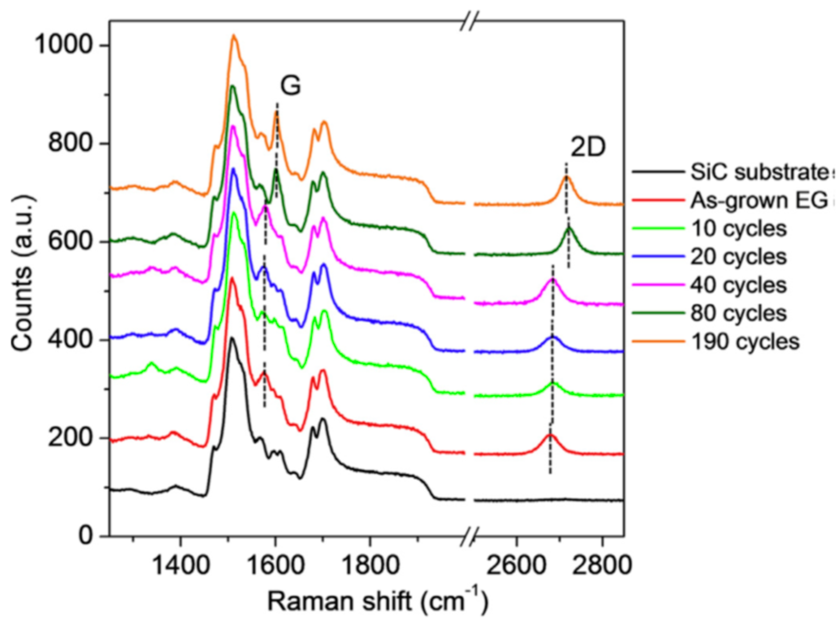
5. Atomic Layer Deposition of Insulators on Epitaxial Graphene
6. Concluding Remarks
Author Contributions
Funding
Institutional Review Board Statement
Informed Consent Statement
Data Availability Statement
Acknowledgments
Conflicts of Interest
References
- Virojanadara, C.; Syväjarvi, M.; Yakimova, R.; Johansson, L.I.; Zakharov, A.A.; Balasubramanian, T. Homogeneous large-area graphene layer growth on 6H-SiC(0001). Phys. Rev. B 2008, 78, 245403. [Google Scholar] [CrossRef]
- Tzalenchuk, A.; Lara-Avila, S.; Kalaboukhov, A.; Paolillo, S.; Syväjärvi, M.; Yakimova, R.; Kazakova, O.; Janssen, T.J.B.M.; Fal’ko, V.; Kubatkin, S. Towards a quantum resistance standard based on epitaxial graphene. Nat. Nanotechnol. 2010, 5, 186–189. [Google Scholar] [CrossRef]
- Janssen, T.J.B.M.; Rozhko, S.; Antonov, I.; Tzalenchuk, A.; Williams, J.M.; Melhem, Z.; He, H.; Lara-Avila, S.; Kubatkin, S.; Yakimova, R. Operation of graphene quantum Hall resistance standard in a cryogen-free table-top system. 2D Mater. 2015, 2, 035015. [Google Scholar] [CrossRef] [Green Version]
- Lartsev, A.; Lara-Avila, S.; Danilov, A.; Kubatkin, S.; Tzalenchuk, A.; Yakimova, R. A prototype of RK/200 quantum Hall array resistance standard on epitaxial graphene. J. Appl. Phys. 2015, 118, 044506. [Google Scholar] [CrossRef] [Green Version]
- Alexander-Webber, J.A.; Baker, A.M.R.; Janssen, T.J.B.M.; Tzalenchuk, A.; Lara-Avila, S.; Kubatkin, S.; Yakimova, R.; Piot, B.A.; Maude, D.K.; Nicholas, R.J. Phase Space for the Breakdown of the Quantum Hall Effect in Epitaxial Graphene. Phys. Rev. Lett. 2013, 111, 096601. [Google Scholar] [CrossRef] [PubMed] [Green Version]
- Rodner, M.; Bahonjic, J.; Mathisen, M.; Gunnarsson, R.; Ekeroth, S.; Helmersson, U.; Ivanov, I.G.; Yakimova, R.; Eriksson, J. Performance tuning of gas sensors based on epitaxial graphene on silicon carbide. Mater. Des. 2018, 153, 153–158. [Google Scholar] [CrossRef]
- Eriksson, J.; Puglisi, D.; Kang, Y.H.; Yakimova, R.; Lloyd Spetz, A. Adjusting the electronic properties and gas reactivity of epitaxial graphene by thin surface metallization. Phys. B 2014, 439, 105–108. [Google Scholar] [CrossRef] [Green Version]
- Kruskopf, M.; Pakdehi, D.M.; Pierz, K.; Wundrack, S.; Stosch, R.; Dziomba, T.; Götz, M.; Baringhaus, J.; Aprojanz, J.; Tegenkamp, C.; et al. Comeback of epitaxial graphene for electronics: Large-area growth of bilayer-free graphene on SiC. 2D Mater. 2016, 3, 041002. [Google Scholar] [CrossRef]
- Shtepliuk, I.; Khranovskyy, V.; Yakimova, R. Combining graphene with silicon carbide: Synthesis and properties—A review, Semicond. Sci. Technol. 2016, 31, 113004. [Google Scholar] [CrossRef] [Green Version]
- Shtepliuk, I.; Iakimov, T.; Khranovskyy, V.; Eriksson, J.; Giannazzo, F.; Yakimova, R. Role of the Potential Barrier in the Electrical Performance of the Graphene/SiC Interface. Crystals 2017, 7, 162. [Google Scholar] [CrossRef] [Green Version]
- Yu, C.; Liu, Q.; He, Z.; Gao, X.; Wu, E.; Guo, J.; Zhou, C.; Feng, Z. Epitaxial graphene gas sensors on SiC substrate with high sensitivity. J. Semicond. 2020, 41, 032101. [Google Scholar] [CrossRef]
- Pearce, R.; Iakimov, T.; Andersson, M.; Hultman, L.; Lloyd Spetz, A.; Yakimova, R. Epitaxially grown graphene based gas sensors for ultra sensitive NO(2) detection. Sens. Actuators B 2011, 2, 451–455. [Google Scholar] [CrossRef] [Green Version]
- Melios, C.; Panchal, V.; Edmonds, K.; Lartsev, A.; Yakimova, R.; Kazakova, O. Detection of Ultralow Concentration NO2 in Complex Environment Using Epitaxial Graphene Sensors. ACS Sens. 2018, 3, 1666–1674. [Google Scholar] [CrossRef] [Green Version]
- Nagareddy, V.K.; Chan, H.K.; Hernández, S.C.; Wheeler, V.D.; Myers-Ward, R.L.; Nyakiti, L.O.; Eddy Jr., C.R.; Walton, S.G.; Goss, J.P.; Wright, N.G.; et al. Detection of polar chemical vapors using epitaxial graphene grown on SiC (0001). Appl. Phys. Lett. 2013, 102, 173103. [Google Scholar] [CrossRef]
- Melios, C.; Winters, M.; Strupiński, W.; Panchal, V.; Giusca, C.E.; Imalka Jayawardena, K.D.G.; Rorsman, N.; Ravi P. Silva, S.; Kazakova, O. Tuning epitaxial graphene sensitivity to water by hydrogen intercalation. Nanoscale 2017, 9, 3440–3448. [Google Scholar] [CrossRef] [PubMed] [Green Version]
- Nagareddy, V.K.; Gaskill, D.K.; Tedesco, J.L.; Myers-Ward, R.L.; Eddy, C.R., Jr.; Goss, J.P.; Wright, N.G.; Horsfall, A.B. Temperature dependent chemical sensitivity of epitaxial graphene. Mater. Sci. Forum 2012, 717–720, 691–694. [Google Scholar] [CrossRef]
- Panchal, V.; Cedergren, K.; Yakimova, R.; Tzalenchuk, A.; Kubatkin, S.; Kazakova, O. Small epitaxial graphene devices for magnetosensing applications. J. Appl. Phys. 2012, 111, 07E509. [Google Scholar] [CrossRef] [Green Version]
- Panchal, V.; Cox, D.; Yakimova, R.; Kazakova, O. Epitaxial graphene sensors for detection of small magnetic moments. IEEE Trans. Magn. 2013, 49, 97–100. [Google Scholar] [CrossRef]
- Karlsson, M.; Strandqvist, C.; Jussi, J.; Öberg, O.; Petermann, I.; Elmlund, L.; Dunne, S.; Fu, Y.; Wang, Q. Chemical sensors generated on wafer-scale epitaxial graphene for application to front-line drug detection. Sensors 2019, 19, 2214. [Google Scholar] [CrossRef] [Green Version]
- Shtepliuk, I.; Eriksson, J.; Khranovskyy, V.; Iakimov, T.; Spetz, A.L.; Yakimova, R. Monolayer graphene/SiC Schottky barrier diodes with improved barrier height uniformity as a sensing platform for the detection of heavy metals. Beilstein J. Nanotechnol. 2016, 7, 1800–1814. [Google Scholar] [CrossRef] [Green Version]
- Shtepliuk, I.; Yakimova, R. Interaction of epitaxial graphene with heavy metals: Towards novel sensing platform. Nanotechnology 2019, 30, 294002. [Google Scholar] [CrossRef]
- Santangelo, M.F.; Shtepliuk, I.; Filippini, D.; Puglisi, D.; Vagin, M.; Yakimova, R.; Eriksson, J. Epitaxial graphene sensors combined with 3D-printed microfluidic chip for heavy metals detection. Sensors 2019, 19, 2393. [Google Scholar] [CrossRef] [Green Version]
- Santangelo, M.F.; Shtepliuk, I.; Filippini, D.; Ivanov, I.G.; Yakimova, R.; Eriksson, J. Real-time sensing of lead with epitaxial graphene-integrated microfluidic devices. Sens. Actuators B 2019, 288, 425–431. [Google Scholar] [CrossRef]
- Shtepliuk, I.; Santangelo, M.F.; Vagin, M.; Ivanov, I.G.; Khranovskyy, V.; Iakimov, T.; Eriksson, J.; Yakimova, R. Understanding Graphene Response to Neutral and Charged Lead Species: Theory and Experiment. Materials 2018, 11, 2059. [Google Scholar] [CrossRef] [Green Version]
- Shtepliuk, I.; Vagin, M.; Iakimov, T.; Yakimova, R. Fundamentals of Environmental Monitoring of Heavy Metals Using Graphene. Chem. Eng. Trans. 2019, 73, 7–12. [Google Scholar] [CrossRef]
- Anderson, T.J.; Hobart, K.D.; Greenlee, J.D.; Shahin, D.I.; Koehler, A.D.; Tadjer, M.J.; Imhoff, E.A.; Myers-Ward, R.L.; Christou, A.; Kub, F.J. Ultraviolet detector based on graphene/SiC heterojunction. Appl. Phys. Express 2015, 8, 041301. [Google Scholar] [CrossRef]
- Lara-Avila, S.; Danilov, A.; Golubev, D.; He, H.; Kim, K.H.; Yakimova, R.; Lombardi, F.; Bauch, T.; Cherednichenko, S.; Kubatkin, S. Towards quantum-limited coherent detection of terahertz waves in charge-neutral graphene. Nat. Astron. 2019, 3, 983–988. [Google Scholar] [CrossRef] [Green Version]
- Guy, O.J.; Walker, K.A.D. Graphene Functionalization for Biosensor Applications. In Silicon Carbide Biotechnology: A Biocompatible Semiconductor for Advanced Biomedical Devices and Applications, 2nd ed.; Saddow, S., Ed.; Elsevier: Amsterdam, The Netherlands, 2016; pp. 85–141. [Google Scholar] [CrossRef]
- Wang, Q.H.; Hersam, M.C. Ultra-high vacuum processing and characterization of chemically functionalized graphene. ECS Trans. 2010, 28, 95–98. [Google Scholar] [CrossRef]
- Kaushik, P.D.; Ivanov, I.G.; Lin, P.-C.; Kaur, G.; Eriksson, J.; Lakshmi, G.B.V.S.; Avasthi, D.K.; Gupta, V.; Aziz, A.; Siddiqui, A.M.; et al. Surface functionalization of epitaxial graphene on SiC by ion irradiation for gas sensing application. Appl. Surf. Sci. 2017, 403, 707–716. [Google Scholar] [CrossRef] [Green Version]
- Kaushik, P.D.; Yazdi, G.R.; Lakshmi, G.B.V.S.; Greczynski, G.; Yakimova, R.; Syväjärvi, M. Structural modifications in epitaxial graphene on SiC following 10 keV nitrogen ion implantation. Appl. Sci. 2020, 10, 4013. [Google Scholar] [CrossRef]
- Rodner, M.; Puglisi, D.; Ekeroth, S.; Helmersson, U.; Shtepliuk, I.; Yakimova, R.; Skallberg, A.; Uvdal, K.; Schütze, A.; Eriksson, J. Graphene Decorated with Iron Oxide Nanoparticles for Highly Sensitive Interaction with Volatile Organic Compounds. Sensors 2019, 19, 918. [Google Scholar] [CrossRef] [Green Version]
- Rodner, M.; Icardi, A.; Kodu, M.; Jaaniso, R.; Schütze, A.; Eriksson, J. Metal oxide nanolayer-decorated epitaxial graphene: A gas sensor study. Nanomaterials 2020, 10, 2168. [Google Scholar] [CrossRef] [PubMed]
- Kodu, M.; Berholts, A.; Kahro, T.; Eriksson, J.; Yakimova, R.; Avarmaa, T.; Renge, I.; Alles, H.; Jaaniso, R. Graphene-based ammonia sensors functionalised with sub-monolayer V2O5: A comparative study of chemical vapour deposited and epitaxial graphene. Sensors 2019, 19, 951. [Google Scholar] [CrossRef] [PubMed] [Green Version]
- Ohta, T.; Bostwick, A.; Seyller, T.; Horn, K.; Rotenberg, E. Controlling the Electronic Structure of Bilayer Graphene. Science 2006, 313, 951. [Google Scholar] [CrossRef] [PubMed] [Green Version]
- Bostwick, A.; Ohta, T.; Seyller, T.; Horn, K.; Rotenberg, E. Quasiparticle dynamics in graphene. Nat. Phys. 2007, 3, 36–40. [Google Scholar] [CrossRef]
- Ni, Z.H.; Chen, W.; Fan, X.F.; Kuo, J.L.; Yu, T.; Wee, A.T.S.; Shen, Z.X. Raman spectroscopy of epitaxial graphene on a SiC substrate. Phys. Rev. B 2008, 77, 115416. [Google Scholar] [CrossRef] [Green Version]
- Kropp, T.; Mavrikakis, M. Effect of strain on the reactivity of graphene films. J. Catal. 2020, 390, 67–71. [Google Scholar] [CrossRef]
- Bissett, M.A.; Konabe, S.; Okada, S.; Tsuji, M.; Ago, H. Enhanced Chemical Reactivity of Graphene Induced by Mechanical Strain. ACS Nano 2013, 7, 10335–10343. [Google Scholar] [CrossRef]
- Kim, M.A.; Qiu, N.; Li, Z.; Huang, Q.; Chai, Z.; Du, S.; Liu, H. Electric Field Effect on the Reactivity of Solid State Materials: The Case of Single Layer Graphene. Adv. Funct. Mater. 2020, 30, 1909269. [Google Scholar] [CrossRef]
- Yakimova, R.; Iakimov, T.; Syväjärvi, M. Process for Growth of Graphene. U.S. Patent US9150417B2, 6 October 2015. [Google Scholar]
- Shtepliuk, I.; Ivanov, I.G.; Pliatsikas, N.; Iakimov, T.; Lara-Avila, S.; Ho Kim, K.; Ben Sedrine, N.; Kubatkin, S.E.; Sarakinos, K.; Yakimova, R. Clustering and Morphology Evolution of Gold on Nanostructured Surfaces of Silicon Carbide: Implications for Catalysis and Sensing. ACS Appl. Nano Mater. 2021, 4, 1282–1293. [Google Scholar] [CrossRef]
- Ivanov, I.G.; Hassan, J.U.; Iakimov, T.; Zakharov, A.A.; Yakimova, R.; Janzén, E. Layer-number determination in graphene on SiC by reflectance mapping. Carbon 2014, 77, 492–500. [Google Scholar] [CrossRef] [Green Version]
- Schilirò, E.; Lo Nigro, R.; Roccaforte, F.; Deretzis, I.; La Magna, A.; Armano, A.; Agnello, S.; Pecz, B.; Ivanov, I.G.; Yakimova, R.; et al. Seed-Layer-Free Atomic Layer Deposition of Highly Uniform Al2O3 Thin Films onto Monolayer Epitaxial Graphene on Silicon Carbide. Adv. Mater. Interfaces 2019, 6, 1900097. [Google Scholar] [CrossRef]
- Röhrla, J.; Hundhausen, M.; Emtsev, K.V.; Seyller, T.; Graupner, R.; Ley, L. Raman spectra of epitaxial graphene on SiC(0001). Appl. Phys. Lett. 2008, 92, 201918. [Google Scholar] [CrossRef]
- Reza Yazdi, G.; Akhtar, F.; Ivanov, I.G.; Schmidt, S.; Shtepliuk, I.; Zakharov, A.; Iakimov, T.; Yakimova, R. Effect of epitaxial graphene morphology on adsorption of ambient species. Appl. Surf. Sci. 2019, 486, 239–248. [Google Scholar] [CrossRef]
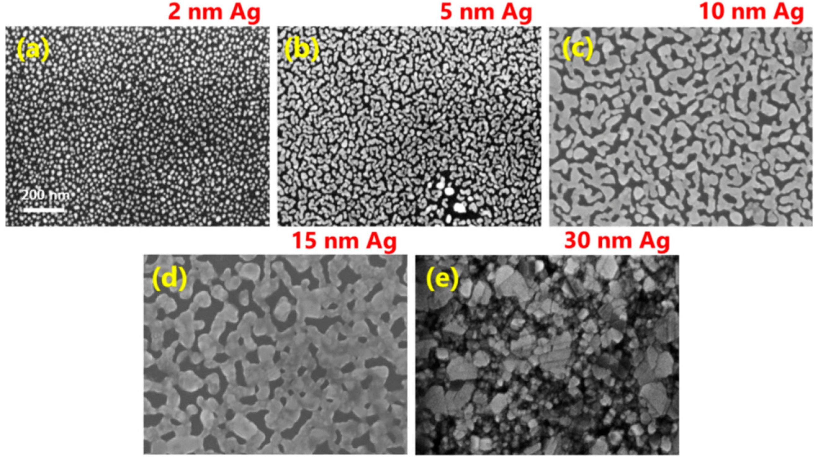
- Shtepliuk, I.; Ivanov, I.G.; Pliatsikas, N.; Ben Sedrine, N.; Andersson, O.; Iakimov, T.; Jamnig, A.; Sarakinos, K.; Yakimova, R. Interplay between thin silver films and epitaxial graphene. Surf. Coat. Technol. 2020, 381, 125200. [Google Scholar] [CrossRef]
- Shtepliuk, I.; Ivanov, I.G.; Pliatsikas, N.; Iakimov, T.; Jamnig, A.; Sarakinos, K.; Yakimova, R. Probing the uniformity of silver-doped epitaxial graphene by micro-Raman mapping. Phys. B 2020, 580, 411751. [Google Scholar] [CrossRef]
- Shtepliuk, I.; Ivanov, I.G.; Pliatsikas, N.; Iakimov, T.; Beshkova, M.; Sarakinos, K.; Yakimova, R. Exploring the Interface Landscape of Noble Metals on Epitaxial Graphene. Phys. Status Solidi A 2021, 2000673. [Google Scholar] [CrossRef]
- Shtepliuk, I.; Vagin, M.; Ivanov, I.G.; Iakimov, T.; Reza Yazdi, G.; Yakimova, R. Lead (Pb) interfacing with epitaxial graphene. Phys. Chem. Chem. Phys. 2018, 20, 17105–17116. [Google Scholar] [CrossRef] [Green Version]
- Shtepliuk, I.; Vagin, M.; Yakimova, R. Insights into the Electrochemical Behavior of Mercury on Graphene/SiC Electrodes. C—J. Carbon Res. 2019, 5, 51. [Google Scholar] [CrossRef] [Green Version]
- Shtepliuk, I.; Vagin, M.; Yakimova, R. Electrochemical Deposition of Copper on Epitaxial Graphene. Appl. Sci. 2020, 10, 1405. [Google Scholar] [CrossRef] [Green Version]
- Zheng, J.; Zhao, Q.; Tang, T.; Yin, J.; Quilty, C.D.; Renderos, G.D.; Liu, X.; Deng, Y.; Wang, L.; Bock, D.C.; et al. Reversible epitaxial electrodeposition of metals in battery anodes. Science 2019, 366, 645–648. [Google Scholar] [CrossRef] [PubMed]
- Shtepliuk, I.; Ivanov, I.G.; Vagin, M.; Khan, Z.; Iakimov, T.; Pliatsikas, N.; Sarakinos, K.; Giannazzo, F.; Yakimova, R. Manipulation of epitaxial graphene towards novel properties and applications. Mater. Today Proc. 2020, 20, 37–45. [Google Scholar] [CrossRef]
- Lin, Y.-M.; Dimitrakopoulos, C.; Jenkins, K.A.; Farmer, D.B.; Chiu, H.-Y.; Grill, A.; Avouris, P. 100-GHz transistors from wafer-scale epitaxial graphene. Science 2010, 327, 662. [Google Scholar] [CrossRef] [Green Version]
- Fisichella, G.; Schilirò, E.; Di Franco, S.; Fiorenza, P.; Lo Nigro, R.; Roccaforte, F.; Ravesi, S.; Giannazzo, F. Interface electrical properties of Al2O3 thin films on graphene obtained by atomic layer deposition with an in situ seedlike layer. ACS Appl. Mater. Interfaces 2017, 9, 7761–7771. [Google Scholar] [CrossRef]
- Giannazzo, F.; Greco, G.; Schilirò, E.; Lo Nigro, R.; Deretzis, I.; La Magna, A.; Roccaforte, F.; Iucolano, F.; Ravesi, S.; Frayssinet, E.; et al. High-performance graphene/AlGaN/GaN Schottky junctions for hot electron transistors. ACS Appl. Electron. Mater. 2019, 1, 2342–2354. [Google Scholar] [CrossRef]
- Sagade, A.A.; Neumaier, D.; Schall, D.; Otto, M.; Pesquera, A.; Centeno, A.; Elorza, A.Z.; Kurz, H. Highly air stable passivation of graphene based field effect devices. Nanoscale 2015, 7, 3558–3564. [Google Scholar] [CrossRef] [PubMed]
- Schilirò, E.; Lo Nigro, R.; Panasci, S.E.; Gelardi, F.M.; Agnello, S.; Yakimova, R.; Roccaforte, F.; Giannazzo, F. Aluminum oxide nucleation in the early stages of atomic layer deposition on epitaxial graphene. Carbon 2020, 169, 172–181. [Google Scholar] [CrossRef]
- Giannazzo, F.; Schilirò, E.; Lo Nigro, R.; Roccaforte, F.; Yakimova, R. Atomic Layer Deposition of High-k Insulators on Epitaxial Graphene: A Review. Appl. Sci. 2020, 10, 2440. [Google Scholar] [CrossRef] [Green Version]


Publisher’s Note: MDPI stays neutral with regard to jurisdictional claims in published maps and institutional affiliations. |
© 2021 by the authors. Licensee MDPI, Basel, Switzerland. This article is an open access article distributed under the terms and conditions of the Creative Commons Attribution (CC BY) license (https://creativecommons.org/licenses/by/4.0/).
Share and Cite
Shtepliuk, I.; Giannazzo, F.; Yakimova, R. Epitaxial Graphene on 4H-SiC (0001) as a Versatile Platform for Materials Growth: Mini-Review. Appl. Sci. 2021, 11, 5784. https://doi.org/10.3390/app11135784
Shtepliuk I, Giannazzo F, Yakimova R. Epitaxial Graphene on 4H-SiC (0001) as a Versatile Platform for Materials Growth: Mini-Review. Applied Sciences. 2021; 11(13):5784. https://doi.org/10.3390/app11135784
Chicago/Turabian StyleShtepliuk, Ivan, Filippo Giannazzo, and Rositsa Yakimova. 2021. "Epitaxial Graphene on 4H-SiC (0001) as a Versatile Platform for Materials Growth: Mini-Review" Applied Sciences 11, no. 13: 5784. https://doi.org/10.3390/app11135784
APA StyleShtepliuk, I., Giannazzo, F., & Yakimova, R. (2021). Epitaxial Graphene on 4H-SiC (0001) as a Versatile Platform for Materials Growth: Mini-Review. Applied Sciences, 11(13), 5784. https://doi.org/10.3390/app11135784