Article

Influence of Hydrogen Ions on the Performance of Thin-Film Transistors with Solution-Processed AlOx Gate Dielectrics

State Key Laboratory of Luminescent Materials and Devices, South China University of Technology, Guangzhou 510640, China
*
Author to whom correspondence should be addressed.
Appl. Sci. 2021, 11(10), 4393; https://doi.org/10.3390/app11104393
Submission received: 19 March 2021 / Revised: 4 May 2021 / Accepted: 7 May 2021 / Published: 12 May 2021
(This article belongs to the Section Materials Science and Engineering)

Abstract

:
Over the past decade, there have been many reports on solution-processed oxide thin-film transistors (TFTs) with high mobility (even >100 cm2 V−1s−1). However, the capacitance uncertainty of the solution-processed oxide gate dielectrics leads to serious overestimation of the mobility. Here, solution-processed AlOx dielectrics are investigated systematically, and the effect of mobile ions on the frequency-dependent capacitance of the solution-processed AlOx dielectrics is also studied. It was found that the capacitance of the AlOx depends on the frequency seriously when the annealing temperature is lower than 300 °C, and the water treatment causes more seriously frequency-dependent capacitance. The strong frequency-dependent capacitance of the AlOx annealed at 250 or 300 °C is attributed to relaxation polarization of the weakly bound ions in the incompletely decomposed AlOx films. The water treatment introduces a large number of protons (H+) that would migrate to the ITO/AlOx interface under a certain electric field and form an electric double layer (EDL) that has ultrahigh capacitance at low frequency.

1. Introduction

In the past decade, oxide thin-film transistors (TFTs) have drawn much attention for their potential applications in large-size, high-frequency, transparent, flexible, or energy-saving displays due to the advantages of ultralow off-current, relatively high field-effect mobility, good uniformity in large size, etc. [1,2]. In oxide TFTs, the gate dielectric layer plays an important role; therefore, it is necessary to investigate the influence the of gate dielectric materials and their fabrication process on the performance of the oxide TFTs. A number of gate dielectrics such as HfO2 [3,4], Al2O3 [5,6,7,8,9,10], and ZrO2 [11,12,13,14,15], and giant dielectric constant materials [16] have been investigated for oxide TFTs. However, the effect of the water-induced mobile ions of the gate dielectrics on the TFT performance has not been studied in detailed yet.
Compared to the traditional vacuum-processed method, the solution-processed method is more attractive for the advantages of low-cost, high-throughput, and easy chemical composition control [17]. Recently, solution-processed AlOx gate dielectric has drawn attention due to the high dielectric constant, low leakage current, and good compatibility with oxide semiconductors [7,18,19]. However, the capacitance of solution-processed AlOx dielectrics depends on the preparing processes strongly [20,21]. Therefore, it is necessary to investigate the mobile ions and residue groups in the solution-processed AlOx dielectrics to improve the insulating properties. In addition, there have been many reports on solution-processed oxide TFTs with high field-effect mobility (even >100 cm2 V−1s−1). These values are highly controversial, because the capacitance used to calculate the field-effect mobility is 1kHz or above, which is much lower than the actual capacitance during TFT measuring (the gate sweeps at a certain VGS step, which means that the charging of the gate dielectric is step-by-step, meaning quasistatic capacitance is more appropriate for the mobility calculation). For this reason, it is indispensable to regulate the capacitance measurement for calculating the field-effect mobility of TFTs. In this paper, the properties of solution-processed AlOx dielectrics are investigated systematically, and the effect of mobile protons on the frequency-dependent capacitance and on the performance of the oxide TFTs is also studied.

2. Experiment

The AlOx precursor solution was prepared by dissolving 0.2 M Al(NO3)3·9H2O in 2-methoxyethanol, stirred at room temperature for 24 h, and aged for 6 h. The precursor materials, including solutes and solvents, were purchased from Aladdin. The AlOx precursor films were deposited by spin-coating at 3000 rpm for 30 s and then soft-baked on a hot plate at 150 °C for 10 min to remove the solvents. After that, the AlOx precursor films were annealed in the air at different temperature of 250, 300, and 350 °C for 1 h. Each sample was baked at 150 °C for 10 min immediately after spin-coating. Then, each sample was annealed separately at different temperature for 1 h. The thickness of AlOx is about 57 ± 3 nm.
TFTs with AlOx gate dielectric layer and InScOx (In2O3:Sc2O3 = 98:2 wt%) semiconductor layer were constructed with a bottom-gate top-contact structure. A 200 nm indium tin oxide (ITO, In:Sn = 9:1) gate electrode was deposited onto the glass substrate by DC magnetron sputtering (70 W) under argon pressure of 0.5 Pa at room temperature through a shading mask. Then, a layer of AlOx dielectric film was deposited onto the ITO gate electrode using the process described above. After that, the InScOx semiconductor layer (20 nm) was deposited by RF magnetron sputtering (60 W) under argon pressure of 0.5 Pa at room temperature through a shading mask. The ITO source and drain electrodes (200 nm) were deposited onto the InScOx semiconductor layer by DC magnetron sputtering with the same conditions as that of the gate deposition. The channel width (W) and length (L) were defined by a shading mask to be 800 and 200 μm, respectively. Finally, the TFT devices were post-annealed at 250 °C for 1 h. The ITO/AlOx/ITO metal-insulator-metal (MIM) devices were prepared by depositing a circular ITO top electrode (200 nm) with a diameter of 0.04 mm onto the AlOx film by DC magnetron sputtering.
To investigate the effect of hydrogen ions (H+) on the dielectric properties of the AlOx layer, water treatment was performed on the surface of the ITO gate electrode before spin-coating the AlOx film. Because the solution-processed AlOx film is very sensitive to moisture, water treatment is a simple way to increase the density of the mobile H+. The water treatment process was performed by spin-coating deionized water at a speed of 3000 rpm for 30 s onto the surface of the ITO gate electrode to introduce large amount of adsorbed H+ and OH groups at the ITO/AlOx interface. The ITO surface is treated by O2 plasma before water treatment. The contact angles of the plasma treated and plasma + water treated ITO surfaces are 5.03° and 3.93°, respectively.
The thermal behavior of AlOx precursor was analyzed by thermogravimetric analyses (TG). The chemical composition, water adsorption, and proton quantity behavior of the AlOx films were characterized by X-ray photoelectron spectroscopy (XPS, Thermo Fisher Scientific Inc, ESCALAB250Xi), infrared spectroscopy (FT-IR), and time-of-flight secondary-ion mass spectrometry (TOF-SIMS), respectively. The electrical properties of MIM and TFTs were characterized by semiconductor parameter analyzer (Keysight B1500A).

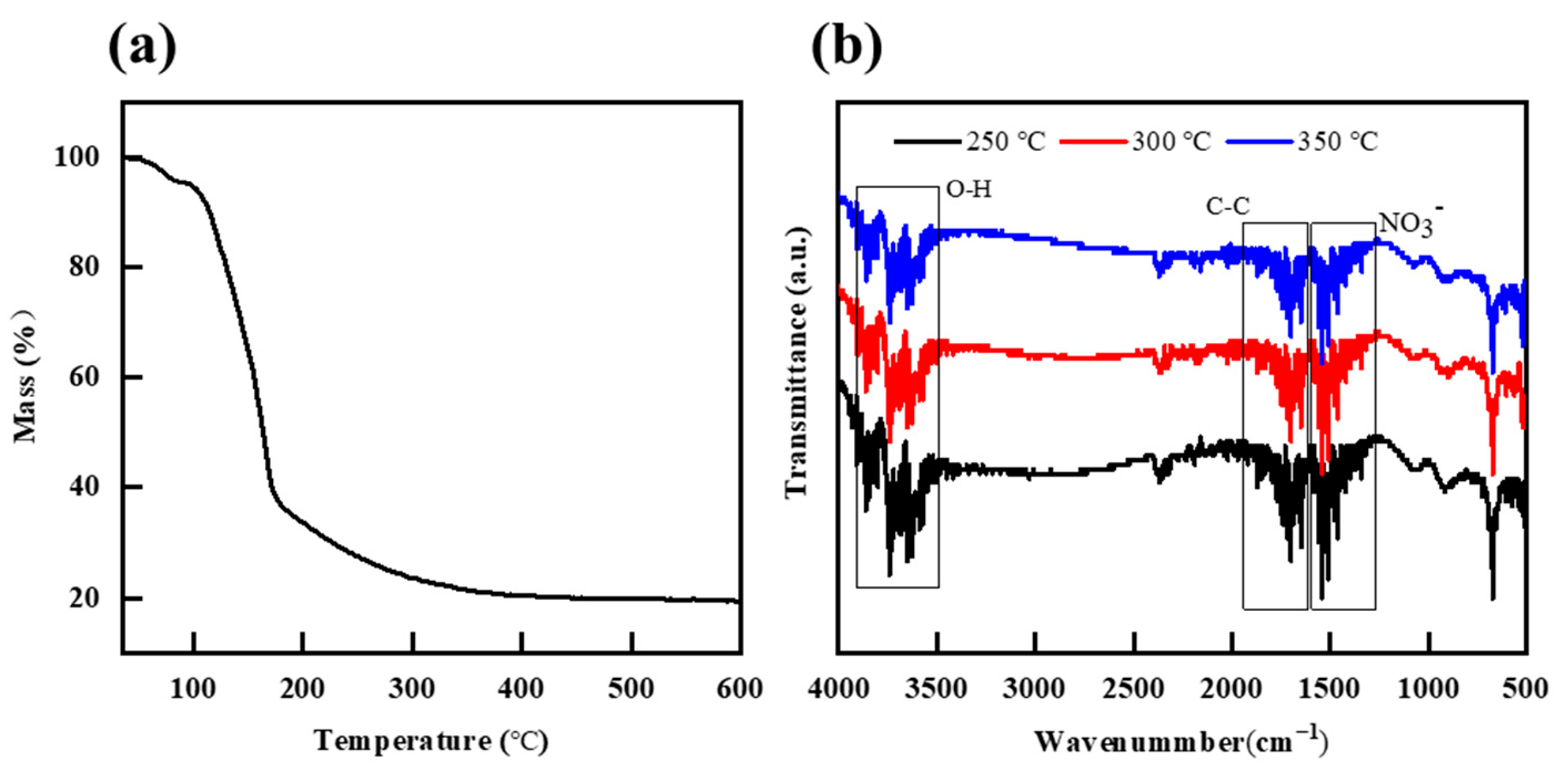
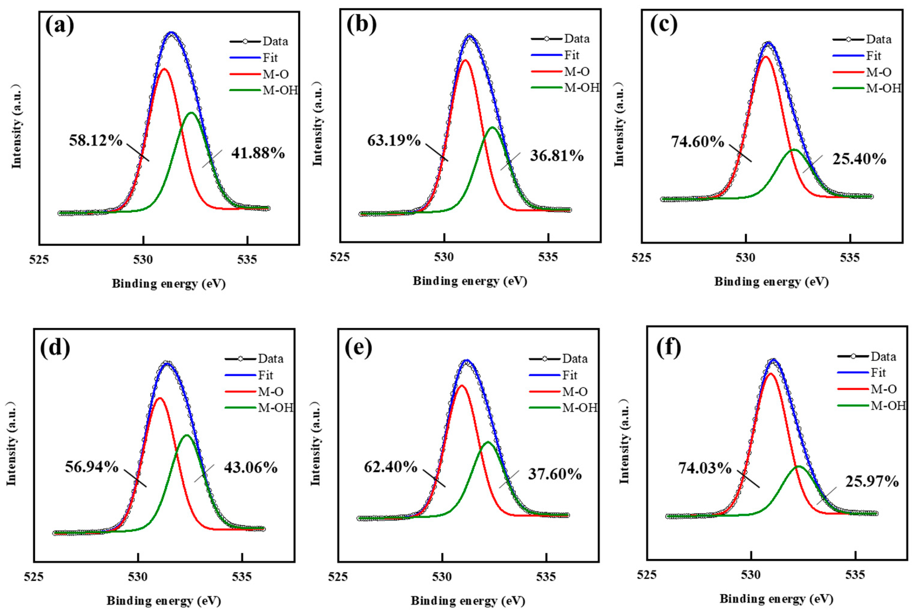
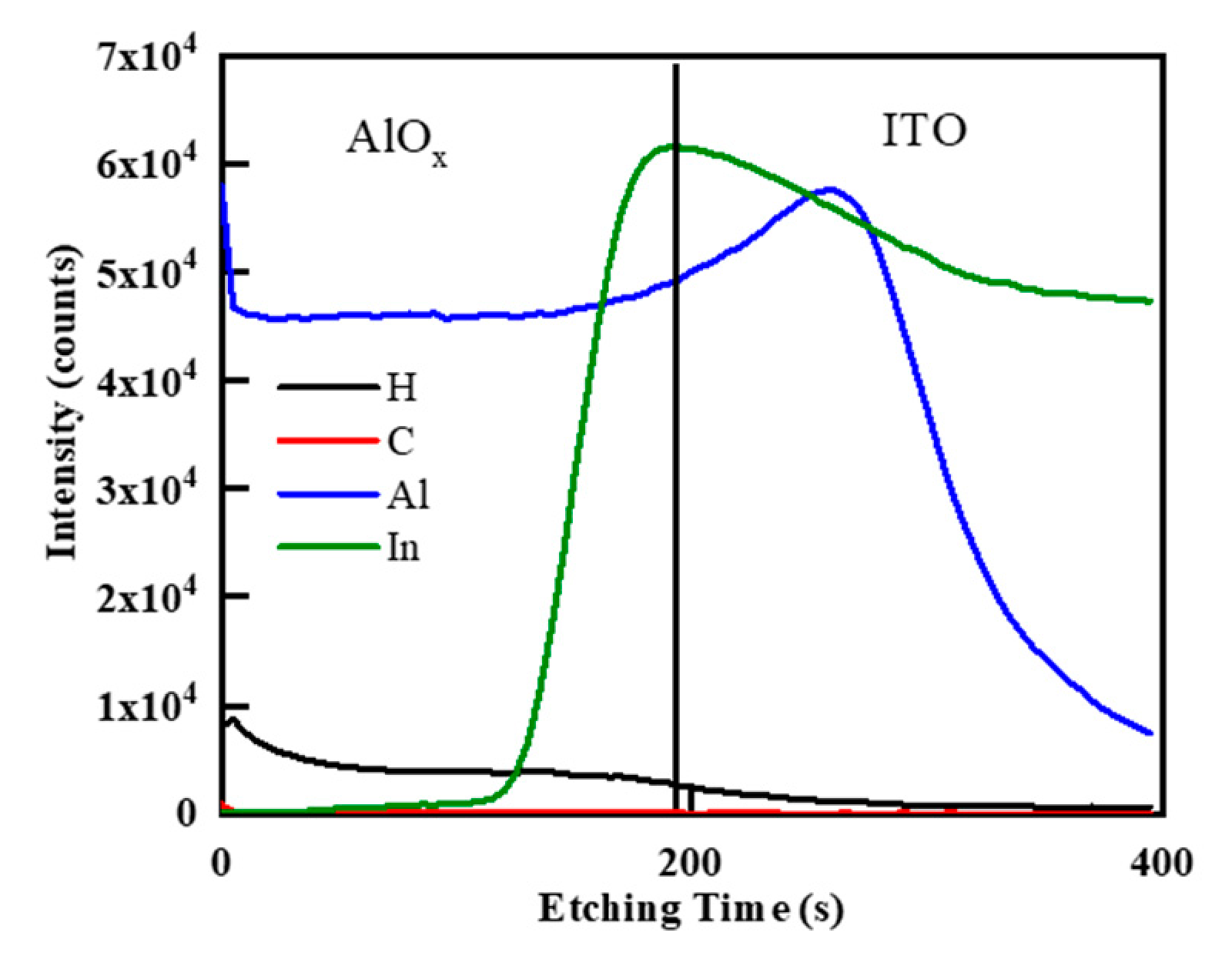
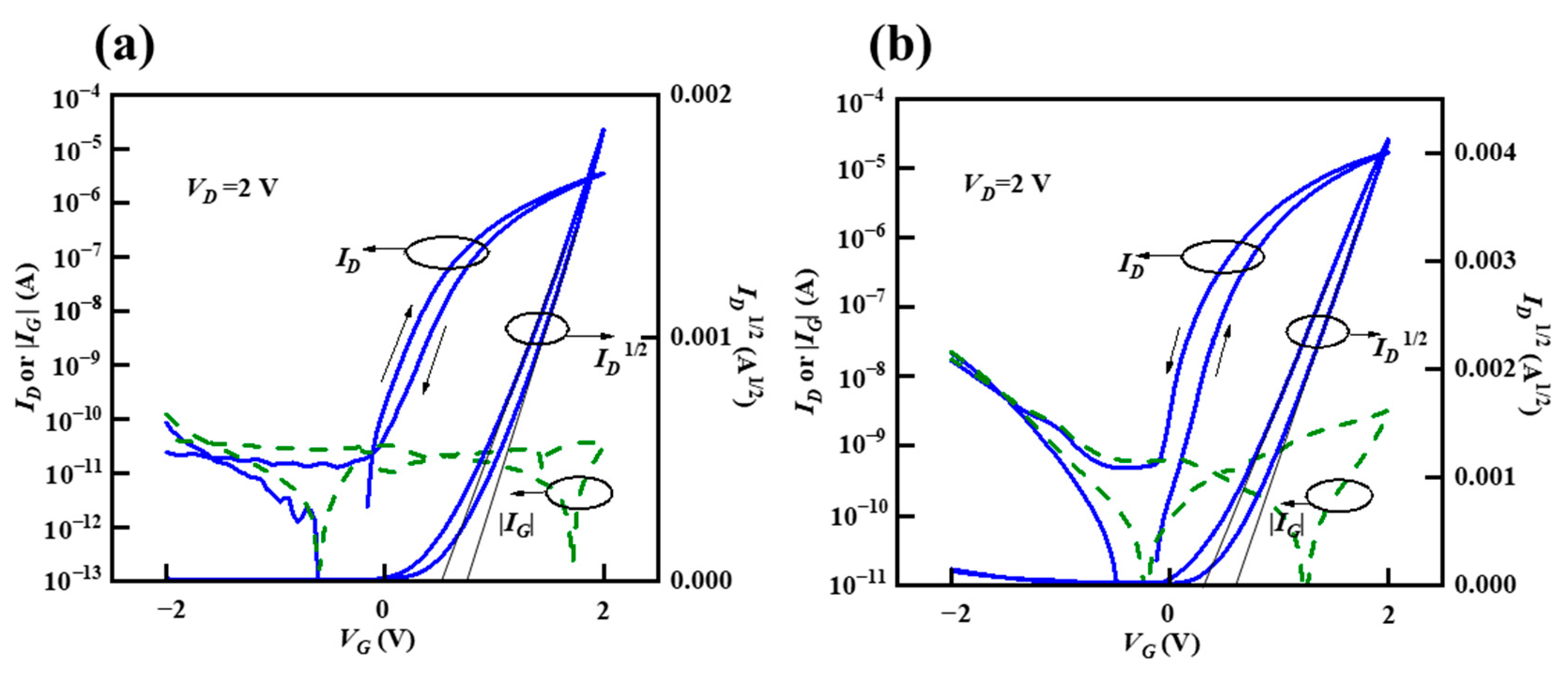
3. Results and Discussion

Figure 1a shows the TG curve of AlOx precursor. It reveals an initial mass loss event of ~60%, occurring around 120–180 °C, which is assigned to the removal of solvent and organic residues and the dehydroxylation of AlOx precursor. Then, a slow mass loss is observed around 180–350 °C, with weight stabilizing at close to 20% by 350 °C, indicating complete conversion of precursors to form the dense metal oxide. Figure 1b shows the FT-IR spectra of AlOx films annealed at different temperatures. The peaks around 1700 cm−1 (C=C stretching) and 1500 cm−1 (N-O asymmetric stretching) are attributed to the residual organic elements and the undecomposed precursor metal salts, respectively [22,23]. As the annealing temperature increases from 250 to 350 °C, the intensity of the peaks decreases continuously, which is consistent with the TG analysis. The peaks in the range of 3500–3800 cm−1 is due to the peaks of O-H stretching plausibly resulting from surface hydroxylation [22,23].
Figure 2 shows the XPS O 1s peaks of the AlOx films with different annealing temperature. Each O 1s spectrum was fitted by two Gaussian distributions with binding energies at 531 and 532.3 eV, corresponding to the contribution of lattice oxygen (M–O–M), and hydroxyl group (M–OH), respectively [7,10,18,21,22]. The relative concentrations of M–OH related oxygen for the untreated samples annealed at 250, 300, and 350 °C are 41.88%, 36.81%, and 25.40%, respectively, while the water-treated samples annealed at 250, 300, and 350 °C exhibit higher M–OH concentrations of 43.06%, 37.60 %, and 25.97%, respectively. The result is in accordance with the change of O-H stretching peaks in the FT-IR spectra (Figure 1b). It indicates that there are plenty of hydroxyl groups on the surface of AlOx film annealed at 250 °C, and the number of them can be reduced effectively when the annealing temperature reaches 350 °C. The concentration difference between the water-treated and untreated samples narrows as the annealing temperature increases, because the water molecules are easier to be dislodged at higher annealing temperature.
The insulating properties of AlOx films were evaluated with a MIM structure of ITO/AlOx/ITO. Figure 3a shows the frequency dependence of capacitance of the MIM devices. Interestingly, the capacitance decreases as the annealing temperature increases at lower frequency regime (<10 kHz), while it increases as the annealing temperature increases at higher frequency regime (>1 MHz). In addition, the capacitance of the MIM devices annealed at 250 or 300 °C depends on the frequency greatly, while the AlOx film annealed at 350 °C is almost independent of the measuring frequency (when the measuring frequency is lower than 100 kHz). The areal capacitances at 1 kHz for the MIM devices annealed at 250, 300, and 350 °C are 179.1, 166.3, and 148.1 nF/cm2, respectively; and the areal quasistatic (QS) capacitances (see Figure 3b) for the devices annealed at 250, 300, and 350 °C are 288.9, 263.4, and 152.8 nF/cm2, respectively. It shows that the areal quasistatic capacitance of the MIM devices annealed at 250 or 300 °C is much higher than those measured at 1 kHz, while there is no much difference between the areal quasistatic capacitance and the areal capacitance at 1 kHz for the one annealed at 350 °C. The strong frequency-dependent capacitance of the MIM devices annealed at 250 or 300 °C is attributed to relaxation polarization of the weakly bound ions in the incompletely decomposed AlOx films. Especially, the protons (H+), which can move in the whole AlOx film, move to the ITO/AlOx interface and form an electric double layer (EDL) that has ultrahigh capacitance at very low frequency [24,25].
To further investigate the effect of mobile hydrogen-related ions on the low-frequency capacitance of the AlOx films, the surface of the bottom electrode (ITO) was treated by water before spin-coating the AlOx precursor on it. The water treatment can introduce large amounts of the adsorbed water molecules at the ITO/AlOx interface that would further form hydrogen and OH groups. Figure 3c shows the frequency dependence of capacitance of the MIM devices with water treatment. It can be seen that the capacitance of all devices (even annealed at 350 °C) depends on the frequency seriously. The areal capacitances at 1 kHz of the MIM devices annealed at 250, 300, and 350 °C are 387.9, 295.3, and 268.9 nF/cm2, respectively. However, the areal quasi-static capacitances of the MIM devices annealed at 250, 300, and 350 °C are as high as 1520, 846, and 647 nF/cm2 (see Figure 3d). The extremely high quasistatic capacitance is most probably attributed to H+ ions which are small and easy to be driven by the electric field. The H+ ions in oxide films are generally associated with oxygen atoms to form a three-coordinate oxygen center (M–OH+–M), and the motion of H+ ions is relied on “a sequence of hops” from one bridging oxygen atom to another [13,24,26]. When a voltage is applied to the MIM device, the H+ ions migrate to the AlOx/ITO interface by a sequence of hops and form a very thin EDL with an extremely large capacitance. Under an electric field of 0.3 MV/cm (2 V), the leakage current density (J) of the MIM devices without water treatment annealed at 250, 300, and 350 ℃ are 3.2 × 10⁸, 2.4 × 10⁻⁸, and 1.4 × 10⁻⁸ A/cm2, respectively, corresponding to much higher J of 5.5 × 10⁻⁷, 4.5 × 10⁻⁷, and 2.6 × 10⁻⁷ A/cm2 for the water-treated ones (not shown). The breakdown field of the MIM devices without water treatment annealed at 250, 300, and 350 ℃ are 1.9, 2.9, and 3.2 MV/cm, respectively (not shown). Interestingly, the leakage current for the water-treated MIM devices increases greatly at ~0.3 MV, but there are not apparent breakdown points. The difference may be attributed to the large amount of movable H+ ions in the water-treated AlOx samples, which form leakage current paths. To verify the existence of H+ ions in the AlOx films, TOF-SIMS experiments were carried out. Figure 4 shows the depth-profile element distribution of the water-treated AlOx/ITO sample annealed at 350 °C. The intensities for the carbon signal are very weak, revealing little carbon-related residuals. By contrast, there are a number of hydrogens in the whole AlOx dielectric. It is worth noting that the hydrogen distribution is not uniform with the density gradually decreasing from AlOx surface to the AlOx/ITO interface. The results confirm that a large amount of hydrogen elements is introduced during treatment. The obvious overlap of Al and In signals is mainly due to the diffusion of Al and In elements at the ITO/AlOx interface.
Finally, TFTs with AlOx gate insulator and InScOx channel layer were fabricated to verify the formation of EDL. InScOx semiconductor can effectively decrease the influence of water and oxygen in the environment on the stability of TFTs [27]. Figure 5a,b shows the transfer curves of the TFTs without and with water treatment, respectively. Interestingly, the TFT without water treatment exhibits clockwise hysteresis in the transfer curve between forward and reverse gate sweeps, while the one with water treatment exhibits anticlockwise hysteresis. The anticlockwise hysteresis of the water-treated TFT is ascribed to the low migration speed of the H+ ions [28]. When the gate voltage increases, the H+ ions migrate to the AlOx/InScOx interface slowly; after the gate voltage reaches the highest value and begin to decrease, some of the H+ ions still move toward the AlOx/InScOx interface, causing further increase in the EDL capacitance. As a result, the current for the reverse sweep is higher than that for the forward sweep (due to the higher capacitance). The saturation mobility (μsat) was extracted by fitting a straight line to the plot of the square root of the ID versus VG and using the following equation:
I D = W μ s a t C 2 L V G V t h 2
where C is the areal capacitance of the gate dielectric, and W and L are the channel width and length, respectively. The calculated mobilities for forward- and reversed-sweep curves of the TFTs without water treatment is 6.75 and 9.71 cm2 V−1s−1, respectively, while those for forward- and reversed-sweep curves of water-treated ones are 6.72 and 5.02 cm2 V−1s−1, respectively. Although the TFT with water treatment is high on-current, the mobility is lower than that of the TFT without water treatment. The results confirm that the mobility of the water-treated TFTs is overestimated if using the same capacitance (Ci) of the untreated TFTs for calculating mobility. The key properties of the TFTs with/without water treatment are summarized in Table 1.

4. Conclusions

In summary, MIM and TFT devices based on solution-processed AlOx dielectrics were fabricated, and the effect of mobile ions on the frequency-dependent capacitance of the solution-processed AlOx dielectrics is studied. It is found that the capacitance of the AlOx dielectrics annealed at 250 or 300 °C depends on the frequency greatly, while the AlOx film annealed at 350 °C is almost independent of the frequency (<100 kHz); and the water treatment causes more seriously frequency-dependent capacitance. The strong frequency-dependent capacitance of the AlOx annealed at 250 or 300 °C is attributed to relaxation polarization of the weakly bound ions in the incompletely decomposed AlOx films. The water treatment introduces a large number of protons (H+) that would migrate to the ITO/AlOx interface under a certain electric field and form an electric double layer (EDL) that has ultrahigh capacitance at low frequency. The oxide TFTs based on water treated AlOx dielectrics exhibit anticlockwise hysteresis in the transfer curves that confirm existence of mobile ions in the AlOx films. The calculated mobilities for forward- and reversed-sweep curves of the TFTs without water treatment is 6.75 and 9.71 cm2 V−1s−1, respectively, while those for forward- and reversed-sweep curves of water-treated ones are 6.72 and 5.02 cm2 V−1s−1, respectively. Although the TFT with water treatment is high on-current, the mobility is lower than that of the TFT without water treatment. The results confirm that the mobility of the water-treated TFTs is overestimated if using the same capacitance (Ci) of the untreated TFTs for calculating mobility.

Author Contributions

Conceptualization, L.L., Y.W. and P.H.; formal analysis, Y.W. and Y.L.; investigation, C.D., S.C. and J.P.; writing—original draft, Y.W.; writing—review editing, L.L. All authors have read and agreed to the published version of the manuscript.

Funding

This research was funded by the National Natural Science Foundation of China (Grant Nos. 62022034, 51673068, 62074059), the Guangdong Natural Science Foundation (Grant No. 2017A030306007), the Guangdong Project of R&D Plan in Key Areas (Grant Nos. 2020B010180001, and 2019B010934001), the Guangdong Major Project of Basic and Applied Basic Research (No. 2019B030302007), and the Key Project of Guangzhou Science and Technology Plan (Grant No. 201904020034).

Institutional Review Board Statement

Not applicable.

Informed Consent Statement

Not applicable.

Data Availability Statement

Not applicable.

Acknowledgments

Authors would like to extend thanks to Zhuo Chen for his support in capacitance test and data analysis.

Conflicts of Interest

The authors declare no conflict of interest.

References

  1. Fortunato, E.; Barquinha, P.; Martins, R. Oxide semiconductor thin-film transistors: A review of recent advances. Adv. Mater. 2012, 24, 2945–2986. [Google Scholar] [CrossRef]
  2. Nomura, K.; Ohta, H.; Takagi, A.; Kamiya, T.; Hirano, M.; Hosono, H. Room-temperature fabrication of transparent flexible thin-film transistors using amorphous oxide semiconductors. Nature 2004, 432, 488–492. [Google Scholar] [CrossRef]
  3. Cai, W.; Brownless, J.; Zhang, J.; Li, H.; Tillotson, E.; Hopkinson, D.G.; Haigh, S.J.; Song, A. Solution-Processed HfOx for Half-Volt Operation of InGaZnO Thin-Film Transistors. ACS Appl. Electron. Mater. 2019, 1, 1581–1589. [Google Scholar] [CrossRef]
  4. Jiang, K.; Anderson, J.T.; Hoshino, K.; Li, D.; Wager, J.F.; Keszler, D.A. Low-Energy Path to Dense HfO2Thin Films with Aqueous Precursor. Chem. Mater. 2011, 23, 945–952. [Google Scholar] [CrossRef]
  5. Daunis, T.B.; Tran, J.M.H.; Hsu, J.W.P. Effects of Environmental Water Absorption by Solution-Deposited Al2O3 Gate Dielectrics on Thin Film Transistor Performance and Mobility. ACS Appl. Mater. Interfaces 2018, 10, 39435–39440. [Google Scholar] [CrossRef]
  6. Carlos, E.; Dellis, S.; Kalfagiannis, N.; Koutsokeras, L.; Koutsogeorgis, D.C.; Branquinho, R.; Martins, R.; Fortunato, E. Laser induced ultrafast combustion synthesis of solution-based AlOx for thin film transistors. J. Mater. Chem. C 2020, 8, 6176–6184. [Google Scholar] [CrossRef]
  7. Nayak, P.K.; Hedhili, M.N.; Cha, D.; Alshareef, H.N. High performance In2O3 thin film transistors using chemically derived aluminum oxide dielectric. Appl. Phys. Lett. 2013, 103. [Google Scholar] [CrossRef] [Green Version]
  8. Park, J.H.; Kim, K.; Yoo, Y.B.; Park, S.Y.; Lim, K.-H.; Lee, K.H.; Baik, H.K.; Kim, Y.S. Water adsorption effects of nitrate ion coordinated Al2O3 dielectric for high performance metal-oxide thin-film transistor. J. Mater. Chem. C 2013, 1. [Google Scholar] [CrossRef]
  9. Park, K.; Jeon, G.; Lee, S.; Ko, J.; Park, S.-H. Effects of Hydroxyl Group in AlO x Gate Insulator on the Negative Bias Illumination Instability of In-Ga-Zn-O Thin Film Transistors. Phys. Status Solidi (a) 2019, 216, 1800737. [Google Scholar] [CrossRef]
  10. Xia, W.; Xia, G.; Tu, G.; Dong, X.; Wang, S.; Liu, R. Sol-gel processed high-k aluminum oxide dielectric films for fully solution-processed low-voltage thin-film transistors. Ceram. Int. 2018, 44, 9125–9131. [Google Scholar] [CrossRef]
  11. Park, J.H.; Yoo, Y.B.; Lee, K.H.; Jang, W.S.; Oh, J.Y.; Chae, S.S.; Baik, H.K. Low-temperature, high-performance solution-processed thin-film transistors with peroxo-zirconium oxide dielectric. ACS Appl. Mater. Interfaces 2013, 5, 410–417. [Google Scholar] [CrossRef]
  12. Zhu, C.; Liu, A.; Liu, G.; Jiang, G.; Meng, Y.; Fortunato, E.; Martins, R.; Shan, F. Low-temperature, nontoxic water-induced high-k zirconium oxide dielectrics for low-voltage, high-performance oxide thin-film transistors. J. Mater. Chem. C 2016, 4, 10715–10721. [Google Scholar] [CrossRef]
  13. Li, Y.; Lan, L.; Hu, S.; Gao, P.; Dai, X.; He, P.; Li, X.; Peng, J. Fully Printed Top-Gate Metal–Oxide Thin-Film Transistors Based on Scandium-Zirconium-Oxide Dielectric. IEEE Trans. Electron. Devices 2019, 66, 445–450. [Google Scholar] [CrossRef]
  14. Lee, C.-G.; Dodabalapur, A. Solution-Processed High-k Dielectric, ZrO2, and Integration in Thin-Film Transistors. J. Electron. Mater. 2012, 41, 895–898. [Google Scholar] [CrossRef]
  15. Xu, W.; Wang, H.; Ye, L.; Xu, J. The role of solution-processed high-κ gate dielectrics in electrical performance of oxide thin-film transistors. J. Mater. Chem. C 2014, 2. [Google Scholar] [CrossRef]
  16. Chen, Z.; Lan, L.; Peng, J. Approaching subthreshold-swing limit for thin-film transistors by using a giant-dielectric-constant gate dielectric. RSC Adv. 2019, 9, 27117–27124. [Google Scholar] [CrossRef] [Green Version]
  17. Chen, R.; Lan, L. Solution-processed metal-oxide thin-film transistors: A review of recent developments. Nanotechnology 2019, 30, 312001. [Google Scholar] [CrossRef]
  18. Xu, W.; Wang, H.; Xie, F.; Chen, J.; Cao, H.; Xu, J.B. Facile and environmentally friendly solution-processed aluminum oxide dielectric for low-temperature, high-performance oxide thin-film transistors. ACS Appl. Mater. Interfaces 2015, 7, 5803–5810. [Google Scholar] [CrossRef]
  19. Daunis, T.B.; Barrera, D.; Gutierrez-Heredia, G.; Rodriguez-Lopez, O.; Wang, J.; Voit, W.E.; Hsu, J.W.P. Solution-processed oxide thin film transistors on shape memory polymer enabled by photochemical self-patterning. J. Mater. Res. 2018, 33, 2454–2462. [Google Scholar] [CrossRef]
  20. Park, H.; Nam, Y.; Jin, J.; Bae, B.-S. Space charge-induced unusually-high mobility of a solution-processed indium oxide thin film transistor with an ethylene glycol incorporated aluminum oxide gate dielectric. RSC Adv. 2015, 5, 102362–102366. [Google Scholar] [CrossRef]
  21. Jo, J.W.; Kim, J.; Kim, K.T.; Kang, J.G.; Kim, M.G.; Kim, K.H.; Ko, H.; Kim, J.; Kim, Y.H.; Park, S.K. Highly stable and imperceptible electronics utilizing photoactivated heterogeneous sol-gel metal-oxide dielectrics and semiconductors. Adv. Mater. 2015, 27, 1182–1188. [Google Scholar] [CrossRef] [PubMed]
  22. Xu, W.; Long, M.; Zhang, T.; Liang, L.; Cao, H.; Zhu, D.; Xu, J.-B. Fully solution-processed metal oxide thin-film transistors via a low-temperature aqueous route. Ceram. Int. 2017, 43, 6130–6137. [Google Scholar] [CrossRef]
  23. Kim, H.; Maeng, S.; Lee, S.; Kim, J. Improved Performance and Operational Stability of Solution-Processed InGaSnO (IGTO) Thin Film Transistors by the Formation of Sn–O Complexes. ACS Appl. Electron. Mater. 2021, 3, 1199–1210. [Google Scholar] [CrossRef]
  24. Jiang, J.; Wan, Q.; Sun, J.; Lu, A. Ultralow-voltage transparent electric-double-layer thin-film transistors processed at room-temperature. Appl. Phys. Lett. 2009, 95, 152114. [Google Scholar] [CrossRef]
  25. Mottram, A.D.; Pattanasattayavong, P.; Isakov, I.; Wyatt-Moon, G.; Faber, H.; Lin, Y.-H.; Anthopoulos, T.D. Electron mobility enhancement in solution-processed low-voltage In2O3 transistors via channel interface planarization. AIP Adv. 2018, 8, 065015. [Google Scholar] [CrossRef]
  26. Norby, T.; Widerøe, M.; Glöckner, R.; Larring, Y. Hydrogen in oxides. Dalton Trans. 2004, 3012–3018. [Google Scholar] [CrossRef]
  27. Song, W.; Lan, L.; Xiao, P.; Lin, Z.; Sun, S.; Li, Y.; Song, E.; Gao, P.; Zhang, P.; Wu, W.; et al. High-Mobility and Good-Stability Thin-Film Transistors With Scandium-Substituted Indium Oxide Semiconductors. IEEE Trans. Electron. Devices 2016, 63, 4315–4319. [Google Scholar] [CrossRef]
  28. Banger, K.; Warwick, C.; Lang, J.; Broch, K.; Halpert, J.E.; Socratous, J.; Brown, A.; Leedham, T.; Sirringhaus, H. Identification of dipole disorder in low temperature solution processed oxides: Its utility and suppression for transparent high performance solution-processed hybrid electronics. Chem. Sci. 2016, 7, 6337–6346. [Google Scholar] [CrossRef] [Green Version]
Figure 1. (a) TG curve of the AlOx precursor from 35 to 600 °C. (b) FT-IR spectra of the AlOx films annealed at different temperatures.
Applsci 11 04393 g001
Figure 2. XPS O1s spectra of the untreated AlOx films annealed at (a) 250, (b) 300, and (c) 350 °C; and XPS O1s spectra of the water treated AlOx films annealed at (d) 250, (e) 300, and (f) 350 °C.
Applsci 11 04393 g002
Figure 3. (a) Capacitance-frequency curves and (b) quasistatic capacitance-voltage curves of the AlOx dielectrics without water treatment; (c) Capacitance-frequency curves; and (d) quasistatic capacitance-voltage curves of the AlOx dielectrics with water treatment.
Applsci 11 04393 g003
Figure 4. Distribution of H, C, Al, and In elements for the sample of AlOx film deposited on ITO surface with water treatment and 350 °C annealing analyzed by TOF-SIMS.
Applsci 11 04393 g004
Figure 5. Transfer curves for InScOx TFTs with AlOx gate dielectrics (a) without and (b) with water treatment; the AlOx gate dielectrics were annealed at 350 °C for 1 h.
Applsci 11 04393 g005
Table 1. Electrical properties of the InScOx/AlOx TFTs with or without water treatment.
Water TreatmentC/1kHzC/QSVthμSS
(nF/cm2)(nF/cm2)(V)(cm2 V−1s−1)(V dec−1)
With387.9647.00.616.72 (forward) 5.02 (reverse)0.113
Without148.1152.80.926.75 (forward) 9.71 (reverse)0.187
Publisher’s Note: MDPI stays neutral with regard to jurisdictional claims in published maps and institutional affiliations.

