Article

A Secondary Reconfigurable Inverter and Its Control Strategy

1
School of Automation, Central South University, Changsha 410083, China
2
College of Electrical and Information Engineering, Hunan University, Changsha 410082, China
*
Author to whom correspondence should be addressed.
Appl. Sci. 2020, 10(20), 7021; https://doi.org/10.3390/app10207021
Submission received: 14 September 2020 / Revised: 28 September 2020 / Accepted: 2 October 2020 / Published: 9 October 2020
(This article belongs to the Special Issue Resilient and Sustainable Distributed Energy Systems)

Abstract

:

Featured Application

First, this article proposes a topology of a secondary reconfigurable inverter. When the power semiconductor devices in the three-phase six-switch (TPSS) inverter is faulty, removing the faulty IGBT (Insulated Gate Bipolar Transistor), the remaining power switches and the DC side powers can be reconstructed as the three-phase four-switch (TPFS) structure. If another power switch in the reconfigured inverter is faulty, the reconfigured inverter can be reconfigured again. The fault-tolerant space is much larger than that of a traditional inverter. Second, this article proposes a switch-pulse-resetting algorithm. The general control strategy connects the constant-voltage, constant-frequency control with the switch pulse resetting algorithm. It need not change the control algorithm when the proposed reconfigurable inverter transforms the normal running state into the faulty running state.

Abstract

This article proposes a topology of the secondary reconfigurable inverter and the corresponding fault-tolerant control strategy. When the secondary reconfigurable inverter is operating normally, its topology structure is the TPSS circuit. When the power semiconductor devices in the inverter are faulty, the inverter circuit needs to be reconfigured. After removing the faulty power semiconductor devices, the remaining power semiconductor devices and the DC side powers are reconstructed as the TPFS structure to keep the system running normally. This article also proposes a switch-pulse-resetting algorithm. This paper adopts the control strategy connecting the constant-voltage, constant-frequency control method with the switch pulse resetting algorithm. It need not change the control algorithm when the proposed reconfigurable inverter is transformed from the normal running state into the faulty running state. The inverter dependability is greatly improved. Finally, the feasibility and effectiveness of the proposed second reconfigurable inverter topology and control strategy are verified by simulation and experiment.

1. Introduction

With the development of power electronics technology, voltage source inverters have been widely used [1,2,3,4]. The power semiconductor devices of the inverter and its control circuit constitute the weakest link, which is vulnerable to being faulty. Its reliability problems have not been solved effectively [5,6,7]. The usual faults in the inverter are short circuits and open circuits of power semiconductor devices. The wrong triggering signals, the auxiliary power failure, the device over-voltage breakdown, the avalanche breakdown, and the thermal breakdown can lead to a short circuit fault on the power semiconductor device. Since the existence of a short circuit fault time is too short, it is hard to diagnose. Hence, the diagnosis and protection of short circuit faults are mostly based on the design of the hardware circuit. This has been summarized in the literature [8]. The fast fuse can also be put into the inverter circuit to turn the short circuit fault into the open circuit, which uses the open circuit diagnosis method to handle the faults. It is therefore convenient to implement the topology reconfiguration and the fault-tolerant control strategy [9,10]. The main reasons causing the open circuit of the power switches are the device rupture, the bonding line breaking or welding, the loss of driving signals or the circuit failure, etc. A power semiconductor device fault will make the inverter operate in an abnormal state and affect the system performance, and the voltage and current stresses of the other devices will be increased. The system will crash, so it must be diagnosed in time.
To improve the dependability of inverters, fault-tolerant strategies have been investigated by a large number of studies. These can be divided into redundant and nonredundant fault-tolerant strategies. Redundant fault-tolerant strategies include switch-redundant topologies [9], neutral leg topologies [10], additional phase leg topologies [11], cascaded inverter topology [12], etc. In the modular multilevel inverter, many standardized redundant modules are integrated into the branch to allow the system redundancy [13]. However, these solving methods are often complex. The nonredundant fault-tolerant inverter structure reconstructs the faulty inverter. Three-phase four-switch (TPFS) inverters have been intensively researched as the fault-tolerant topology structure when a three-phase six-switch (TPSS) inverter is faulty, where one phase terminal is connected to the midpoint of the DC side capacitors. The TPFS inverter can improve the system reliability and has the potential for quick recovery of partial system performance [14,15]. The development of the four-switch inverter technology in the field of motor drive is relatively mature [16,17,18,19,20,21,22,23,24,25,26,27,28,29,30], including DC Motors, IM Drives etc. However, it was not fault-tolerant. The literature [28,29] has adopted the traditional fault-tolerant TPFS inverter in the microgrid. However, the control strategy was complicated. There are many fault-tolerant control strategies when an open circuit fault occurs. Fault-tolerant control strategies have been proposed for diodes of NPC (neutral point clamped) inverters [31], flying-span capacitor inverters [32], cascade multilevel inverters [33,34], T-type three-level inverters [35,36], etc.. Additional TRIACS (TRIode alternating current semiconductor) are added for fault-tolerant operations [31,32,33,34,35,36,37,38].
However, if the traditional fault-tolerant inverter undergoes a power semiconductor device fault on any bridge, the bridge arm needs to be removed, and the control algorithm in the normal running state needs to be converted into the control algorithm in the faulty state, which is complicated. In response to these problems, a topology of a secondary reconfigurable inverter and the corresponding control strategy are proposed in this article. The reconfigurable fault-tolerant space is much larger than that of the traditional fault-tolerant inverter. This article also proposes a switch-pulse-resetting algorithm. The inverter can be kept stable running with the proposed control strategy, which needs not change the control algorithm converting the normal running state into the faulty running state.
This article is organized as follows. Section 2 proposes the topology structure of the secondary reconfigurable inverter. The equivalent circuits in the first faulty state and second faulty state are given separately, and the operating principle of the reconfigurable inverter is analyzed. The normal operating principle and faulty operating principle of the secondary reconfigurable inverter are analyzed, and then the relationship between the normal state and the fault state of the corresponding DC side voltage is obtained. In addition, the switch pulse resetting algorithm is proposed. In Section 3, the feasibility and effectiveness of the proposed second reconfigurable inverter topology and control strategy are verified by simulation and experiment. Section 4 presents the conclusions.

2. Materials and Methods

2.1. The Topology Structure of the Secondary Reconfigurable Inverter

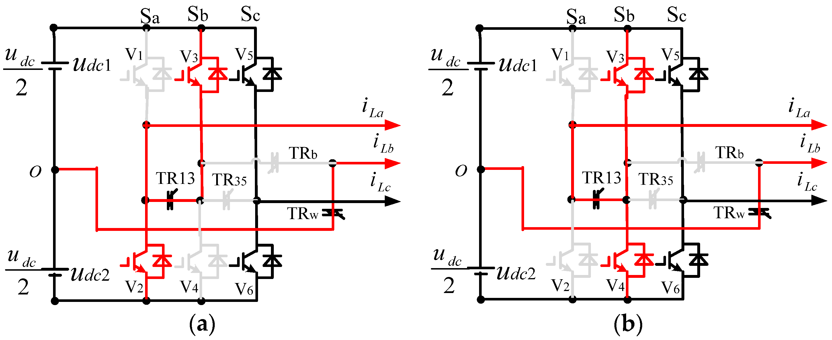
The topology structure of the proposed secondary reconfigurable inverter is shown in Figure 1. The inverter DC side voltage is provided by battery storage, which can ideally be considered as two DC sources with equal voltage value. V1–V6 are the power semiconductor devices IGBT, which constitute the three-phase inverter circuit. TR13, TR35, TRb and TRw are the TRIACS, which consist of the secondary reconfigurable circuit. A series of LC filters are used to inhibit higher harmonics and excessive short-circuit current. When the secondary reconfigurable inverter is operating normally, it is a TPSS inverter circuit.
The usual faults for the inverter are the short circuit and the open circuit of the power semiconductor devices. When the power semiconductor devices in the inverter encounter a short-circuit fault, the corresponding fast fuses will be fused, and the short-circuit fault is transformed into the open-circuit fault. The secondary reconfigurable inverter circuit is formed by cutting off the fault switches and connecting with the corresponding Triacs. When one or two of the power switch is faulty, the relationship among the corresponding Triacs and power switches are shown in Table 1.
In Table 1, consider cases 1 and 2 as examples. When the power switch V1 in the TPSS inverter circuit is faulty, turn on the Triacs TRwandTR13. Sending the pulse of V1 to be the pulse of V3 means that Tv3 = Tv1. The DC side voltage source can be considered as the b-phase bridge of the inverter, which constitutes the TPFS inverter circuit. V4 stops working. The reconstructed phases are Sa(V3, V2) and Sb(C1, C2). The reconstructing process is shown in Figure 2a, which is the first fault tolerance. Now the inverter is running in a fault-tolerant state. If V2 is also faulty, V3 and V4 construct phase Sa(V3, V4), sending the pulse of V2 to be the pulse of V4, Tv4 = Tv2, which is the secondary reconfiguration as shown in Figure 2b. Other cases have a similar switch process.
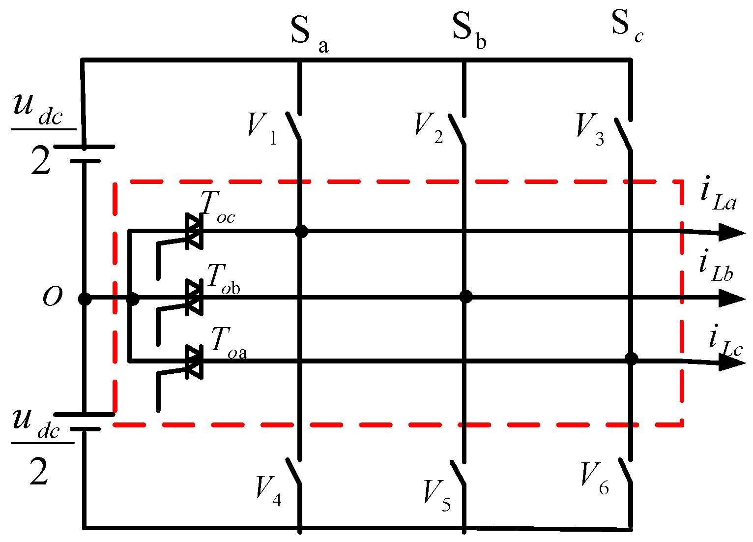
The traditional reconfigurable fault-tolerant inverter is shown in Figure 3.
From Figure 3, it can be seen that if one or two of the power switches in the traditional fault-tolerant inverter are faulty, the whole bridge needs to be removed. The relationship between the corresponding Triacs and power switches are shown in Table 2.
According to Table 2, the fault-tolerant space is small with just nine cases. The topology of the secondary reconfigurable inverter proposed in this paper greatly improves the fault-tolerant space. According to Table 1, the proposed secondary reconfigurable inverter has 21 fault-tolerant cases. Therefore, compared with the traditional inverter, the proposed secondary reconfigurable inverter has a broader fault-tolerant space. The fault-tolerant space of the proposed secondary reconfigurable inverter is improved greatly. Moreover, the control algorithm in a normal operation state needs to be converted into the control algorithm in the faulty state, which is complicated.

2.2. Analysis of the Fault Tolerant Inverter Operating Principle

2.2.1. Analysis of the Switching Mode

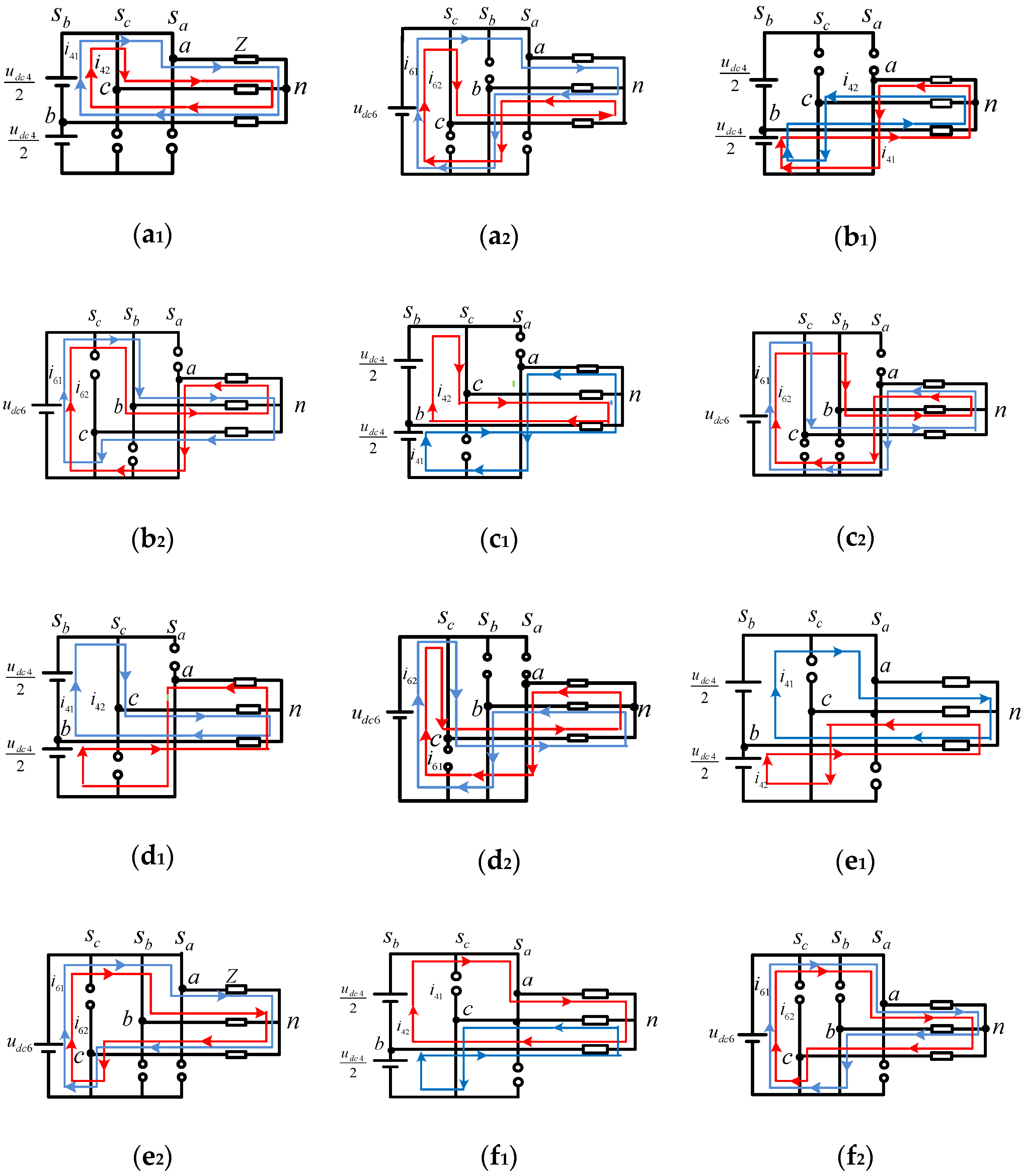
When the secondary reconfigurable inverter is running in the faulty state, the faulty power switch is removed. The remaining power switches of the two bridges can be reconfigured to keep operating. Each switching mode of the TPFS inverter has the corresponding switching mode as the TPSS inverter in a normal state. Varieties of switching modes and current paths of the TPSS inverter circuit and the reconfigured TPFS inverter circuit are shown in Figure 4.
In switching mode (a1), there are two current paths, i41 and i42, which both flow from the upper-half source of the DC-side source, which is equivalent to the condition that the b-phase lower-half bridge is connected and the upper bridge arm is cut off in the TPSS inverter circuit. At the moment, two current paths, i61 and i62, also exist in the TPSS inverter circuit.
According to the switching mode (a1) in Figure 4, the two current paths i41 and i42 satisfy the following equations, respectively.
i 41 = u d c 4 2 2 Z = u d c 4 4 Z
i 42 = u d c 4 2 2 Z = u d c 4 4 Z
Therefore the three-phase output voltages of the reconfigurable inverter circuit are
u a n 4 = i 41 Z = u d c 4 4
u c n 4 = i 42 Z = u d c 4 4
u b n 4 = ( i 41 + i 42 ) Z = u d c 4 2
In switching mode (a2), the two current paths i61 and i62 of the normal inverter circuit satisfy the following equations, respectively.
i 61 = u d c 6 2 Z
i 62 = u d c 6 2 Z
Then, the three-phase output voltages of the normal inverter circuit are defined by the following equations respectively.
u a n 6 = i 61 Z = u d c 6 2
u c n 6 = i 62 Z = u d c 6 2
u b n 6 = ( i 61 + i 62 ) Z = u d c 6
Let the three-phase output voltages of the reconfigurable inverter circuit be equal to the three-phase output voltages of the normal inverter circuit, respectively. Hence,
{ u a n 4 = u a n 6 u b n 4 = u b n 6 u c n 4 = u c n 6
That is to say,
u d c 4 = 2 u d c 6
Connecting Equation (12) with the Equations (1), (2), (6) and (7), it can be derived that the output current of the inverter satisfies the following equations
i 41 = i 61
i 42 = i 62
Similar results can be obtained in other switching modes, which are not repeated here. By setting the DC side voltage value of the reconfigurable inverter to be twice the DC-side voltage in the normal state, we can control the inverter according to the switching state shown in Table 1, no matter if the inverter is running in a faulty state or in a normal state. The normal output voltage and output current can be obtained in both states.

2.2.2. The Control Strategy for the Reconfigurable Inverter

When the power semiconductor devices of the secondary reconfigurable inverter are faulty, the TPSS inverter circuit is reconfigured as the TPFS inverter circuit. The relationship between the pulse signals produced by the SPWM (Sinusoidal Pulse Width Modulation) and the on–off states of each power semiconductor device is shown in Table 1. Tv1–Tv6 are the 6-channel modulation signals.
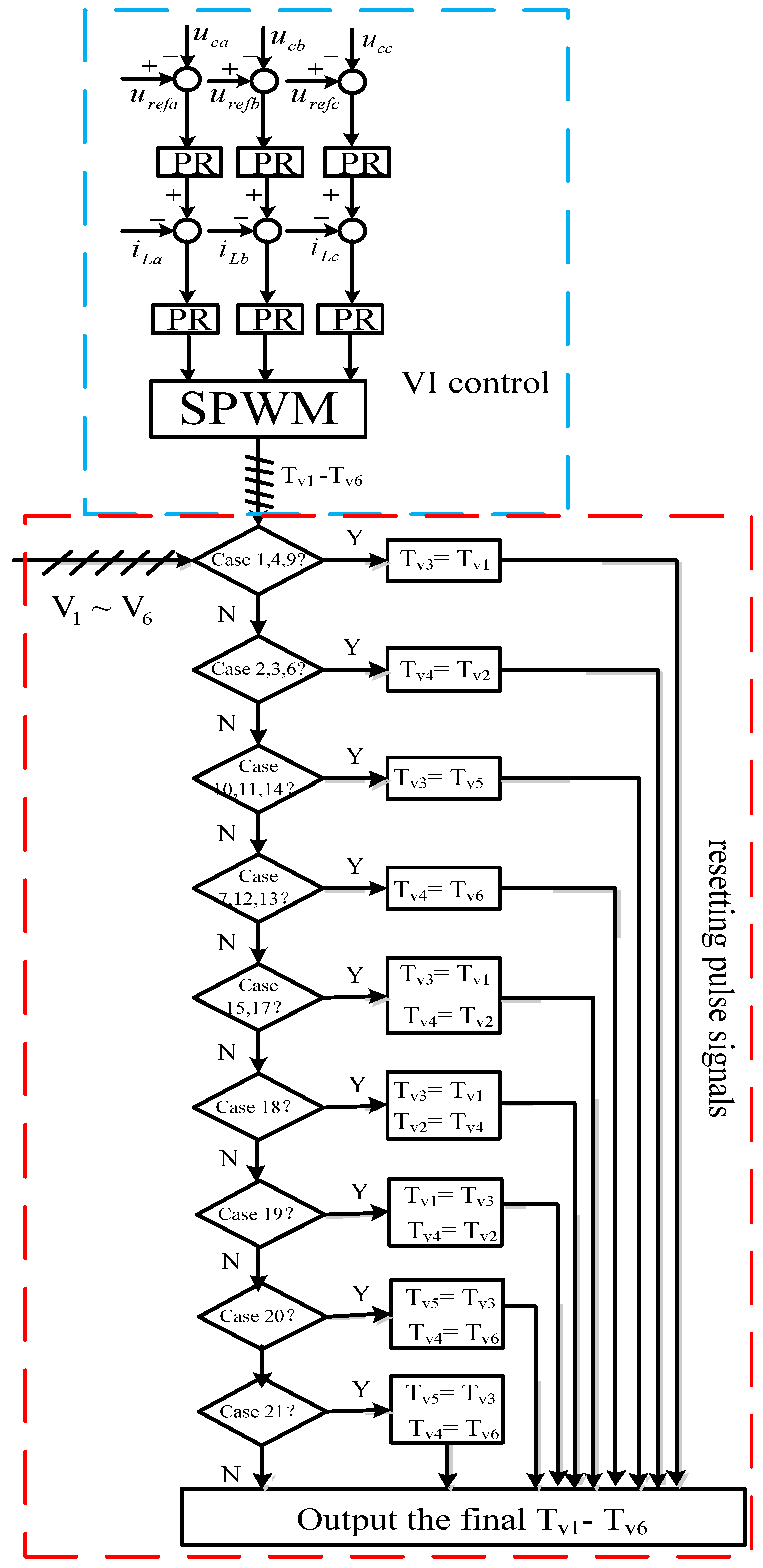
The switch-pulse-resetting algorithm is also proposed in this article. This article adopts the control strategy connecting the voltage–frequency control strategy with the switch-pulse-resetting algorithm. The flow figure of the control strategy is seen in Figure 5.
In Figure 5, the signals produced by VI control are put into SPWM, and then the initial 6-channel pulse signals Tv1–Tv6 are obtained by the SPWM. According to the on–off states of the 6 power semiconductor devices V1–V6, whether each pulse signal needs to alter or not is determined by the on–off states of 6 power semiconductor devices V1–V6. Finally, the device outputs the resetting pulse signals Tv1–Tv6 according to the red box in the Figure 5. There is no need for other cases to alter the initial pulse signals: Figure 5 shows that it need not alter the control algorithm when the system running from the normal state into the faulty state.

3. Results and Discussion

3.1. Simulation Results and Discussion

The circuit model of the secondary reconfigurable inverter shown in Figure 1 was built in MATLAB/Simulink platform to verify the feasibility and effectiveness of the proposed reconfigurable inverter in this article. This paper adopts the controlling strategy connecting the constant-voltage, constant-frequency control method and the switch pulse resetting algorithm.
The main parameters of the reconfigurable inverter applied in islanded micro-grid are shown the following Table 3.
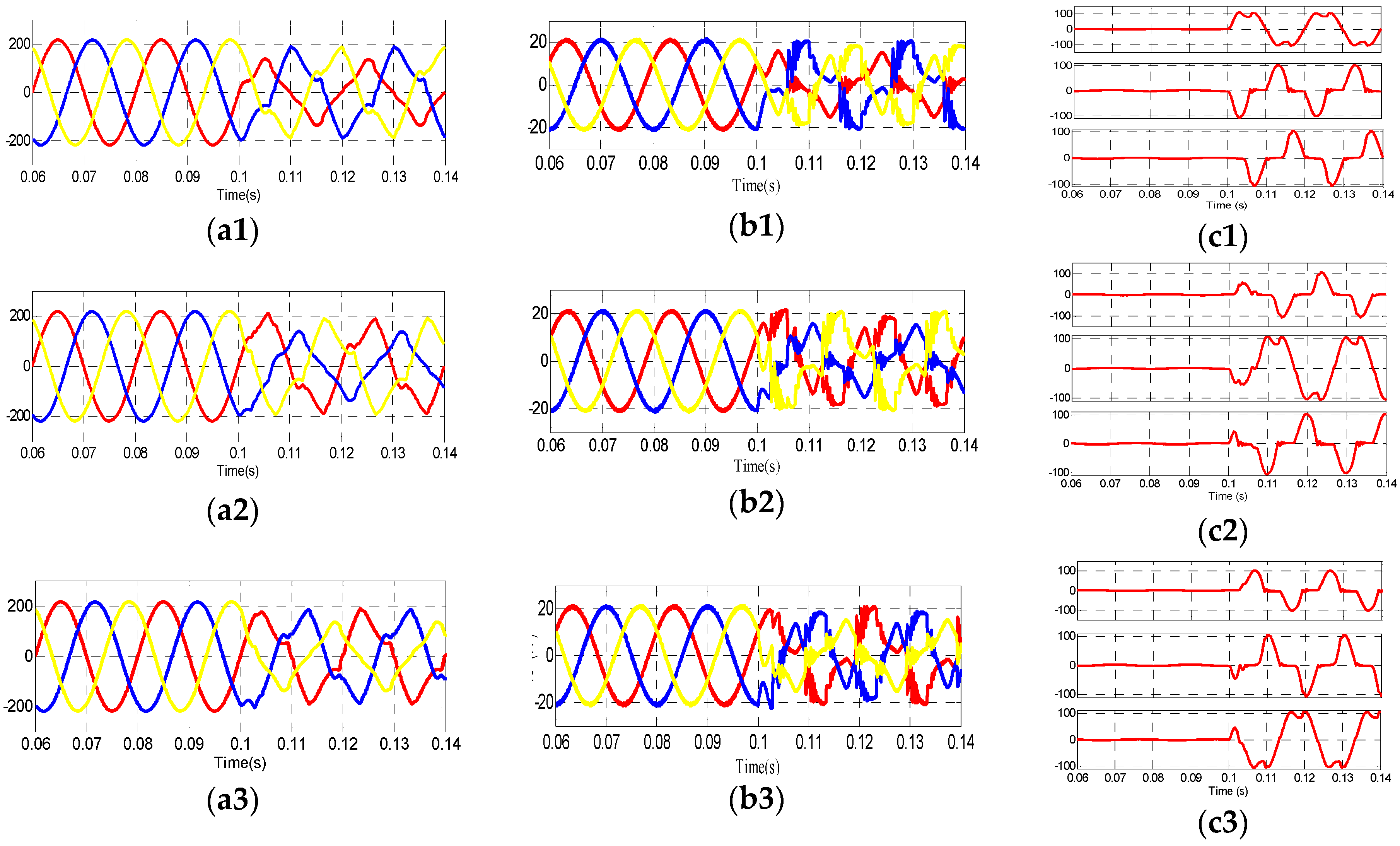
The simulation waveforms of the reconfigurable inverter applied to the islanded microgrid in the normal operating state and various faulty states are shown as follows. Set the system operating in normal state during 0–0.1 s and operating in the faulty state during 0.1–0.2 s.
The simulation results of the inverter without reconfigurable structure are shown in Figure 6, which include the waveforms of the output voltages, the output currents and the deviations between output voltages with reference voltages. Figure 7 shows the simulation results of the inverter with a reconfigurable structure.
When the DC side voltage is set as 400 V and without reconfigurable structure in the inverter, Figure 6a1,b1,c1 show output voltages, currents and deviations between the output voltage with the reference voltage corresponding to faulty phase a, respectively. Figure 6a2,b2,c2 show output voltages, currents and deviations between the inverter output voltage with the reference voltage corresponding to faulty phase b, respectively. Figure 6a3,b3,c3 show output voltages, currents and deviations between the inverter output voltage with the reference voltage corresponding to faulty phase c, respectively. It can be seen from the waveforms that the inverter voltages and the currents of the inverter are the expected standard sinusoidal waves when the inverter is running in the normal state at 0–0.1 s. Moreover, the deviation among the inverter output voltage with reference voltage is very small at about 3 V. After 0.1 s, the inverter is running in the faulty state. The inverter output voltage and output current are seriously distorted, and a three-phase imbalance appears. The deviation among inverter output voltage with reference voltage is too large.
Take case 1 in Table 1 as an example to verify the feasibility and validity of the proposed topology and the control algorithm in this simulation. The power switch V1 is faulty, and the inverter is reconstructed from TPSS to TPFS to be fault-tolerant. The DC voltage is set as 800 V in the reconfigurable inverter. Figure 7a–c are output voltages, currents and deviations between the output voltage with the reference voltage, respectively. All waveforms can be kept the same before and after the inverter is reconfigured because a power switch is broken at 0.1 s. If another power switch is faulty, the same output voltages and currents are obtained as the results in the first reconfiguration. Figure 7 represents the similar simulating waveforms of other cases in Table 1. That is to say, whether the inverter is reconfigured or not because of one or two power switches being broken, the output voltages and currents are similar to the reference voltages and currents. Therefore, the simulation results verify the feasibility and effectiveness of the proposed secondary reconfigurable inverter topology and control strategy.

3.2. Experimental Results and Discussion

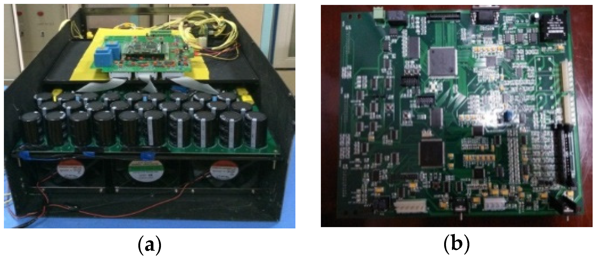
To further verify the feasibility and effectiveness of the proposed circuit topology of secondary reconfigurable inverter for the islanded microgrid, the experimental platform of the reconfigurable inverter was built. The system parameters were the same as the simulation parameters. DSP(digital signal processor) TMS320F2812 was used to generate pulses for the fault-tolerant inverter. Images of the experimental setups are shown in Figure 8. The main circuit board has a good and compact structural layout. The DC side voltages are provided by the rectifier. The loads are the resistors.
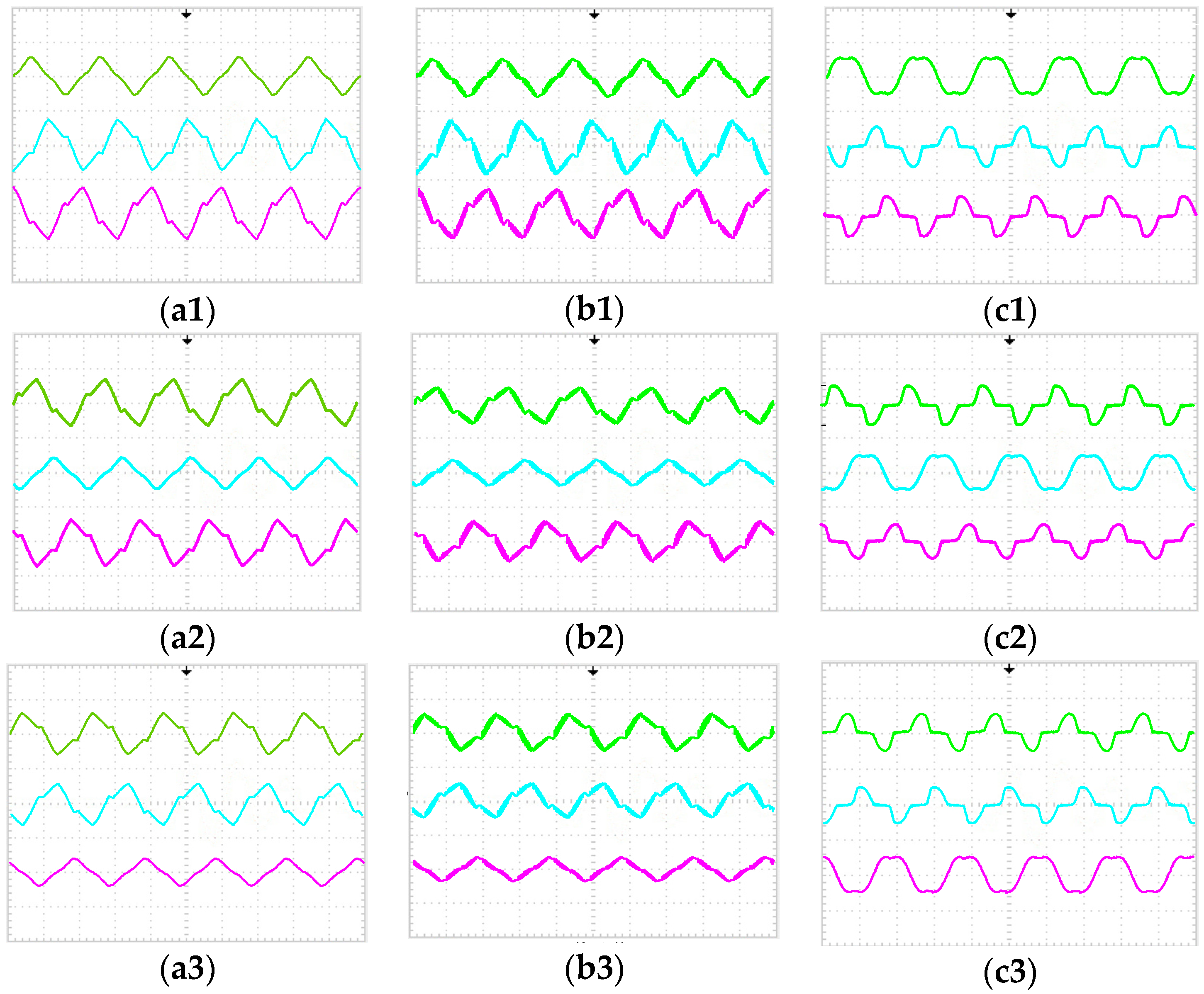
When the DC side voltage is set as 400 V in the non-reconfigurable inverter that is faulty, in phase a, phase b and phase c, the experimental results are shown in Figure 9. Figure 9a1–a3 show output voltages corresponding, respectively, to faulty phase a, b and c with the vertical axis 100 V/grid and horizontal axis 10 ms/grid. Figure 9b1–b3 show output currents corresponding, respectively, to faulty phase a, b and c with the vertical axis 30 A/grid and horizontal axis 10 ms/grid. Figure 9c1–c3 show the voltage deviations between output voltages and reference voltages corresponding, respectively, to faulty phase a, b and c with the vertical axis 50 V/grid and horizontal axis 10 ms/grid. This can be seen from the waveforms being distorted seriously and three-phase imbalance when the inverter is operating in a faulty state. The voltage deviations between output voltages and reference voltages are too large.
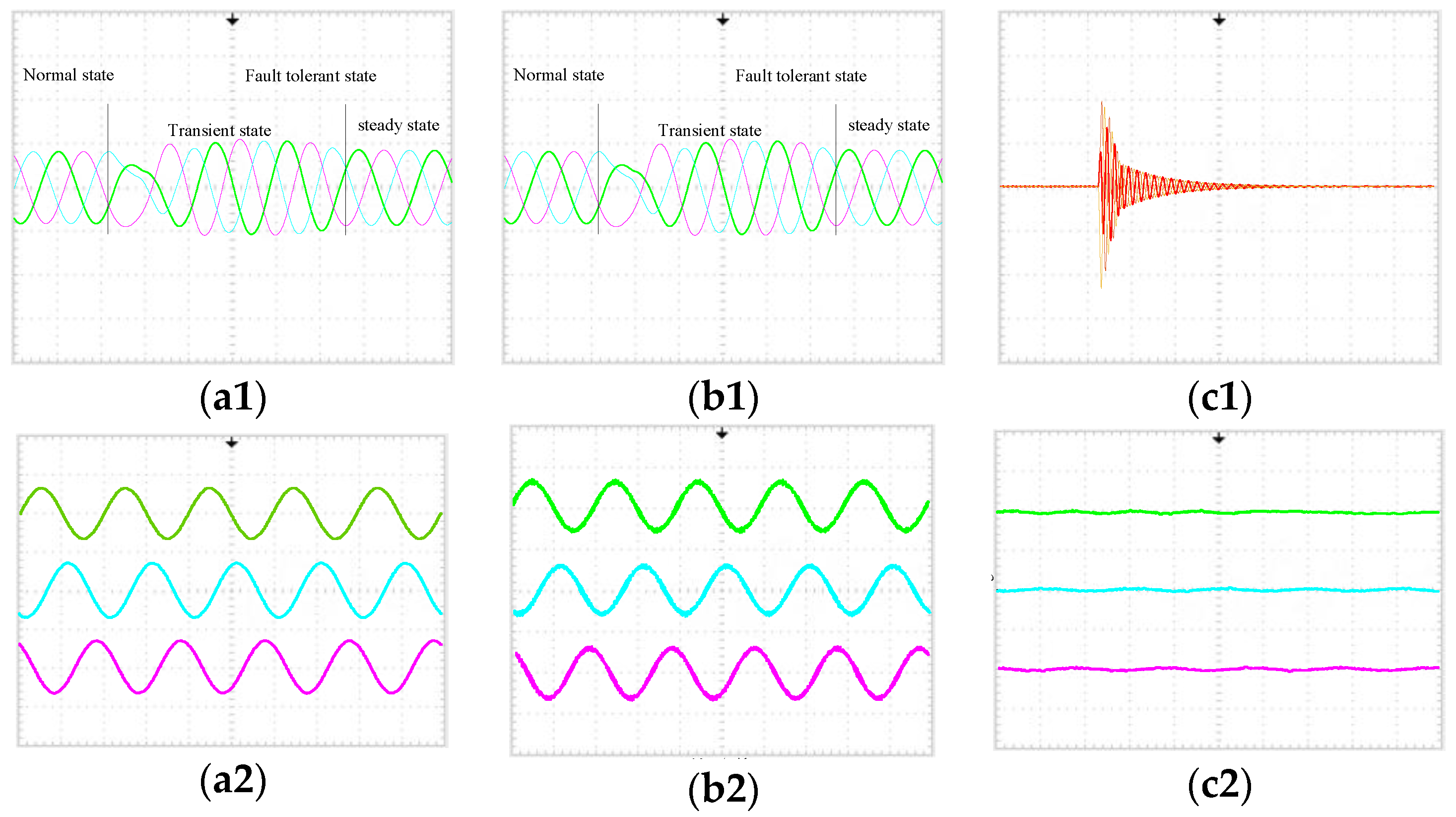
Take case 1 in Table 1 as an example to verify the feasibility and validity of the proposed topology and the control algorithm. The power switch V1 is faulty, and the inverter is reconstructed from TPSS to TPFS. Figure 10a1,a2 show output voltages corresponding to faulty phase a with the vertical axis 100 V/grid and horizontal axis 10 ms/grid. Figure 10b1,b2 show output currents corresponding to faulty phase a with the vertical axis 30 A/grid and horizontal axis 10 ms/grid. Figure 10c1,c2 show the voltage deviations between output voltages and reference voltages with the vertical axis 50 V/grid and horizontal axis 10 ms/grid. When the DC side voltage is set as 800 V in the reconfigurable inverter to be fault-tolerant, the experimental results of the changing process from a normal state to fault-tolerant state are shown in Figure 10a1,b1,c1. Since the DC side voltage satisfies all DC voltage conditions, it can be seen that the fault-tolerant waves are similar to the normal ones after the transient state. The inverter output voltages and output currents are standard sinusoidal waves. The deviation among inverter output voltage with reference voltage is small, and the steady experimental results are shown in Figure 10a2–c2. All the output waveforms after the inverter is reconstructed are similar to those in normal states. Other cases in Table 1 have similar results. Experimental results further verified the feasibility and validity of the proposed secondary reconfigurable topology and the control algorithm.

4. Conclusions

This article proposes a novel secondary reconfigurable inverter and the corresponding faul- tolerant control strategy. When the power semiconductor devices in the inverter are faulty, removing the faulty power semiconductor devices, the remaining power semiconductor devices and the DC source are remodeled to keep the inverter running. The fault-tolerant space is much larger than that of traditional inverter. This article has analyzed the relationship between the DC side voltages in a faulty state and in a normal state, given the corresponding control strategy and the switch-pulse-resetting algorithm. It need not change the control algorithm when the proposed reconfigurable inverter transforms the normal state into the faulty state. The simulation model was built in a normal state and various faulty states. The simulation and experimental results verify the feasibility and effectiveness of the proposed reconfigurable inverter topology structure and the control strategy.

Author Contributions

Y.L.: writing the manuscript and simulation; P.X.: simulation and editing; Y.C.: review and funding. All authors have read and agreed to the published version of the manuscript.

Funding

This research was funded by National Natural Science Foundation of China, Grant number 51507192 and 51677063.

Conflicts of Interest

The authors declare no conflict of interest.

References

  1. Abronzini, U.; Attaianese, C.; D’Arpino, M.; Di Monaco, M.; Tomasso, G. Steady-State Dead-Time Compensation in VSI. IEEE Trans. Ind. Electron. 2016, 63, 5858–5866. [Google Scholar] [CrossRef]
  2. Mehdi, F.F.; Alireza, R.; Mohsen, G. Stability Analysis and Decentralized Control of Inverter-Based AC Microgrid. Prot. Control Mod. Power Syst. 2019, 4, 65–86. [Google Scholar]
  3. Ballestín-Fuertes, J.; Muñoz-Cruzado-Alba, J.; Sanz-Osorio, J.F.; Hernández-Callejo, L.; Alonso-Gómez, V.; Morales-Aragones, J.I.; Gallardo-Saavedra, S.; Martínez-Sacristan, O.; Moretón-Fernández, Á. Novel Utility-Scale Photovoltaic Plant Electroluminescence Maintenance Technique by Means of Bidirectional Power Inverter Controller. Appl. Sci. 2020, 10, 3084. [Google Scholar] [CrossRef]
  4. Soukaina, E.D.; Loubna, L.; Mustapha, A.L. Sliding Mode Approach Applied to Sensorless Direct Torque Control of Cage Asynchronous Motor Via Multi-Level Inverter. Prot. Control Mod. Power Syst. 2020, 5, 166–175. [Google Scholar]
  5. Zhang, W.; Xu, D.; Enjeti, P.; Li, H.; Hawke, J.T.; Krishnamoorthy, H.S. Survey on Fault-Tolerant Techniques for Power Electronic Converters. IEEE Trans. Power Electron. 2014, 29, 6319–6331. [Google Scholar] [CrossRef]
  6. Longchang, W.; Houlei, G.; Guibin, Z. Modeling Methodology and Fault Simulation of Distribution Networks Integrated with Inverter-Based DG. Prot. Control Mod. Power Syst. 2017, 2, 370–378. [Google Scholar]
  7. Chen, J.; Shang, Y.; Chen, A.; Xing, X. Fault-Tolerant Control Strategies for T-Type Three-Level Inverters Considering Neutral-Point Voltage Oscillations. IEEE Trans. Ind. Electron. 2019, 66, 2837–2846. [Google Scholar] [CrossRef]
  8. Lu, B.; Sharma, S. A Literature Review of IGBT Fault Diagnostic and Protection Methods for Power Inverters. IEEE Trans. Ind. Appl. 2009, 45, 1770–1777. [Google Scholar] [CrossRef]
  9. Karimi, S.; Gaillard, A.; Poure, P.; Saadate, S. FPGA-Based Real-Time Power Converter Failure Diagnosis for Wind Energy Conversion Systems. IEEE Trans. Ind. Electron. 2008, 55, 4299–4308. [Google Scholar] [CrossRef]
  10. Naidu, M.; Gopalakrishnan, S.; Nehl, T. Fault-Tolerant Permanent Magnet Motor Drive Topologies for Automotive X-By-Wire Systems. IEEE Trans. Ind. Appl. 2010, 46, 841–848. [Google Scholar] [CrossRef]
  11. Errabelli, R.R.; Mutschler, P. Fault-Tolerant Voltage Source Inverter for Permanent Magnet Drives. IEEE Trans. Power Electron. 2011, 27, 500–508. [Google Scholar] [CrossRef]
  12. De Lillo, L.; Empringham, L.; Wheeler, P.; Khwan-On, S.; Gerada, C.; Othman, M.; Huang, X. Multiphase Power Converter Drive for Fault-Tolerant Machine Development in Aerospace Applications. IEEE Trans. Ind. Electron. 2009, 57, 575–583. [Google Scholar] [CrossRef]
  13. Liu, G.; Xu, Z.; Xue, Y.; Tang, G. Optimized Control Strategy Based on Dynamic Redundancy for the Modular Multilevel Converter. IEEE Trans. Power Electron. 2014, 30, 339–348. [Google Scholar] [CrossRef]
  14. Blaabjerg, F.; Neacsu, D.; Pedersen, J. Adaptive SVM to compensate DC-link voltage ripple for four-switch three-phase voltage-source inverters. IEEE Trans. Power Electron. 1999, 14, 743–752. [Google Scholar] [CrossRef]
  15. Hu, S.; Liu, G.; Jin, N.; Guo, L. Constant-Frequency Model Predictive Direct Power Control for Fault-Tolerant Bidirectional Voltage-Source Converter with Balanced Capacitor Voltage. Energies 2018, 11, 2692. [Google Scholar] [CrossRef] [Green Version]
  16. Zhu, C.; Zeng, Z.; Zhao, R. Comprehensive Analysis and Reduction of Torque Ripples in Three-phase Four-switch Inverter-fed PMSM Drives Using Space Vector Pulse-width Modulation. IEEE Trans. Power Electron. 2016, 32, 1. [Google Scholar] [CrossRef]
  17. Li, W.; Xuan, S.; Gao, Q.; Luo, L. Investigation of a Four-Switch Four-Leg Inverter: Modulation, Control, and Application to an IPMSM Drive. IEEE Trans. Power Electron. 2018, 34, 5655–5666. [Google Scholar] [CrossRef]
  18. Zeng, Z.; Zheng, W.; Zhao, R.; Zhu, C.; Yuan, Q. Modeling, Modulation and Control of the Three-Phase Four-Switch PWM Rectifier under Balanced Voltage. IEEE Trans. Power Electron. 2015, 31, 1. [Google Scholar] [CrossRef]
  19. Zeng, Z.; Zheng, W.; Zhao, R. Space-Vector-Based Hybrid PWM Strategy for Reduced DC-Link Capacitor Current Stress in the Post-Fault Grid-Connected Three-Phase Rectifier. IEEE Trans. Ind. Electron. 2016, 63, 1. [Google Scholar] [CrossRef]
  20. Zeng, Z.; Zheng, W.; Zhao, R.; Zhu, C.; Yuan, Q. The Comprehensive Design and Optimization of the Post-Fault Grid-Connected Three-Phase PWM Rectifier. IEEE Trans. Ind. Electron. 2015, 63, 1629–1642. [Google Scholar] [CrossRef]
  21. Xia, C.; Li, Z.; Shi, T. A Control Strategy for Four-Switch Three-Phase Brushless DC Motor Using Single Current Sensor. IEEE Trans. Ind. Electron. 2009, 56, 2058–2066. [Google Scholar] [CrossRef]
  22. Klima, J. Analytical Investigation of an Induction Motor Fed from Four-Switch VSI with a New Space Vector Modulation Strategy. IEEE Trans. Energy Convers. 2006, 21, 832–838. [Google Scholar] [CrossRef]
  23. Kim, J.; Hong, J.; Nam, K. A Current Distortion Compensation Scheme for Four-Switch Inverters. IEEE Trans. Power Electron. 2009, 24, 1032–1040. [Google Scholar] [CrossRef]
  24. Wang, R.; Zhao, J.; Liu, Y. A Comprehensive Investigation of Four-Switch Three-Phase Voltage Source Inverter Based on Double Fourier Integral Analysis. IEEE Trans. Power Electron. 2011, 26, 2774–2787. [Google Scholar] [CrossRef]
  25. Correa, M.B.D.R.; Jacobina, C.B.; Da Silva, E.R.C.; Lima, A.M.N. A General PWM Strategy for Four-Switch Three-Phase Inverters. IEEE Trans. Power Electron. 2006, 21, 1618–1627. [Google Scholar] [CrossRef]
  26. Xia, C.; Wu, D.; Shi, T.; Chen, W. A Current Control Scheme of Brushless DC Motors Driven by Four-Switch Three-Phase Inverters. IEEE J. Emerg. Sel. Top. Power Electron. 2017, 5, 547–558. [Google Scholar] [CrossRef]
  27. Zaky, M.S.; Metwaly, M.K. A Performance Investigation of a Four-Switch Three-Phase Inverter-Fed IM Drives at Low Speeds Using Fuzzy Logic and PI Controllers. IEEE Trans. Power Electron. 2017, 32, 3741–3753. [Google Scholar] [CrossRef]
  28. Dasgupta, S.; Mohan, S.; Sahoo, S.K.; Panda, S.K. Application of Four-Switch-Based Three-Phase Grid-Connected Inverter to Connect Renewable Energy Source to a Generalized Unbalanced Microgrid System. IEEE Trans. Ind. Electron. 2012, 60, 1204–1215. [Google Scholar] [CrossRef]
  29. Tsang, K.-M.; Chan, W.-L. Single DC source three-phase multilevel inverter using reduced number of switches. IET Power Electron. 2014, 7, 775–783. [Google Scholar] [CrossRef]
  30. Jin, N.; Hu, S.; Gan, C.; Ling, Z. Finite States Model Predictive Control for Fault-Tolerant Operation of a Three-Phase Bidirectional AC/DC Converter Under Unbalanced Grid Voltages. IEEE Trans. Ind. Electron. 2018, 65, 819–829. [Google Scholar] [CrossRef]
  31. Ceballos, S.; Pou, J.; Zaragoza, J.; Robles, E.; Villate, J.L.; Martin, J.L. Fault-Tolerant Neutral-Point-Clamped Converter Solutions Based on Including a Fourth Resonant Leg. IEEE Trans. Ind. Electron. 2010, 58, 2293–2303. [Google Scholar] [CrossRef]
  32. Ceballos, S.; Pou, J.; Robles, E.; Gabiola, I.; Zaragoza, J.; Villate, J.; Boroyevich, D. Three-Level Converter Topologies With Switch Breakdown Fault-Tolerance Capability. IEEE Trans. Ind. Electron. 2008, 55, 982–995. [Google Scholar] [CrossRef]
  33. Correa, P.; Pacas, M.; Rodríguez, J. Modulation Strategies for Fault-Tolerant Operation of H-Bridge Multilevel Inverters. 2006 IEEE Int. Symp. Ind. Electron. 2006, 2, 1589–1594. [Google Scholar] [CrossRef]
  34. Liu, Y.; Li, D.; Jin, Y.; Wang, Q.; Song, W. Research on Unbalance Fault-Tolerant Control Strategy of Modular Multilevel Photovoltaic Grid-Connected Inverter. Energies 2018, 11, 1368. [Google Scholar] [CrossRef] [Green Version]
  35. Choi, U.-M.; Lee, K.-B.; Blaabjerg, F. Diagnosis and Tolerant Strategy of an Open-Switch Fault for T-Type Three-Level Inverter Systems. IEEE Trans. Ind. Appl. 2013, 50, 495–508. [Google Scholar] [CrossRef]
  36. Choi, U.-M.; Blaabjerg, F.; Lee, K.-B. Reliability Improvement of a T-Type Three-Level Inverter with Fault-Tolerant Control Strategy. IEEE Trans. Power Electron. 2014, 30, 2660–2673. [Google Scholar] [CrossRef]
  37. Zhou, D.; Li, Y.; Zhao, J.; Wu, F.; Luo, H. An Embedded Closed-Loop Fault-Tolerant Control Scheme for Nonredundant VSI-Fed Induction Motor Drives. IEEE Trans. Power Electron. 2016, 32, 3731–3740. [Google Scholar] [CrossRef]
  38. Zhang, W.; Xu, D.; Wang, H. Fault Analysis and Fault-Tolerant Design for Parallel Redundant Inverter Systems in Case of IGBT Short-Circuit Failures. IEEE J. Emerg. Sel. Top. Power Electron. 2018, 6, 2031–2041. [Google Scholar] [CrossRef]
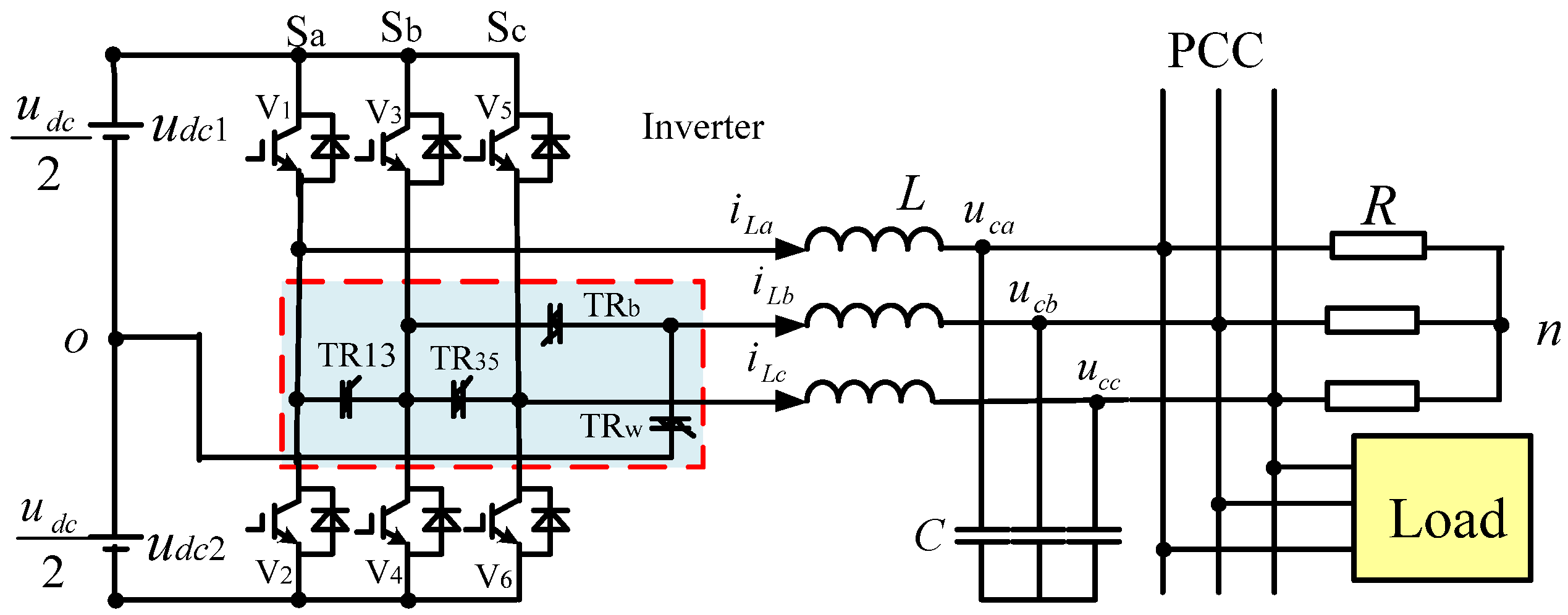
Figure 1. The topology structure of the proposed secondary reconfigurable inverter.
Applsci 10 07021 g001
Figure 2. The secondary reconfiguring process of the inverter: (a) the first reconfiguration; (b) the secondary reconfiguration.
Applsci 10 07021 g002
Figure 3. The traditional reconfigurable fault-tolerant inverter.
Applsci 10 07021 g003
Figure 4. Switching modes and current paths (Sa, Sc) for the faulty state and (Sa, Sb, Sc) for the normal state: (a1) (1,1); (a2) (1, 0, 1); (b1) (0,0); (b2) (0,1, 0); (c1) (0,1); (c2) (0,1, 1); (d1) (0,1); (d2) (0,0, 1); (e1) (1,0); (e2) (1,1, 0); (f1) (1,0); (f2) (1,0, 0).
Applsci 10 07021 g004
Figure 5. The proposed control strategy flow figure.
Applsci 10 07021 g005
Figure 6. Simulation results of the non-reconfigurable inverter: (a1) output voltages under faulty phase a; (a2) output voltages under faulty phase b; (a3) output voltages under faulty phase c; (b1) currents under faulty phase a; (b2) currents under faulty phase b; (b3) currents under faulty phase c; (c1) voltage deviations under faulty phase a; (c2) voltage deviations under faulty phase b; (c3) voltage deviations under faulty phase c.
Applsci 10 07021 g006
Figure 7. Simulation results of the reconfigurable inverter under faulty phase a: (a) output voltages; (b) currents; (c) voltage deviations.
Applsci 10 07021 g007
Figure 8. The experiment setup: (a) the main circuit board; (b) DSP; (c) the rectifier; (d) the load.
Applsci 10 07021 g008aApplsci 10 07021 g008b
Figure 9. The experimental results of the non-reconfigurable inverter (a1) output voltages under faulty phase a; (a2) output voltages under faulty phase b; (a3) output voltages under faulty phase c; (b1) currents under faulty phase a; (b2) currents under faulty phase b; (b3) currents under faulty phase c; (c1) voltage deviations under faulty phase a; (c2) voltage deviations under faulty phase b; (c3) voltage deviations under faulty phase c.
Applsci 10 07021 g009
Figure 10. The experimental results of the reconfigurable inverter under faulty V1 (a1) dynamic output voltages; (a2) steady output voltages; (b1) dynamic currents; (b2) steady currents; (c1) dynamic voltage deviation; (c2) steady voltage deviation.
Applsci 10 07021 g010
Table 1. Secondary reconfigurable inverter switching status.
CaseFirst FaultOnReconfigured PhasesSecond FaultReconfigured PhasesSwitch Pulse Resetting
0/TRb////
1V1TRw and TR13Sa (V3, V2) Sb (C1, C2)//Tv3 = Tv1
2V1TRw and TR13/V2Sa (V3, V4) Sb (C1, C2)Tv4 = Tv2
3V2TRw and TR13Sa (V1, V4) Sb (C1, C2)//Tv4 = Tv2
4V2TRw and TR13/V1Sa (V3, V4) Sb (C1, C2)Tv3 = Tv1
5V3TRwSb (C1, C2)///
6V3TRw and TR13 V2 Sa (V1, V4) Sb (C1, C2)Tv4 = Tv2
7V3TRw and TR35/V6 Sc (V5, V4) Sb (C1, C2)Tv4 = Tv6
8V4TRwSb (C1, C2)///
9V4TRw and TR13 V1 Sa (V3, V2) Sb (C1, C2)Tv3 = Tv1
10V4TRw and TR35 V5Sc (V3, V6) Sb (C1, C2)Tv3 = Tv5
11V5TRw and TR35Sc (V3, V6) Sb (C1, C2)//Tv3 = Tv5
12V5TRw and TR35 V4Sc (V3, V6) Sb (C1, C2)Tv6 = Tv4
13V6TRw and TR35Sc (V5, V4) Sb (C1, C2)/ Tv4 = Tv6
14V6TRw and TR35 V3Sc (V5, V4) Sb (C1, C2)Tv5 = Tv3
15V1 and V2TRw and TR13Sa (V3, V4) Sb (C1, C2)//Tv3 = Tv1,Tv4 = Tv2
16V3 and V4TRwSb (C1, C2)//
17V5 and V6TRw and TR35Sc (V3, V4) Sb (C1, C2)//Tv3 = Tv1,Tv4 = Tv2
18V1 and V4TRw and TR13Sa (V3, V2) Sb (C1, C2)//Tv3 = Tv1,Tv2 = Tv4
19V2 and V3TRw and TR13Sa (V1, V4) Sb (C1, C2)//Tv1 = Tv3,Tv4 = Tv2
20V3 and V6TRw and TR35Sc (V5, V4) Sb (C1, C2)//Tv5 = Tv3,Tv4 = Tv6
21V4 and V5TRw and TR35Sc (V3, V6) Sb (C1, C2)//Tv3 = Tv5,Tv6 = Tv4
Table 2. The traditional inverter switching status.
CaseFaultOnReconfigured Phases
0///
1V1TocSa (C1, C2)
2V4TocSa (C1, C2)
3V2TobSb (C1, C2)
4V5TobSb (C1, C2)
5V3ToaSc (C1, C2)
6V6ToaSc (C1, C2)
7V1 and V4TocSa (C1, C2)
8V2 and V5TobSb (C1, C2)
9V3 and V6ToaSc (C1, C2)
Table 3. The main parameters of the simulation model.
Main ParametersValue
Reference voltage amplitude Um\V220
Reference voltage frequency f\Hz50
DC side voltage u d c \V400/800
IGBT switch frequency\kHz10
Output side filter inductance L0\mH1.2
Output side filter capacitance C0\µF4000
Load resistance value RL12
Load inductance value LL\mH1.4
Kp of PR0.6
KR of PR500