Review

Twistronics in Graphene, from Transfer Assembly to Epitaxy

Center for Spintronics and Quantum Systems, State Key Laboratory for Mechanical Behavior of Materials, Xi’an Jiaotong University, Xi’an 710049, China
*
Author to whom correspondence should be addressed.
Appl. Sci. 2020, 10(14), 4690; https://doi.org/10.3390/app10144690
Submission received: 31 May 2020 / Revised: 4 July 2020 / Accepted: 6 July 2020 / Published: 8 July 2020
(This article belongs to the Special Issue Fundamentals and Recent Advances in Epitaxial Graphene on SiC)

Abstract

:
The twistronics, which is arising from the moiré superlattice of the small angle between twisted bilayers of 2D materials like graphene, has attracted much attention in the field of 2D materials and condensed matter physics. The novel physical properties in such systems, like unconventional superconductivity, come from the dispersionless flat band that appears when the twist reaches some magic angles. By tuning the filling of the fourfold degeneracy flat bands, the desired effects are induced due to the strong correlation of the degenerated Bloch electrons. In this article, we review the twistronics in twisted bi- and multi-layer graphene (TBG and TMG), which is formed both by transfer assembly of exfoliated monolayer graphene and epitaxial growth of multilayer graphene on SiC substrates. Starting from a brief history, we then introduce the theory of flat band in TBG. In the following, we focus on the major achievements in this field: (a) van Hove singularities and charge order; (b) superconductivity and Mott insulator in TBG and (c) transport properties in TBG. In the end, we give the perspective of the rising materials system of twistronics, epitaxial multilayer graphene on the SiC.

Graphical Abstract

1. Introduction

Since the year 2004, graphene [1] has been a focus of condensed matter physics and materials science due to their superior physical properties, especially those showing potential applications in next generation electronics and optoelectronics. Recently, the twistronics, which refers to the studies of the electronic properties of two-dimensional layered structures with particular twist angles between the layers, has become a fast rising new branch of the field in regard to two dimensional (2D) material.
The fascinating research on 2D materials experienced three sequential stages in its development, each represented by a new degree of freedom in the sense of material structure. Stage 1 is represented by a real 2D system, e.g., freestanding graphene, which allows the discovery of various properties superior to the 3D or quasi-2D systems; stage 2 is represented by tailor-made 2D heterojunctions, which give rise to a variety of van der Waals stacking systems and stage 3 is represented by a twist angle between the neighboring layers, which facilitates the fine tuning of electronics structures and magically induces strong correlation phenomenon at “magic” twist angles, e.g., twistronics.
The concept “twistronics” was first introduced by S. Carr et al. in a theory paper [2] to discuss general approaches to calculate the electronic structure of arbitrarily twisted bilayer 2D materials. Prior to that, researchers had already worked on this topic and discovered or predicted a number of interesting properties of twisted bilayer graphene (TBG), for example, van Hove singularity [3,4,5,6], a possible flat band at “magic” angles [7,8,9,10,11]. The rise of twistronics was boosted in 2018, by Jarillo-Herrero’s group’s experimental discovery of superconductivity [12] and Mott insulator [13] on the graphene device with almost the exact “magic” twist angle, which was fabricated by the so called “tear and stack” transfer assembly technique, as demonstrated in Figure 1a. Many other interesting properties, like a topological Chern insulator [14,15,16], local charge order [17,18,19,20], as well as those of twisted multilayer 2D heterostructures [11,21,22,23], have been reported soon after. Currently this field has become one of the hottest in the frontier. However, if the twistronics would one day come to practical electronics devices, it is worth putting effort into realizing such a material system by more feasible methods, like epitaxial growth.
In this paper, we review the advances of this field, in the aspects of its band structure theory, transport properties and local electronic properties. Additionally, we will discuss the perspective of twistronics on epitaxial material systems, particularly epitaxial graphene on wide band semiconductor SiC (as in Figure 1b), aiming at promoting the application of twistronics in electronic devices based on the strong correlation effects, potentially useful in the next generation integrated circuits for quantum computing.

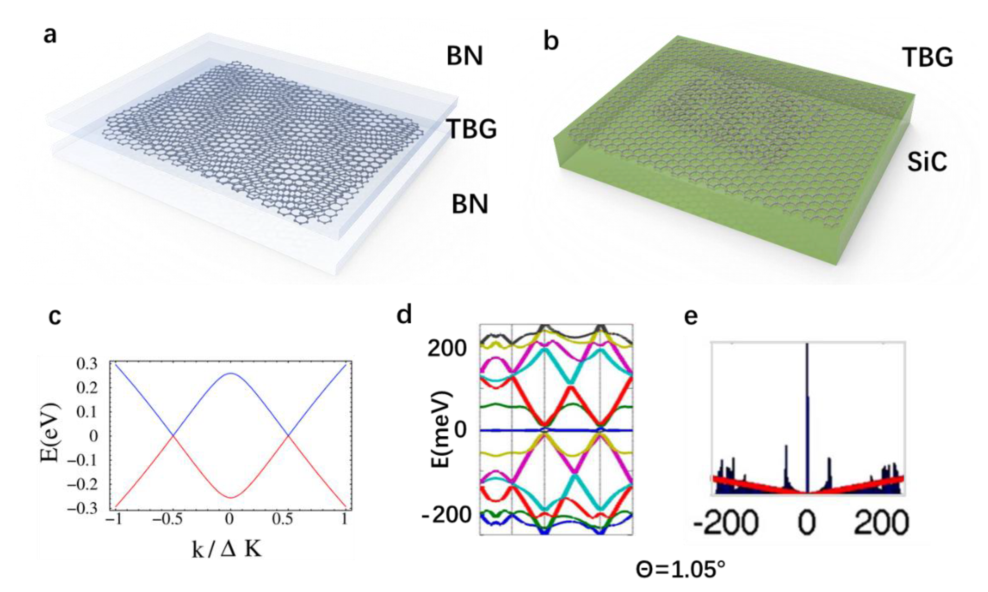
2. Electronic Structure of Twist Bilayer Graphene

When two layers of graphene are stacked up, they are in Bernal (AB) stacking or AA stacking when the crystal orientations of both layers are aligned, which is usually the case for grown crystals due to thermodynamics. However, when the bilayer structure is fabricated by transferring the exfoliated monolayers, the crystal orientations are mostly misaligned with a twist angle θ, which could be well controlled to the accuracy of 0.1° recently [25,26]. Such a twisted bilayer forms a super structure called the moiré pattern, with lattice constant d = a ( 2 sin ( θ 2 ) ) 1 , where a = 0.246 nm, i.e., the lattice constant of graphene. In each moiré unit cell, there are three high symmetry spots, AA, AB and BA, named after the local stacking geometry.
A. H. Castro Neto and coworkers [24] studied the electronic structure of the such unique geometry of the bilayer graphene as early as in 2007. Within the framework of the continuum approximation on a small twist angle model, they found that the linear dispersion at low energy and the Dirac cones structure remain in the twisted bilayer, as shown in Figure 1c, but with a significant reduction of the Fermi velocity for very small twist angles. Such results imply the twist angle could be a significant parameter that has a profound effect on the electronic structure of the bilayer graphene.
A theoretical breakthrough was made by R. Bistritzer and A. H. MacDonald in 2011 [8]. They unambiguously pointed out that the Fermi velocity at the Dirac point vanishes at a series of magic twist angles, e.g., θ = 1.05°, when the dispersionless flat bands (also called moiré bands) are formed around the charge neutrality point, as shown in Figure 1d. Such a flat band contributes to a sharp peak to the density of state, which is shown in Figure 1e. They also remarked that the electron–electron interaction in the magic twist angle systems could give rise to strong correlation effects. E. Suárez Morell et al. [7] mentioned the link between superconductivity and the flat bands of twisted graphene, although they give the critical angle of 1.5° that is a little deviated from the magic angle.
From the view of the band structure, comparing with gapless monolayer graphene, it is two superlattice bandgaps that are next to the upper and bottom sub flat band due to the effect of interlayer hybridization in TBG. According to theoretical calculation [7,9,27], when the twist angle is increasing, and away from the first magic angle, the position of the gap would shift to higher energy until being disappeared as the two sub minibands become wider. Such twist angle tuned gaps are valuable for the application in the optoelectronic device, for example, B. Deng, et al. [28] demonstrated the gate-tunable photoresponse in the mid-infrared wavelength range of 5–12 μm in 1.81° TBG. Additionally, a number of recent optoelectronic works based on bigger twist angle TBG were done [29,30,31,32].
Another interesting feature in the electronic structure of the TBG is the doubled van Hove singularity in the density of states that generally exists at arbitrary angles TBG as a consequence of the saddle points at two emerging Dirac cones [6,9]. Additionally, a number of theory works have investigated the band topology [27,33,34,35,36,37,38] in the magic angle TBG system recently.
Although many of the interesting predicted properties are yet to be verified or investigated in detail by experiments, the flat bands have been directly observed in experiments, e.g., angle-resolved photoemission spectroscopy (ARPES) [39]. And the flat band related unconventional superconductivity and Mott insulating states have been discovered by Pablo Jarillo-Herrero’s group [12,13] in 2018. In the following sections the major experimental achievements on TBG will be discussed.

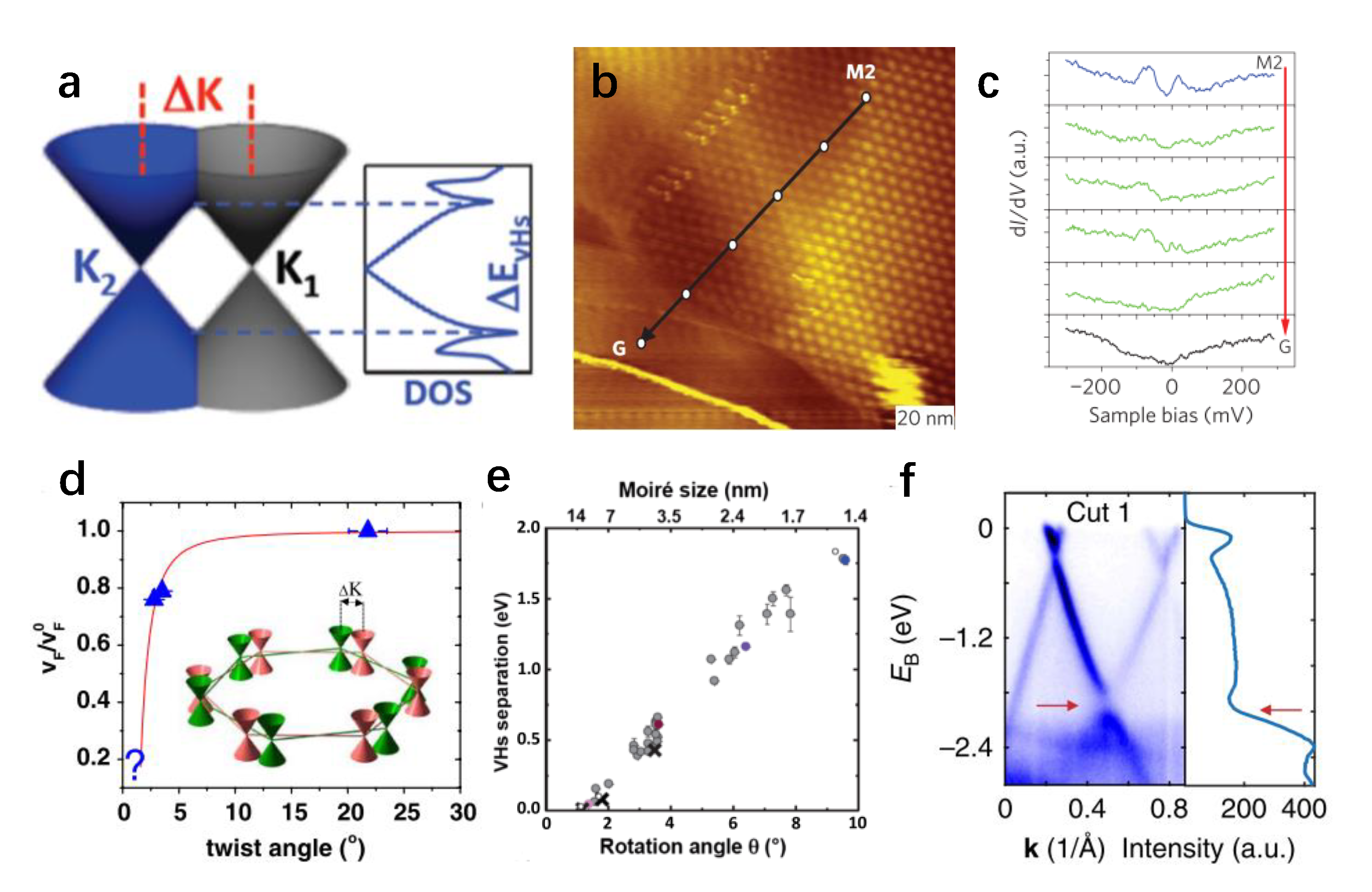
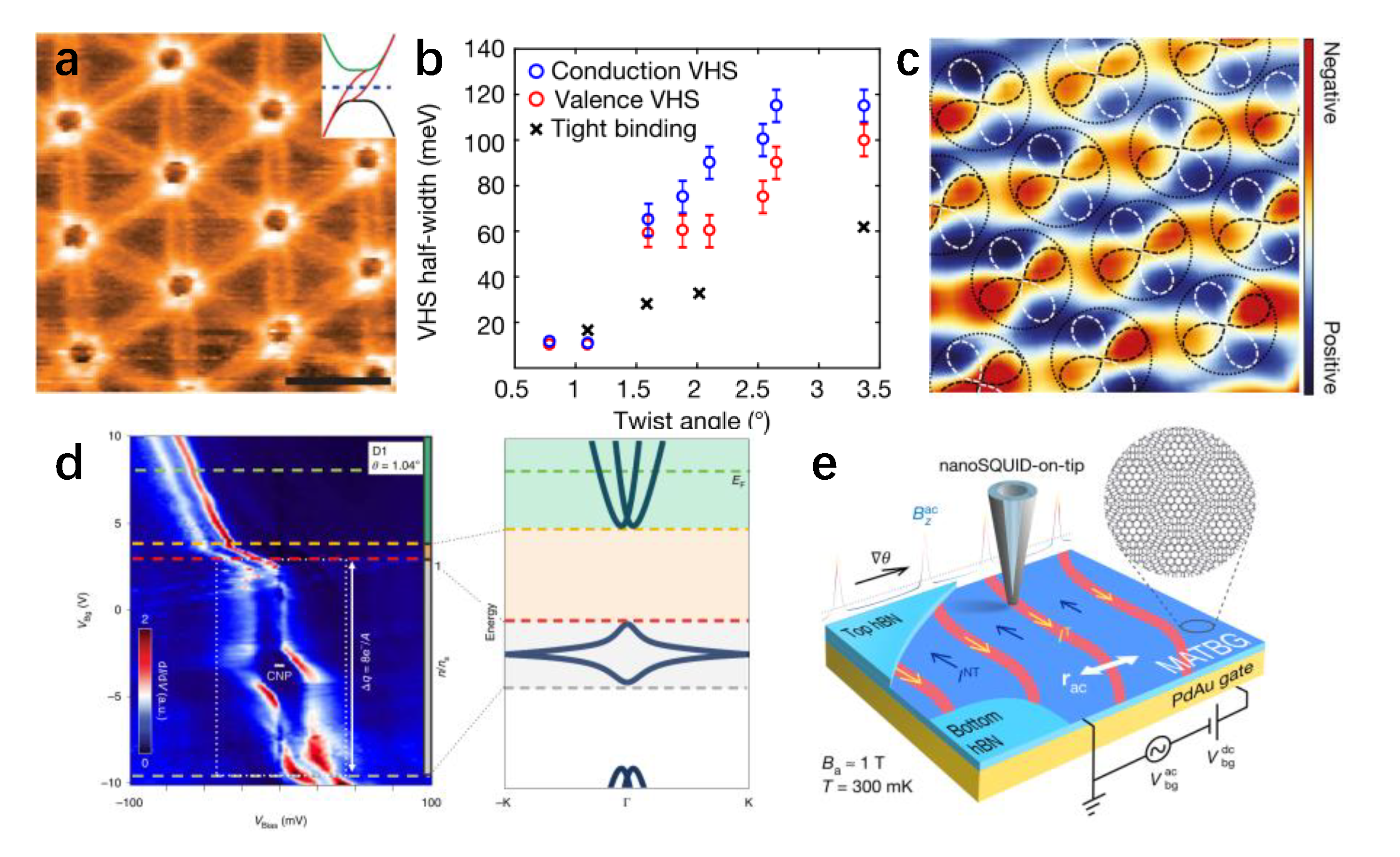
3. Van Hove Singularities

Van Hove singularities (VHS) in the density of states are attractive properties of TBG, since strong correlation effects like superconductivity, ferromagnetism and the charge density wave could be induced when the system Fermi level is tuned to van Hove singularities energy levels. The VHS of TBG at low energy come from the saddle points formed when the Dirac cones of each graphene layer cross and merge together, as shown in Figure 2a [40]. Obviously, the VHS are always in a pair and are symmetric to the charge neutral point (CNP) in energy levels.
Actually, van Hove singularities are the first unique and well-studied phenomenon in TBG. The experimental studies on the moiré flat band, superconductivity, etc., are later inspired by the discovery of van Hove singularities. The earliest experimental work of the van Hove singularity in TBG are carried out by E. Y. Andrei‘s group, with scanning tunneling microscopy (STM) [3]. They have found a pair of sharp peaks symmetrical to the charge neutrality point in the scanning tunneling spectroscopy (STS) taken on the highly oriented pyrolytic graphite (HOPG) surface with the moiré pattern, as shown in Figure 2b,c. With the help of the theory, they could assign these peaks to the saddle points of the merged two Dirac cones, e.g., VHS levels. Later, they investigated the influence of the twist angle to the van Hove singularity energy levels by investigating chemical vapor deposition (CVD) grown TBG samples with various twist angles [4]. By measuring the Landau level positions under a high magnetic field, the Fermi velocity vF could be deduced. It is found that the vF of large twist angle TBG is similar to monolayer graphene, while the vF of the small angle TBG is significantly lower, for example, vF = 0.87 × 10⁶ m/s when θ = 1.16°; vF = 1.1 × 10⁶ m/s for monolayer graphene [41], as shown in Figure 2d.
On the twisted multilayer graphene epitaxial grown on 6H-SiC( 000 1 ¯ ), J.-Y. Veuillen’s group systematically investigated the VHS levels by measuring the STS on samples with varying twist angles [40], as shown in Figure 2e. They have found that Δ E V H S = 2 ħ v F Γ K s i n ( θ / 2 ) 2 t θ , where vF is the Fermi velocity, ΓK is the wave vector of the Dirac point in monolayer graphene and tθ is the modulus of the amplitude of the main Fourier components of the interlayer potential for monolayer graphene. L. He’s group [5] reported similar results on TBG samples grown on Rh foil, and reveal the coupling between epitaxial graphene and substrate could also influence the energy levels of VHS. These results are verified again by J. Yin et al. [30] on epitaxial 19.1° TBG on Cu foil by direct observation of the saddle point on the valance band of TBG by μ-ARPES, as shown in Figure 2f.

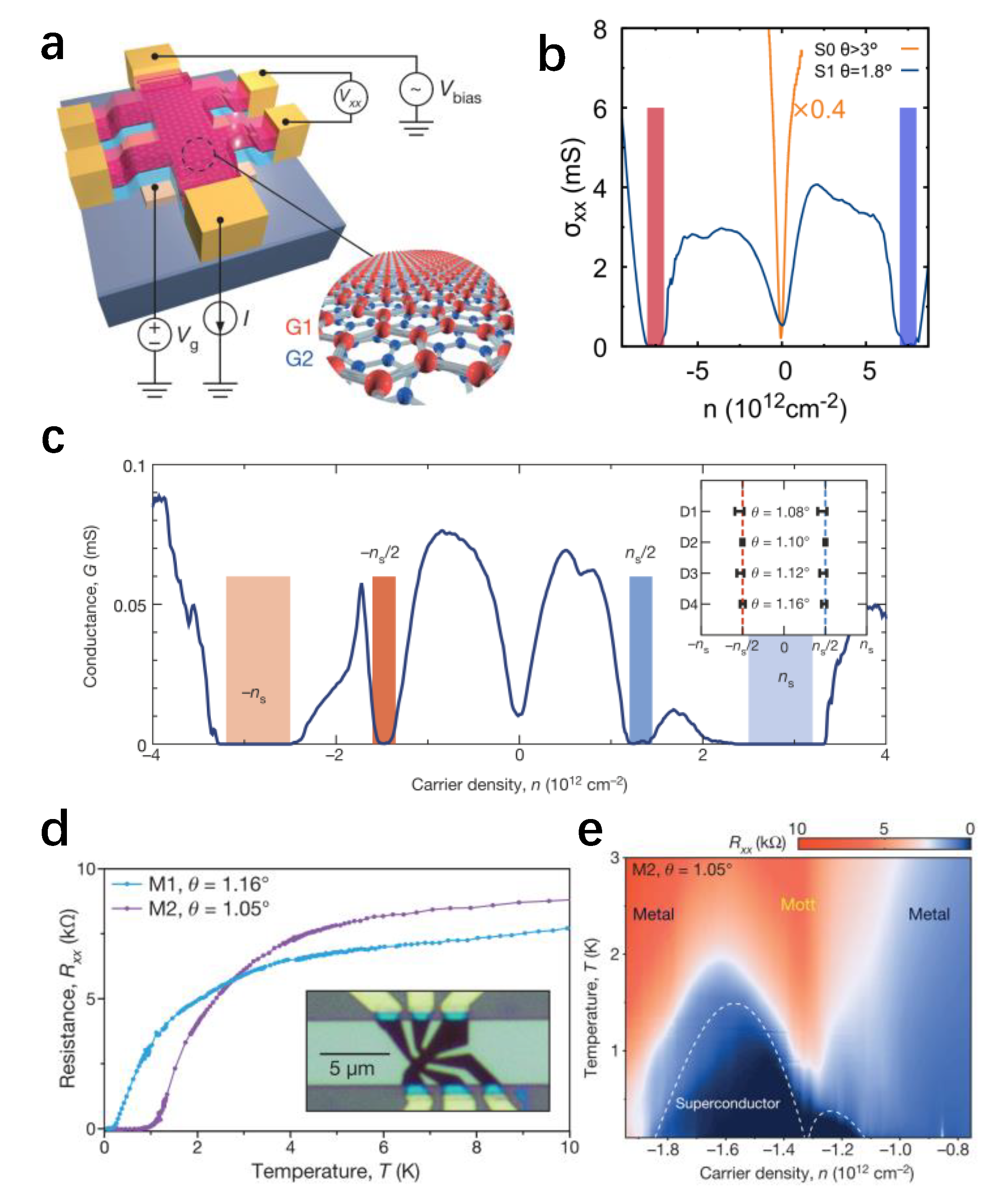
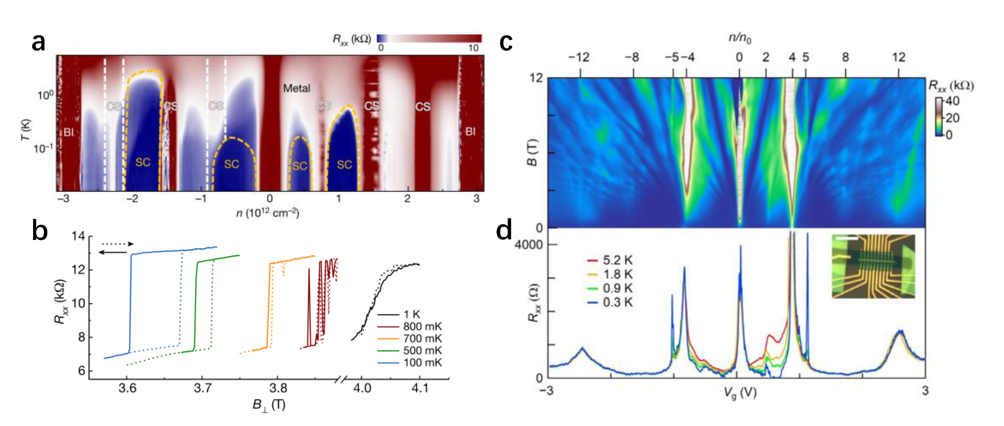
4. Mott Insulator and Superconductivity

The superconductivity in TBG with the magic angle was firstly reported by Y. Cao et al. in 2018 [12], and confirmed by many other researchers soon after [14,42,43]. The superconducting behavior of TBG is largely similar to the doped Mott insulator, similar to unconventional high TC superconductor. Although it is well known that the monolayer graphene is a zero gap semiconductor with the highest mobility [44,45,46] among all the materials, Y. Cao et al. surprisingly discovered the insulating behavior in the TBG in 2016 [26]. They had successfully fabricated dual-gate hall bar devices (Figure 3a) with two TBG of different twist angles. The one with a twist angle > 3° shows a normal V-shape dip in the conductivity-carrier density curve, as shown in Figure 3b, which indicates the normal behavior of conductivity increases with carrier density around the zero density (charge neutral) point. However, in the small angle sample θ = (2.0 ± 0.5) °, they observe two insulating states, which are symmetric on both sides of the charge neutrality point. Such insulating states are suppressed when the temperature increases. Interestingly, the total density of the states required to fill up the insulating gaps, n = 7.5 × 1012 cm−2, is 4 times of the mini Brillouin zone area, indicating two fold valley degeneracy and two fold spin degeneracy. Therefore, they could derive the unit cell area of the moiré superlattice to be 4/n = 53.3 nm2, which correspond to the twist angle of θ = 1.8°, matching the target value of θ = (2.0 ± 0.5)°.
The insulating behavior could be well explained by the flat band in magic angle TBG, as introduced in Section 1. Basically, when the Fermi level crosses the flat band, the dynamic energy of electron is limited by the width of the flat band. The Bloch electron in flat band would have a very large effective mass, and thus the Coulomb interaction between electrons would dominate their behavior, i.e., Mott insulator at low temperature. Additionally, due to the combination of valley degeneracy and spin degeneracy, the flat band is fourfold degeneracy.
In 2018, Y. Cao et al. [13] verified the Mott insulating states of TBG by measuring devices with twist angles carefully controlled to 1.1°, close to the first magic angle. The full filling condition is four electrons per moiré unit cell, corresponding to a carrier density ns (in this work ns = 2.7 × 1012 cm−2). It was found that the insulating states not only appear at the charge neutral point (n = 0) and the full filling condition (n = ns), but also at the half filling condition (n = ±ns/2), as shown in Figure 3c. Additionally, by measuring the Shubnikov–de Haas oscillation frequency fSdH, they deduced that the degeneracy was to be 4 at charge neutrality and 2 at the half-filling states, and suggested the halved degeneracy of the Fermi pockets is related to the spin–charge separation. These results are unambiguous proof of Mott-like correlated behavior at half-filling. In a back to back paper on the same journal, Y. Cao et al. reported unconventional superconductivity in the same material system, as shown in Figure 3d, which was realized by back gate tuned electrostatic doping into the TBG slightly away from the correlated insulating state [12]. They observed tunable zero-resistance states, i.e., superconductivity, in two TBG devices with critical temperature of 1.7 K and 0.5 K respectively. Both devices show a maximum critical field of about 70 mT. The temperature and magnetic field–carrier density phase diagram demonstrate two dome-shaped superconducting phase regions approximate to both sides of the half-filling Mott-insulator region, as in Figure 3e. Such behavior of magic angle TBG is very similar to that of cuprates superconductors.
These works immediately inspired enormous attention to the TBG systems, both experimental and theoretical [14,42,47,48,49,50,51,52,53,54,55,56,57,58,59]. Due to the fourfold degeneracy of the moiré flat band, one can define a filling factor ν = n/n0 = 4n/ns (n0 is the carrier density for one electron per moiré unit cell). It is expected that insulating states appears when ν is the integer and superconducting exists between them. Indeed, X. Lu et al. reported that on a more accurate (θ = 1.1 ± 0.02°) magic angle TBG device, the insulating state appears at the integer filling factor positions, as shown in Figure 4a [14]. The temperature–carrier density phase diagram shows superconductivity up to 3 K around ν ≈ −2. Surprisingly, there are also three new superconducting domes at much lower temperatures, close to the ν = 0 and ν = ±1 insulating states. Moreover, at ν = −1, when the perpendicular magnetic field is higher than 3.6 T, the insulating state exhibits a sharp hysteretic resistance and the longitudinal resistance saturated at about 13 kΩ (Figure 4b). These details imply orbital magnetism and a non-zero Chern number induced by a possible field-driven phase transition at low temperature. E. Codecido et al. [42] reported an insulating state at a filling factor as high as 12 in the TBG with a twist angle of 0.93°, as shown in Figure 4c,d, which is surprising since at such a high filling condition the Fermi level has reached the dispersing bands. M. Yankowitz et al. [56] induced superconductivity in TBG with twist angle θ = 1.27°, larger than the first magic angle, by varying the interlayer spacing with hydrostatic pressure [60]. These superconducting (SC) domes are almost next to the correlated insulate states region in the B–T phase diagram, similar to the effect of the doping of the Mott insulator and implying the strong correlation effect between the electrons on the flat band in special filling. However, some theoretical works attributed the superconductivity in TBG to phonon driven [48,51].
In the above cases, the “tear and stack” technique were adopted by most of the groups to the fabricated magic angle twisted bilayer graphene device. This method [25,26] utilizes the van der Waals force between different materials to transfer graphene on different substrates. Precisely controlling the twist angle in the method is the key to realize the desired magic angle twisted bilayer graphene device. This is controlled by an accurate micro-manipulation stage and monitored by optical microscopy for confirming the twist angle in situ. Besides, in Y. Cao and X. Lu’s case, they both rotated the separated graphene pieces purposefully by an angle slightly larger than the desired twist angle, owing to the high risk of relaxation of the twist angle to random lower values. Furthermore, X. Lu, et al. further carried out a mechanical cleaning process for squeezing the trapped blister out and releasing the local strain. More details and other different synthetic methods of twisted graphene can refer to this review paper [61], which introduced the method more comprehensively.
Moreover, in the early transport measurement of TBG devices, the filling is mainly tuned by the back gate, as shown in Figure 3a. One should note that the back gate not only changes the carrier density, but also changes the electric displacement field. Theory suggests the vertical electrical field would influence the band structure of the bilayer graphene. To eliminate this effect, researchers normally employ a symmetric due gate design for the devices. More details of the physics in such systems are still yet to be further investigated on more sophisticated devices.

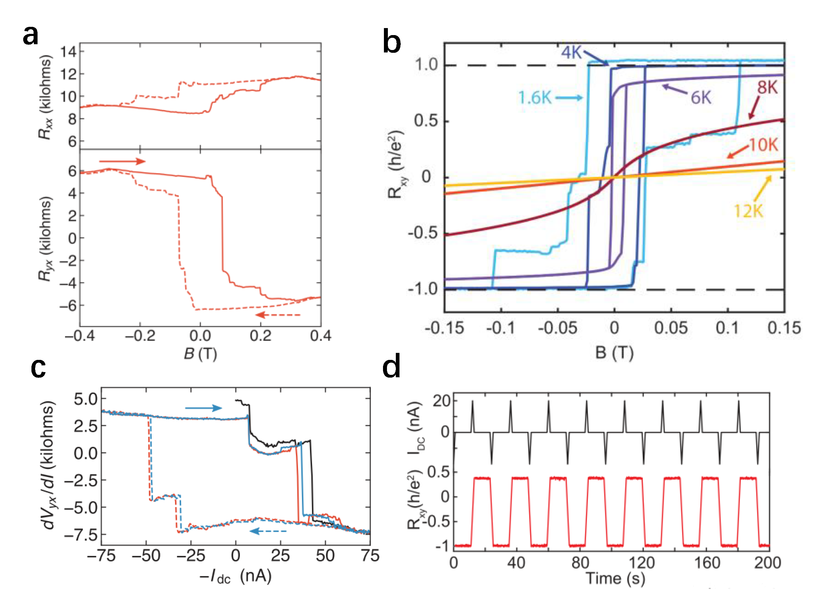
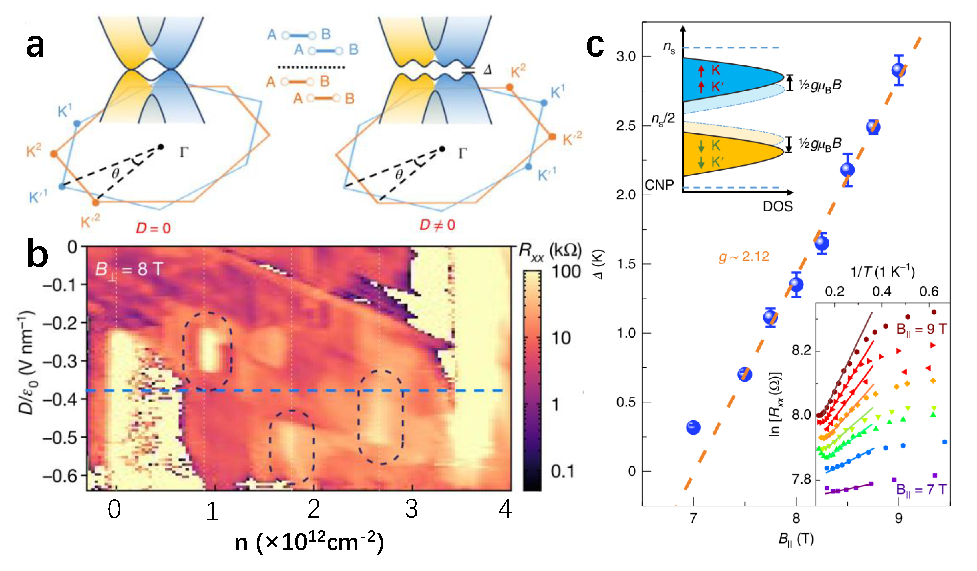
5. Ferromagnetism and Quantum Anomalous Hall Effect

The ferromagnetic state in TBG has been predicted by L. A. Gonzalez-Arraga et al. [62] in 2017 and antiferromagnetism was suggested as well [63]. Basically, fine tuning of the band filling would lift the degeneracy, and thus induce ferromagnetism in the system. For example, the spin symmetry and valley symmetry could be partially or completely broken in the 1/4, 1/2 and 3/4 filling. A. L. Sharpe et al. reported that the transport measurement shows hysteretic behavior with respect to an applied out-of-plane magnetic field B below 3.9 K, near the 3/4 filling of the moiré band in a TBG Hall bar device [64], as shown in Figure 5a. Considering the absence of transition metal and other heavy elements, the large amorous hall signal in TBG is surprising. This suggests spin and valley symmetries in the correlated insulated states are spontaneously broken. M. Serlin et al. also found the ferromagnetic state near the 3/4 filling in TBG devices [16]. The Hall resistivity is hysteretic, with a critical field of several tens of mT. At low temperature, lateral resistance Ryx quickly saturated at quantum resistivity h/e2 along with a low longitudinal resistivity Rxx < 1 kΩ, as shown in Figure 5b, which reveals a topological insulating state with Chern number = 1, similarly to the result by X. Lu et al. [14]. These results again indicate a quantum anomalous Hall (QAH) state by spontaneously broken time-reversal symmetry of the moiré band. Additionally, they both found the quantum anomalous Hall state can be switched on/off by a low direct current [16,64], as shown in Figure 5c,d, providing a possibility for functional devices.
This unusual magnetism in TBG, revealed by the anomalous Hall effect, cannot be explained by a trivial reason like adsorbed impurities or defects. Due to the absence of the d electron or f electron, the unusual magnetism at the 1/4 filling can be attributed to a field stabilized orbital magnetic state [14,65]. Additionally, the certainly potential ferromagnetic topological insulator, found at the 3/4 filling, is explained by spin or valley symmetry broken from the flat band. A series of theoretical works have attempted to find the reason of the electrically controllable magnetism [58,66,67,68,69] and the origin of the Chern number in TBG by calculating the topology of the flat band [34,35,37]. To better understand the magnetism experimentally, these spin or valley polarized states, which are around the AA region as suggested by the theory, need to be verified by performing more detailed local probe characterization.

6. Local Probe Measurement of TBG

Although the transport measurement already revealed many fascinating properties of TBG systems, one should note that the published results sometime are puzzling or contradicting to each other, for example, different determination to the insulating states at a certain filling to the band [13,42,64]; disagreed positions of the superconducting states in the phase diagram [12,14] and different critical magnetic field or critical temperature values [12,56]. These contradictions are mainly attributed to the unavoidable variation in device fabrication, local inhomogeneity or twist angle disorder. To avoid these deviations in the measurement that are carried out on a relatively large area, a local probe measurement that could zoom in to the individual moiré unit cell would be very helpful.
Due to the atomic resolution STM measurements on TBG, L. Yin et al. [70] observed the one-dimensional conducting channels locating at the edges of the domain wall between the AB and BA regions; S. Huang et al. [71] observed a double-line network of enhanced density of states on TBG with the moiré unit cell lattice constant of about 50 nm, as shown in Figure 6a. The density of the state is enhanced only when the gap was opened by applying a positive electric field, suggesting topologically protected helical edge states on the network. On the TBG samples with varying twist angles from 0.79° to 3.48°, A. Kerelsky et al. [19] detected the VHS features in STS spectra. They also found that the half-width of each individual VHS is minimized at the magic angle, as shown in Figure 6b, which means the electron correlations are maximized.
The influences of the electron–electron correlation interaction to the local electronic structure and local charge ordering are also very suitable for scanning probe measurement. By taking STS on the AA region of the moiré unit cell in TBG with the magic angle, Y. Xie et al. [20] studied the flat band peak position under different filling conditions. It was found that in the fully filled or empty condition, the shift of the flat band peak is proportional to the density of states (DOS) at the Fermi level, as shown in Figure 6d, indicating that the electron correlation is weak; while in the partial filling condition, an abrupt distortion of the spectra that cannot be explained by the mean-field model has been observed, indicating that a strong correlation effect is indeed playing a crucial role. Such a conclusion is also supported by the STS measurement on a similar system by Y. Choi et al. [17]. In addition, Y. Choi et al. observed an enhanced flat band peak splitting, which was attributed to exchange interactions. Furthermore, the strong correlation effect could also induce a stripe charge order, as reported by Y. Jiang et al. [18], as shown in Figure 6c.
Besides the scanning tunneling microscope, the nanoscale on-tip scanning superconducting quantum interference device (SQUID-on-tip) [73] is a powerful tool to study the local magnetic properties at high spatial resolution. Recently, A. Uri et al. [72] investigated the influence of local θ variation on the Landau levels in the quantum Hall states in magic angle TBG, at an ultra-high precision of 0.002° with SQUID-on-tip, as shown in Figure 6e. It was found that the correlated states being fragile with the twist-angle disorder, and the in-plane electron fields generated by the gradients of θ would affect the phase diagram of correlated superconducting states.

7. Twisted Multilayer Graphene

Apart from the gating as a major tool to tune the correlated states in TBG, the number of layers is also a knob for tuning. Actually, correlation effects also exist in the multilayer graphene with or without the twist angle, for example, the twisted double-bilayer graphene (TDBG) [21,74,75,76,77] formed between twisted AB stacking bilayer graphene. It is well known that the AB stacking bilayer graphene has parabolic bands touching at low energies close to the K point, and the gap opening at the charge neutral point could be induced under electric displacement fields, as shown in Figure 7a. Theory suggests that strong electron–electron interaction may occur in such a TDBG system at the 1/2 and1/4 filling of the flat band [78].
Indeed, a number of experimental works show evidence that the correlated insulate states exist in TDBG. Y. Cao et al. recently investigated the response of the correlated states to magnetic fields, perpendicular or in-plane [75]. At B = 8 T, the correlated insulate state at 1/2 ns shifts to a bigger D region in the n-D map, and the 1/4 ns insulate state shifts to a lower D region, as shown in Figure 7b. At the paralleled magnetic field, no such strong shift is observed at all fractional filling. In the evolution of the thermally activated gap of the 1/2 ns state, they find a g-factor of g|| ≈ 1.5 for the in-plane magnetic field, closer to g = 2 that corresponds to electron spin contribution, rather than g ≈ 3.5 for the out of plane magnetic field. These results suggest that the correlated states are spin-polarized. C. Shen et al. obtained an effective g factor of 2.12 by fitting the thermal activation gap according to the Zeeman effect in in-plane magnetic field [74], as shown in Figure 7c, which indicates spin polarization at half-filling. X. Liu et al. also reported the ferromagnetic order and superconductivity at 1/2 filling in TDBG [77]. Additionally, they surprisingly observed that the superconductivity is enhanced in the low in-plane magnetic field region, revealed by a 50% increase of critical temperature as B|| increases from 0 to about 0.3 T, again suggesting unusual spin-polarized electron pairing [77].
On an ABC stacking trilayer graphene with the 1/4 or 1/2 filling of the flat band, G. Chen et al. observed the Mott-insulating state [79], superconductivity [80], ferromagnetism and Chern insulator [15], as shown in Figure 8a–c. By applying the vertical field, they observed splitting of the low energy band and suppressing of the high energy flat band, indicating correlation due to Coulomb repulsion. L. Yin et al. reported Landau level spectroscopy measurements of ABC-stacked twisted trilayer graphene on graphite, and observed an approximately linear magnetic-field scaling of valley splitting and spin splitting, as shown in Figure 8d, which is attributed to a strong many-body correlation effect [81]. Additionally, by increasing the number of layers and complexity of the stack order, more twisted multilayer graphene come up in experiment [22,82,83] and theory [23,65,84,85,86], thus more fascinating properties are yet to be explored.

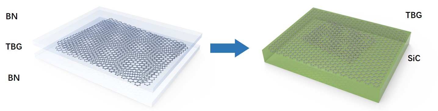
8. Twistronics in Epitaxial Graphene on SiC

So far, the materials for twistronics studies are dominated by transfer assembly of exfoliated graphene, mono- and bi-layer. Due to its great precision, the tear and stack method [25,87,88] of transfer assembly enables the successful fabrication of desired magic angle TBG devices. On the other hand, future application of twistronics would demand mass production of TBG based devices, and thus require more efficient and economically available method for the production of TBG materials. The epitaxial graphene on wide band semiconductor SiC stands out as a very promising candidate, due to its natural compatibility with the semiconductor industry. Therefore, more attention should be paid to SiC supported epitaxial graphene. (See Figure 9)
As early as in 1974, A. J. Van Bommel, et al. already reported the ring shape Low Energy Electron Diffraction (LEED) pattern on graphitized SiC( 000 1 ¯ ) [93], which now we know is multi-layer graphene with rotational domains of varying orientations. M. Naitoh et al. also observed many large and small domains with various periodicities at 6H-SiC( 000 1 ¯ ) surfaces [94], which can be explained as moiré patterns formed on two graphene layers with different twist angles. On the 4H-SiC( 000 1 ¯ ) substrate, J. Hass, et al. reported that multilayer graphene grown on the carbon terminated SiC surface contains three rotational domains, rotated by the 30 ± 2.2° direction, characterized by LEED as shown in Figure 9a, and these rotational stacking faults could be largely tuned by the annealing temperature [89].
Since the pioneer work by the W. A. de Heer group in 2004 [95], lots of attention has been focused on the SiC(0001), i.e., Si terminated face, due to the high quality of the self-limited epitaxial graphene up to two layers. Meanwhile, many surface science studies, by means of auger electron spectroscopy (AES) [90,96], XPS [97,98,99], LEEM [100], STM [101], etc., were carried out on the epitaxial graphene on the SiC( 000 1 ¯ ), i.e., C terminated face. It was confirmed that the C-face could provide multilayer epitaxial graphene with a thickness up to 10 s of nanometers, as shown in Figure 9b. The precise number of layers could be determined in situ [102]. Additionally, the technique to control the thickness and domain size of C-face graphene has also been developed. K.V. Emtsev et al. [91], J. L. Tedesco et al. [103] and G. R. Yazdi et al. [104] reported the Ar atmosphere annealing method that could provide micrometer sized single domains, as shown in Figure 9c. The epitaxial graphene on C-face SiC tends to exhibit a variety of domain with various twist angles, as shown in Figure 9d, which could provide rich research objects simultaneously.
In recent years, the physics regarding twisted epitaxial graphene on SiC started to attract interest. Since 2012, the VHS has been systematically studied on the twisted multilayer epitaxial graphene grown on the C-face SiC [40,92,105]. In 2018, D. Marchenko, et al. [106] observed a very intense and very flat band on bilayer graphene on graphene epitaxial on 6H-SiC. W. Wang et al. also verified the existence of a nearly dispersionless electronic band near the Fermi level on 3C-SiC by angle resolved photoelectron spectroscopy [107].
Although the precision control of the twist angle of epitaxial graphene remains a technique problem yet to be solved, the epitaxial graphene on SiC already becomes a promising platform for the study as well as application of twistronics in graphene. We suggest more twistronics studies on this system in the aspects including but not limited to the transport measurement, local electronic structure and functional devices.

9. Conclusions and Outlooks

In conclusion, the twist angle, as a new degree of freedom to tune the electronic structure of bi- and multi-layer 2D materials, has opened up a door to the zoo of twistronics, i.e., various intriguing physical properties of magic twist angle systems, especially the magic angle bilayer graphene that give rise to strong electron–electron correlation effects. The origin of them are the moiré flat bands formed above and below the charge neutrality point when the twist angles are in a series of “magic” numbers, 1.08°, 0.5°, 0.35°, etc. Indeed, the existence of flat bands and van Hove singularity has been confirmed by the momentum space and real spaces electronic structure measurements. Strong correlation effects, like Mott insulator states, unconventional superconductivity, ferromagnetism and charge/spin order, has been reported by many groups via sophisticated band filling tuning in transport or local probe measurements.
On the other hand, since such a new field is still in its early stage, more works are still highly desired for both fundamental research and applications. A virgin land is the twistronics on other magic angle twisted 2D material beyond graphene, especially the various 2D semiconductors, like transition metal dichalcogenides, phosphorene, etc. For the future application of twistronics in single devices and integrated circuits, graphene family materials are the most promising candidates so far, due to its quantum effects that might be valuable for quantum information technology.
The epitaxial graphene on SiC substrates would become a major platform for twistronics due to the advantage of both the twist angle tenability and compatibility to industrial semiconductor technology. Transfer assembly technology has enabled the tremendous physics discoveries in twistronics, while epitaxial growth would open the way for its application.

Author Contributions

Writing—original draft preparation, D.W.; writing—review and editing, D.W. and Y.P.; project administration, Y.P.; funding acquisition, Y.P. and T.M. All authors have read and agreed to the published version of the manuscript.

Funding

This work was funded by the National Key R&D Program of China (2017YFA0206202), the Strategic Priority Research Program of the Chinese Academy of Sciences (Grant No. XDB30000000) and the National Science Foundation of China (11704303).

Acknowledgments

The authors acknowledge Hong Lei for useful discussions.

Conflicts of Interest

The authors declare no conflict of interest.

References

  1. Novoselov, K.S.; Geim, A.K.; Morozov, S.V.; Jiang, D.; Zhang, Y.; Dubonos, S.V.; Grigorieva, I.V.; Firsov, A.A. Electric field effect in atomically thin carbon films. Science 2004, 306, 666–669. [Google Scholar] [CrossRef] [PubMed] [Green Version]
  2. Carr, S.; Massatt, D.; Fang, S.; Cazeaux, P.; Luskin, M.; Kaxiras, E. Twistronics: Manipulating the electronic properties of two-dimensional layered structures through their twist angle. Phys. Rev. B 2017, 95, 075420. [Google Scholar] [CrossRef] [Green Version]
  3. Li, G.; Luican, A.; Lopes dos Santos, J.M.B.; Castro Neto, A.H.; Reina, A.; Kong, J.; Andrei, E.Y. Observation of Van Hove singularities in twisted graphene layers. Nat. Phys. 2010, 6, 109–113. [Google Scholar] [CrossRef]
  4. Luican, A.; Li, G.; Reina, A.; Kong, J.; Nair, R.R.; Novoselov, K.S.; Geim, A.K.; Andrei, E.Y. Single-Layer Behavior and Its Breakdown in Twisted Graphene Layers. Phys. Rev. Lett. 2011, 106, 126802. [Google Scholar] [CrossRef]
  5. Yan, W.; Liu, M.; Dou, R.-F.; Meng, L.; Feng, L.; Chu, Z.-D.; Zhang, Y.; Liu, Z.; Nie, J.-C.; He, L. Angle-Dependent van Hove Singularities in a Slightly Twisted Graphene Bilayer. Phys. Rev. Lett. 2012, 109, 126801. [Google Scholar] [CrossRef] [PubMed] [Green Version]
  6. De Laissardiere, G.T.; Mayou, D.; Magaud, L. Numerical studies of confined states in rotated bilayers of graphene. Phys. Rev. B 2012, 86, 125413. [Google Scholar] [CrossRef] [Green Version]
  7. Suarez Morell, E.; Correa, J.D.; Vargas, P.; Pacheco, M.; Barticevic, Z. Flat bands in slightly twisted bilayer graphene: Tight-binding calculations. Phys. Rev. B 2010, 82, 121407. [Google Scholar] [CrossRef] [Green Version]
  8. Bistritzer, R.; MacDonald, A.H. Moiré bands in twisted double-layer graphene. Proc. Natl. Acad. Sci. USA 2011, 108, 12233–12237. [Google Scholar] [CrossRef] [Green Version]
  9. Lopes dos Santos, J.M.B.; Peres, N.M.R.; Castro Neto, A.H. Continuum model of the twisted graphene bilayer. Phys. Rev. B 2012, 86, 155449. [Google Scholar] [CrossRef] [Green Version]
  10. Javvaji, S.; Sun, J.-H.; Jung, J. Topological flat bands without magic angles in massive twisted bilayer graphenes. Phys. Rev. B 2020, 101, 125411. [Google Scholar] [CrossRef] [Green Version]
  11. Haddadi, F.; Wu, Q.; Kruchkov, A.J.; Yazyev, O.V. Moiré Flat Bands in Twisted Double Bilayer Graphene. Nano Lett. 2020, 20, 2410–2415. [Google Scholar] [CrossRef] [PubMed] [Green Version]
  12. Cao, Y.; Fatemi, V.; Fang, S.; Watanabe, K.; Taniguchi, T.; Kaxiras, E.; Jarillo-Herrero, P. Unconventional superconductivity in magic-angle graphene superlattices. Nature 2018, 556, 43–50. [Google Scholar] [CrossRef] [PubMed]
  13. Cao, Y.; Fatemi, V.; Demir, A.; Fang, S.; Tomarken, S.L.; Luo, J.Y.; Sanchez-Yamagishi, J.D.; Watanabe, K.; Taniguchi, T.; Kaxiras, E.; et al. Correlated insulator behaviour at half-filling in magic-angle graphene superlattices. Nature 2018, 556, 80–84. [Google Scholar] [CrossRef]
  14. Lu, X.; Stepanov, P.; Yang, W.; Xie, M.; Aamir, M.A.; Das, I.; Urgell, C.; Watanabe, K.; Taniguchi, T.; Zhang, G.; et al. Superconductors, orbital magnets and correlated states in magic-angle bilayer graphene. Nature 2019, 574, 653–657. [Google Scholar] [CrossRef] [PubMed]
  15. Chen, G.; Sharpe, A.L.; Fox, E.J.; Zhang, Y.H.; Wang, S.; Jiang, L.; Lyu, B.; Li, H.; Watanabe, K.; Taniguchi, T.; et al. Tunable correlated Chern insulator and ferromagnetism in a Moiré superlattice. Nature 2020, 579, 56–61. [Google Scholar] [CrossRef] [Green Version]
  16. Serlin, M.; Tschirhart, C.L.; Polshyn, H.; Zhang, Y.; Zhu, J.; Watanabe, K.; Taniguchi, T.; Balents, L.; Young, A.F. Intrinsic quantized anomalous Hall effect in a Moiré heterostructure. Science 2020, 367, 900–903. [Google Scholar] [CrossRef] [Green Version]
  17. Choi, Y.; Kemmer, J.; Peng, Y.; Thomson, A.; Arora, H.; Polski, R.; Zhang, Y.; Ren, H.; Alicea, J.; Refael, G.; et al. Electronic correlations in twisted bilayer graphene near the magic angle. Nat. Phys. 2019, 15, 1174–1180. [Google Scholar] [CrossRef]
  18. Jiang, Y.; Lai, X.; Watanabe, K.; Taniguchi, T.; Haule, K.; Mao, J.; Andrei, E.Y. Charge order and broken rotational symmetry in magic-angle twisted bilayer graphene. Nature 2019, 573, 91–95. [Google Scholar] [CrossRef] [Green Version]
  19. Kerelsky, A.; McGilly, L.J.; Kennes, D.M.; Xian, L.; Yankowitz, M.; Chen, S.; Watanabe, K.; Taniguchi, T.; Hone, J.; Dean, C.; et al. Maximized electron interactions at the magic angle in twisted bilayer graphene. Nature 2019, 572, 95–100. [Google Scholar] [CrossRef]
  20. Xie, Y.; Lian, B.; Jack, B.; Liu, X.; Chiu, C.L.; Watanabe, K.; Taniguchi, T.; Bernevig, B.A.; Yazdani, A. Spectroscopic signatures of many-body correlations in magic-angle twisted bilayer graphene. Nature 2019, 572, 101–105. [Google Scholar] [CrossRef]
  21. Burg, G.W.; Zhu, J.; Taniguchi, T.; Watanabe, K.; MacDonald, A.H.; Tutuc, E. Correlated Insulating States in Twisted Double Bilayer Graphene. Phys. Rev. Lett. 2019, 123, 197702. [Google Scholar] [CrossRef] [PubMed] [Green Version]
  22. Zuo, W.-J.; Qiao, J.-B.; Ma, D.-L.; Yin, L.-J.; Sun, G.; Zhang, J.-Y.; Guan, L.-Y.; He, L. Scanning tunneling microscopy and spectroscopy of twisted trilayer graphene. Phys. Rev. B 2018, 97, 035440. [Google Scholar] [CrossRef] [Green Version]
  23. Khalaf, E.; Kruchkov, A.J.; Tarnopolsky, G.; Vishwanath, A. Magic angle hierarchy in twisted graphene multilayers. Phys. Rev. B 2019, 100, 085109. [Google Scholar] [CrossRef] [Green Version]
  24. Dos Santos, J.M.B.L.; Peres, N.M.R.; Castro Neto, A.H. Graphene bilayer with a twist: Electronic structure. Phys. Rev. Lett. 2007, 99, 256802. [Google Scholar] [CrossRef] [Green Version]
  25. Kim, K.; Yankowitz, M.; Fallahazad, B.; Kang, S.; Movva, H.C.P.; Huang, S.; Larentis, S.; Corbet, C.M.; Taniguchi, T.; Watanabe, K.; et al. van der Waals Heterostructures with High Accuracy Rotational Alignment. Nano Lett. 2016, 16, 5968. [Google Scholar] [CrossRef] [Green Version]
  26. Cao, Y.; Luo, J.Y.; Fatemi, V.; Fang, S.; Sanchez-Yamagishi, J.D.; Watanabe, K.; Taniguchi, T.; Kaxiras, E.; Jarillo-Herrero, P. Superlattice-Induced Insulating States and Valley-Protected Orbits in Twisted Bilayer Graphene. Phys. Rev. Lett. 2016, 117, 116804. [Google Scholar] [CrossRef]
  27. Zou, L.; Po, H.C.; Vishwanath, A.; Senthi, T. Band structure of twisted bilayer graphene: Emergent symmetries, commensurate approximants, and Wannier obstructions. Phys. Rev. B 2018, 98, 085435. [Google Scholar] [CrossRef] [Green Version]
  28. Deng, B.; Ma, C.; Wang, Q.; Yuan, S.; Watanabe, K.; Taniguchi, T.; Zhang, F.; Xia, F. Strong mid-infrared photoresponse in small-twist-angle bilayer graphene. Nat. Photonics 2020, 1–5. [Google Scholar] [CrossRef]
  29. Patel, H.; Havener, R.W.; Brown, L.; Liang, Y.; Yang, L.; Park, J.; Graham, M.W. Tunable Optical Excitations in Twisted Bilayer Graphene Form Strongly Bound Excitons. Nano Lett. 2015, 15, 5932–5937. [Google Scholar] [CrossRef] [Green Version]
  30. Yin, J.; Wang, H.; Peng, H.; Tan, Z.; Liao, L.; Lin, L.; Sun, X.; Koh, A.L.; Chen, Y.; Peng, H.; et al. Selectively enhanced photocurrent generation in twisted bilayer graphene with van Hove singularity. Nat. Commun. 2016, 7, 10699. [Google Scholar] [CrossRef] [Green Version]
  31. Patel, H.; Huang, L.; Kim, C.-J.; Park, J.; Graham, M.W. Stacking angle-tunable photoluminescence from interlayer exciton states in twisted bilayer graphene. Nat. Commun. 2019, 10, 1445. [Google Scholar] [CrossRef] [Green Version]
  32. Yu, K.; Van Luan, N.; Kim, T.; Jeon, J.; Kim, J.; Moon, P.; Lee, Y.H.; Choi, E.J. Gate tunable optical absorption and band structure of twisted bilayer graphene. Phys. Rev. B 2019, 99, 241405. [Google Scholar] [CrossRef] [Green Version]
  33. Po, H.C.; Watanabe, H.; Vishwanath, A. Fragile Topology and Wannier Obstructions. Phys. Rev. Lett. 2018, 121, 126402. [Google Scholar] [CrossRef] [PubMed] [Green Version]
  34. Ahn, J.; Park, S.; Yang, B.-J. Failure of Nielsen-Ninomiya Theorem and Fragile Topology in Two-Dimensional Systems with Space-Time Inversion Symmetry: Application to Twisted Bilayer Graphene at Magic Angle. Phys. Rev. X 2019, 9, 021013. [Google Scholar] [CrossRef] [Green Version]
  35. Hejazi, K.; Liu, C.; Shapourian, H.; Chen, X.; Balents, L. Multiple topological transitions in twisted bilayer graphene near the first magic angle. Phys. Rev. B 2019, 99, 035111. [Google Scholar] [CrossRef] [Green Version]
  36. Liu, J.; Liu, J.; Dai, X. Pseudo Landau level representation of twisted bilayer graphene: Band topology and implications on the correlated insulating phase. Phys. Rev. B 2019, 99, 155415. [Google Scholar] [CrossRef] [Green Version]
  37. Po, H.C.; Zou, L.; Senthil, T.; Vishwanath, A. Faithful tight-binding models and fragile topology of magic-angle bilayer graphene. Phys. Rev. B 2019, 99, 195455. [Google Scholar] [CrossRef] [Green Version]
  38. Tarnopolsky, G.; Kruchkov, A.J.; Vishwanath, A. Origin of Magic Angles in Twisted Bilayer Graphene. Phys. Rev. Lett. 2019, 122, 106405. [Google Scholar] [CrossRef] [Green Version]
  39. Lisi, S.; Lu, X.; Benschop, T.; Jong, T.A.d.; Stepanov, P.; Duran, J.R.; Margot, F.; Cucchi, I.; Cappelli, E.; Hunter, A.; et al. Direct evidence for flat bands in twisted bilayer graphene from nano-ARPES. arXiv 2020, arXiv:2002.02289. [Google Scholar]
  40. Brihuega, I.; Mallet, P.; Gonzalez-Herrero, H.; de laissardiere, G.T.; Ugeda, M.M.; Magaud, L.; Gomez-Rodriguez, J.M.; Yndurain, F.; Veuillen, J.Y. Unraveling the Intrinsic and Robust Nature of van Hove Singularities in Twisted Bilayer Graphene by Scanning Tunneling Microscopy and Theoretical Analysis. Phys. Rev. Lett. 2012, 109, 196802. [Google Scholar] [CrossRef] [Green Version]
  41. Miller, D.L.; Kubista, K.D.; Rutter, G.M.; Ruan, M.; de Heer, W.A.; First, P.N.; Stroscio, J.A. Observing the Quantization of Zero Mass Carriers in Graphene. Science 2009, 324, 924–927. [Google Scholar] [CrossRef] [PubMed]
  42. Codecido, E.; Wang, Q.; Koester, R.; Che, S.; Tian, H.; Lv, R.; Tran, S.; Watanabe, K.; Taniguchi, T.; Zhang, F.; et al. Correlated insulating and superconducting states in twisted bilayer graphene below the magic angle. Sci. Adv. 2019, 5, eaaw9770. [Google Scholar] [CrossRef] [Green Version]
  43. Saito, Y.; Ge, J.; Watanabe, K.; Taniguchi, T.; Young, A.F. Decoupling superconductivity and correlated insulators in twisted bilayer graphene. arXiv 2020, arXiv:1911.13302. [Google Scholar]
  44. Liao, L.; Lin, Y.-C.; Bao, M.; Cheng, R.; Bai, J.; Liu, Y.; Qu, Y.; Wang, K.L.; Huang, Y.; Duan, X. High-speed graphene transistors with a self-aligned nanowire gate. Nature 2010, 467, 305–308. [Google Scholar] [CrossRef]
  45. Wang, S.; Ang, P.K.; Wang, Z.; Tang, A.L.L.; Thong, J.T.L.; Loh, K.P. High Mobility, Printable, and Solution-Processed Graphene Electronics. Nano Lett. 2010, 10, 92–98. [Google Scholar] [CrossRef]
  46. Banszerus, L.; Schmitz, M.; Engels, S.; Dauber, J.; Oellers, M.; Haupt, F.; Watanabe, K.; Taniguchi, T.; Beschoten, B.; Stampfer, C. Ultrahigh-mobility graphene devices from chemical vapor deposition on reusable copper. Sci. Adv. 2015, 1, e1500222. [Google Scholar] [CrossRef] [PubMed] [Green Version]
  47. Liu, C.-C.; Zhang, L.-D.; Chen, W.-Q.; Yang, F. Chiral Spin Density Wave and d plus id Superconductivity in the Magic-Angle-Twisted Bilayer Graphene. Phys. Rev. Lett. 2018, 121, 217001. [Google Scholar] [CrossRef] [PubMed] [Green Version]
  48. Wu, F.; MacDonald, A.H.; Martin, I. Theory of Phonon-Mediated Superconductivity in Twisted Bilayer Graphene. Phys. Rev. Lett. 2018, 121, 257001. [Google Scholar] [CrossRef] [Green Version]
  49. Xu, C.; Balents, L. Topological Superconductivity in Twisted Multilayer Graphene. Phys. Rev. Lett. 2018, 121, 087001. [Google Scholar] [CrossRef] [Green Version]
  50. Gonzalez, J.; Stauber, T. Kohn-Luttinger Superconductivity in Twisted Bilayer Graphene. Phys. Rev. Lett. 2019, 122, 026801. [Google Scholar] [CrossRef] [Green Version]
  51. Lian, B.; Wang, Z.; Bernevig, B.A. Twisted Bilayer Graphene: A Phonon-Driven Superconductor. Phys. Rev. Lett. 2019, 122, 257002. [Google Scholar] [CrossRef] [Green Version]
  52. Isobe, H.; Yuan, N.F.Q.; Fu, L. Unconventional Superconductivity and Density Waves in Twisted Bilayer Graphene. Phys. Rev. X 2018, 8, 041041. [Google Scholar] [CrossRef] [Green Version]
  53. Kang, J.; Vafek, O. Symmetry, Maximally Localized Wannier States, and a Low-Energy Model for Twisted Bilayer Graphene Narrow Bands. Phys. Rev. X 2018, 8, 031088. [Google Scholar] [CrossRef] [Green Version]
  54. Koshino, M.; Yuan, N.F.Q.; Koretsune, T.; Ochi, M.; Kuroki, K.; Fu, L. Maximally Localized Wannier Orbitals and the Extended Hubbard Model for Twisted Bilayer Graphene. Phys. Rev. X 2018, 8, 031087. [Google Scholar] [CrossRef] [Green Version]
  55. Po, H.C.; Zou, L.; Vishwanath, A.; Senthil, T. Origin of Mott Insulating Behavior and Superconductivity in Twisted Bilayer Graphene. Phys. Rev. X 2018, 8, 031089. [Google Scholar] [CrossRef] [Green Version]
  56. Yankowitz, M.; Chen, S.; Polshyn, H.; Zhang, Y.; Watanabe, K.; Taniguchi, T.; Graf, D.; Young, A.F.; Dean, C.R. Tuning superconductivity in twisted bilayer graphene. Science 2019, 363, 1059–1064. [Google Scholar] [CrossRef] [PubMed] [Green Version]
  57. Balents, L.; Dean, C.R.; Efetov, D.K.; Young, A.F. Superconductivity and strong correlations in moiré flat bands. Nat. Phys. 2020, 1–9. [Google Scholar] [CrossRef]
  58. Wu, F.; Das Sarma, S. Collective Excitations of Quantum Anomalous Hall Ferromagnets in Twisted Bilayer Graphene. Phys. Rev. Lett. 2020, 124, 046403. [Google Scholar] [CrossRef] [PubMed] [Green Version]
  59. Xie, M.; MacDonald, A.H. Nature of the Correlated Insulator States in Twisted Bilayer Graphene. Phys. Rev. Lett. 2020, 124, 097601. [Google Scholar] [CrossRef] [PubMed] [Green Version]
  60. Yankowitz, M.; Jung, J.; Laksono, E.; Leconte, N.; Chittari, B.L.; Watanabe, K.; Taniguchi, T.; Adam, S.; Graf, D.; Dean, C.R. Dynamic band-structure tuning of graphene moiré superlattices with pressure. Nature 2018, 557, 404–408. [Google Scholar] [CrossRef]
  61. Mogera, U.; Kulkarni, G.U. A new twist in graphene research: Twisted graphene. Carbon 2020, 156, 470–487. [Google Scholar] [CrossRef]
  62. Gonzalez-Arraga, L.A.; Lado, J.L.; Guinea, F.; San-Jose, P. Electrically Controllable Magnetism in Twisted Bilayer Graphene. Phys. Rev. Lett. 2017, 119, 107201. [Google Scholar] [CrossRef]
  63. Thomson, A.; Chatterjee, S.; Sachdev, S.; Scheurer, M.S. Triangular antiferromagnetism on the honeycomb lattice of twisted bilayer graphene. Phys. Rev. B 2018, 98, 075109. [Google Scholar] [CrossRef] [Green Version]
  64. Sharpe, A.L.; Fox, E.J.; Barnard, A.W.; Finney, J.; Watanabe, K.; Taniguchi, T.; Kastner, M.A.; Goldhaber-Gordon, D. Emergent ferromagnetism near three-quarters filling in twisted bilayer graphene. Science 2019, 365, 605–608. [Google Scholar] [CrossRef] [PubMed] [Green Version]
  65. Liu, J.; Ma, Z.; Gao, J.; Dai, X. Quantum Valley Hall Effect, Orbital Magnetism, and Anomalous Hall Effect in Twisted Multilayer Graphene Systems. Phys. Rev. X 2019, 9, 031021. [Google Scholar] [CrossRef] [Green Version]
  66. Bultinck, N.; Chatterjee, S.; Zaletel, M.P. Mechanism for Anomalous Hall Ferromagnetism in Twisted Bilayer Graphene. Phys. Rev. Lett. 2020, 124, 166601. [Google Scholar] [CrossRef] [PubMed]
  67. He, W.-Y.; Goldhaber-Gordon, D.; Law, K.T. Giant orbital magnetoelectric effect and current-induced magnetization switching in twisted bilayer graphene. Nat. Commun. 2020, 11, 1650. [Google Scholar] [CrossRef] [Green Version]
  68. Repellin, C.; Senthil, T. Chern bands of twisted bilayer graphene: Fractional Chern insulators and spin phase transition. Phys. Rev. Res. 2020, 2, 023238. [Google Scholar] [CrossRef]
  69. Chittari, B.L.; Chen, G.; Zhang, Y.; Wang, F.; Jung, J. Gate-Tunable Topological Flat Bands in Trilayer Graphene Boron-Nitride Moiré Superlattices. Phys. Rev. Lett. 2019, 122, 016401. [Google Scholar] [CrossRef] [Green Version]
  70. Yin, L.-J.; Jiang, H.; Qiao, J.-B.; He, L. Direct imaging of topological edge states at a bilayer graphene domain wall. Nat. Commun. 2016, 7, 11760. [Google Scholar] [CrossRef]
  71. Huang, S.; Kim, K.; Efimkin, D.K.; Lovorn, T.; Taniguchi, T.; Watanabe, K.; MacDonald, A.H.; Tutuc, E.; LeRoy, B.J. Topologically Protected Helical States in Minimally Twisted Bilayer Graphene. Phys. Rev. Lett. 2018, 121, 037702. [Google Scholar] [CrossRef] [Green Version]
  72. Uri, A.; Grover, S.; Cao, Y.; Crosse, J.A.; Bagani, K.; Rodan-Legrain, D.; Myasoedov, Y.; Watanabe, K.; Taniguchi, T.; Moon, P.; et al. Mapping the twist-angle disorder and Landau levels in magic-angle graphene. Nature 2020, 581, 47–52. [Google Scholar] [CrossRef] [PubMed]
  73. Vasyukov, D.; Anahory, Y.; Embon, L.; Halbertal, D.; Cuppens, J.; Neeman, L.; Finkler, A.; Segev, Y.; Myasoedov, Y.; Rappaport, M.L.; et al. A scanning superconducting quantum interference device with single electron spin sensitivity. Nat. Nanotechnol. 2013, 8, 639–644. [Google Scholar] [CrossRef] [PubMed]
  74. Shen, C.; Chu, Y.; Wu, Q.; Li, N.; Wang, S.; Zhao, Y.; Tang, J.; Liu, J.; Tian, J.; Watanabe, K.; et al. Correlated states in twisted double bilayer graphene. Nat. Phys. 2020, 16, 520–525. [Google Scholar] [CrossRef] [Green Version]
  75. Cao, Y.; Rodan-Legrain, D.; Rubies-Bigorda, O.; Park, J.M.; Watanabe, K.; Taniguchi, T.; Jarillo-Herrero, P. Tunable correlated states and spin-polarized phases in twisted bilayer–bilayer graphene. Nature 2020, 1–6. [Google Scholar] [CrossRef]
  76. He, M.; Li, Y.; Cai, J.; Liu, Y.; Watanabe, K.; Taniguchi, T.; Xu, X.; Yankowitz, M. Tunable correlation-driven symmetry breaking in twisted double bilayer graphene. arXiv 2020, arXiv:2002.08904. [Google Scholar]
  77. Liu, X.; Hao, Z.; Khalaf, E.; Lee, J.Y.; Watanabe, K.; Taniguchi, T.; Vishwanath, A.; Kim, P. Spin-polarized Correlated Insulator and Superconductor in Twisted Double Bilayer Graphene a. arXiv 2019, arXiv:1903.08130. [Google Scholar]
  78. Lee, J.Y.; Khalaf, E.; Liu, S.; Liu, X.; Hao, Z.; Kim, P.; Vishwanath, A. Theory of correlated insulating behaviour and spin-triplet superconductivity in twisted double bilayer graphene. Nat. Commun. 2019, 10, 5333. [Google Scholar] [CrossRef] [PubMed] [Green Version]
  79. Chen, G.; Jiang, L.; Wu, S.; Lyu, B.; Li, H.; Chittari, B.L.; Watanabe, K.; Taniguchi, T.; Shi, Z.; Jung, J.; et al. Evidence of a gate-tunable Mott insulator in a trilayer graphene moiré superlattice. Nat. Phys. 2019, 15, 237–241. [Google Scholar] [CrossRef]
  80. Chen, G.; Sharpe, A.L.; Gallagher, P.; Rosen, I.T.; Fox, E.J.; Jiang, L.; Lyu, B.; Li, H.; Watanabe, K.; Taniguchi, T.; et al. Signatures of tunable superconductivity in a trilayer graphene moiré superlattice. Nature 2019, 572, 215–219. [Google Scholar] [CrossRef]
  81. Yin, L.-J.; Shi, L.-J.; Li, S.-Y.; Zhang, Y.; Guo, Z.-H.; He, L. High-Magnetic-Field Tunneling Spectra of $ABC$-Stacked Trilayer Graphene on Graphite. Phys. Rev. Lett. 2019, 122, 146802. [Google Scholar] [CrossRef] [PubMed] [Green Version]
  82. Chen, S.; He, M.; Zhang, Y.-H.; Hsieh, V.; Fei, Z.; Watanabe, K.; Taniguchi, T.; Cobden, D.H.; Xu, X.; Dean, C.R.; et al. Electrically tunable correlated and topological states in twisted monolayer-bilayer graphene. arXiv 2020, arXiv:2004.11340. [Google Scholar]
  83. Gupta, N.; Walia, S.; Mogera, U.; Kulkarni, G.U. Twist-Dependent Raman and Electron Diffraction Correlations in Twisted Multilayer Graphene. J. Phys. Chem. Lett. 2020, 11, 2797–2803. [Google Scholar] [CrossRef] [PubMed]
  84. Cea, T.; Walet, N.R.; Guinea, F. Twists and the Electronic Structure of Graphitic Materials. Nano Lett. 2019, 19, 8683–8689. [Google Scholar] [CrossRef] [Green Version]
  85. Carr, S.; Li, C.; Zhu, Z.; Kaxiras, E.; Sachdev, S.; Kruchkov, A. Coexistence of ultraheavy and ultrarelativistic Dirac quasiparticles in sandwiched trilayer graphene. arXiv 2019, arXiv:1907.00952. [Google Scholar]
  86. Ma, Z.; Li, S.; Zheng, Y.-W.; Xiao, M.-M.; Jiang, H.; Gao, J.-H.; Xie, X.C. Topological flat bands in twisted trilayer graphene. arXiv 2019, arXiv:1905.00622. [Google Scholar]
  87. Castellanos-Gomez, A.; Buscema, M.; Molenaar, R.; Singh, V.; Janssen, L.; van der Zant, H.S.J.; Steele, G.A. Deterministic transfer of two-dimensional materials by all-dry viscoelastic stamping. 2D Mater. 2014, 1, 011002. [Google Scholar] [CrossRef]
  88. Chen, X.-D.; Xin, W.; Jiang, W.-S.; Liu, Z.-B.; Chen, Y.; Tian, J.-G. High-Precision Twist-Controlled Bilayer and Trilayer Graphene. Adv. Mate. 2016, 28, 2563. [Google Scholar] [CrossRef]
  89. Hass, J.; Varchon, F.; Millán-Otoya, J.E.; Sprinkle, M.; Sharma, N.; de Heer, W.A.; Berger, C.; First, P.N.; Magaud, L.; Conrad, E.H. Why Multilayer Graphene on 4H-SiC(000-1) Behaves Like a Single Sheet of Graphene. Phys. Rev. Lett. 2008, 100, 125504. [Google Scholar] [CrossRef]
  90. De Heer, W.A.; Berger, C.; Wu, X.; First, P.N.; Conrad, E.H.; Li, X.; Li, T.; Sprinkle, M.; Hass, J.; Sadowski, M.L.; et al. Epitaxial graphene. Solid State Commun. 2007, 143, 92–100. [Google Scholar] [CrossRef] [Green Version]
  91. Emtsev, K.V.; Bostwick, A.; Horn, K.; Jobst, J.; Kellogg, G.L.; Ley, L.; McChesney, J.L.; Ohta, T.; Reshanov, S.A.; Rohrl, J.; et al. Towards wafer-size graphene layers by atmospheric pressure graphitization of silicon carbide. Nat. Mater. 2009, 8, 203–207. [Google Scholar] [CrossRef] [PubMed]
  92. Cherkez, V.; de Laissardiere, G.T.; Mallet, P.; Veuillen, J.Y. Van Hove singularities in doped twisted graphene bilayers studied by scanning tunneling spectroscopy. Phys. Rev. B 2015, 91, 155428. [Google Scholar] [CrossRef] [Green Version]
  93. Van Bommel, A.J.; Crombeen, J.E.; Van Tooren, A. LEED and Auger electron observations of the SiC(0001) surface. Surf. Sci. 1975, 48, 463–472. [Google Scholar] [CrossRef]
  94. Naitoh, M.; Kitada, M.; Nishigaki, S.; Toyama, N.; Shoji, F. An STM Observation of the Initial Process of Graphitization at the 6H-SiC(000-1) surface. Surf. Rev. Lett. 2003, 10, 473–477. [Google Scholar] [CrossRef] [Green Version]
  95. Berger, C.; Song, Z.M.; Li, T.B.; Li, X.B.; Ogbazghi, A.Y.; Feng, R.; Dai, Z.T.; Marchenkov, A.N.; Conrad, E.H.; First, P.N.; et al. Ultrathin epitaxial graphite: 2D electron gas properties and a route toward graphene-based nanoelectronics. J. Phys. Chem. B 2004, 108, 19912–19916. [Google Scholar] [CrossRef] [Green Version]
  96. Berger, C.; Song, Z.; Li, X.; Wu, X.; Brown, N.; Naud, C.; Mayou, D.; Li, T.; Hass, J.; Marchenkov, A.N.; et al. Electronic Confinement and Coherence in Patterned Epitaxial Graphene. Science 2006, 312, 1191–1196. [Google Scholar] [CrossRef] [Green Version]
  97. Ong, W.J.; Tok, E.S. Role of Si clusters in the phase transformation and formation of (6×6)-ring structures on 6H-SiC(0001) as a function of temperature: An STM and XPS study. Phys. Rev. B 2006, 73, 045330. [Google Scholar] [CrossRef]
  98. Rollings, E.; Gweon, G.H.; Zhou, S.Y.; Mun, B.S.; McChesney, J.L.; Hussain, B.S.; Fedorov, A.V.; First, P.N.; de Heer, W.A.; Lanzara, A. Synthesis and characterization of atomically thin graphite films on a silicon carbide substrate. J. Phys. Chem. Solids 2006, 67, 2172–2177. [Google Scholar] [CrossRef] [Green Version]
  99. Seyller, T.; Emtsev, K.V.; Gao, K.; Speck, F.; Ley, L.; Tadich, A.; Broekman, L.; Riley, J.D.; Leckey, R.C.G.; Rader, O.; et al. Structural and electronic properties of graphite layers grown on SiC(0001). Surf. Sci. 2006, 600, 3906–3911. [Google Scholar] [CrossRef]
  100. Hibino, H.; Kageshima, H.; Maeda, F.; Nagase, M.; Kobayashi, Y.; Yamaguchi, H. Microscopic thickness determination of thin graphite films formed on SiC from quantized oscillation in reflectivity of low-energy electrons. Phys. Rev. B 2008, 77, 075413. [Google Scholar] [CrossRef] [Green Version]
  101. Hiebel, F.; Mallet, P.; Varchon, F.; Magaud, L.; Veuillen, J.Y. Graphene-substrate interaction on 6H-SiC(000(1)over bar): A scanning tunneling microscopy study. Phys. Rev. B 2008, 78, 153412. [Google Scholar] [CrossRef]
  102. Ivanov, I.G.; Hassan, J.U.; Iakimov, T.; Zakharov, A.A.; Yakimova, R.; Janzen, E. Layer-Number determination in graphene on SiC by reflectance mapping. Carbon 2014, 77, 492–500. [Google Scholar] [CrossRef] [Green Version]
  103. Tedesco, J.L.; Jernigan, G.G.; Culbertson, J.C.; Hite, J.K.; Yang, Y.; Daniels, K.M.; Myers-Ward, R.L.; Eddy, C.R.; Robinson, J.A.; Trumbull, K.A.; et al. Morphology characterization of argon-mediated epitaxial graphene on C-face SiC. Appl. Phys. Lett. 2010, 96, 222103. [Google Scholar] [CrossRef]
  104. Yazdi, G.R.; Vasiliauskas, R.; Iakimov, T.; Zakharov, A.; Syväjärvi, M.; Yakimova, R. Growth of large area monolayer graphene on 3C-SiC and a comparison with other SiC polytypes. Carbon 2013, 57, 477–484. [Google Scholar] [CrossRef]
  105. Wang, W.-X.; Jiang, H.; Zhang, Y.; Li, S.-Y.; Liu, H.; Li, X.; Wu, X.; He, L. Scanning tunneling microscopy and spectroscopy of finite-size twisted bilayer graphene. Phys. Rev. B 2017, 96, 115434. [Google Scholar] [CrossRef] [Green Version]
  106. Marchenko, D.; Evtushinsky, D.V.; Golias, E.; Varykhalov, A.; Seyller, T.; Rader, O. Extremely flat band in bilayer graphene. Sci. Adv. 2018, 4, 7. [Google Scholar] [CrossRef] [Green Version]
  107. Wang, W.; Shi, Y.; Zakharov, A.A.; Syvajarvi, M.; Yakimova, R.; Uhrberg, R.I.G.; Sun, J. Flat-Band Electronic Structure and Interlayer Spacing Influence in Rhombohedral Four-Layer Graphene. Nano Lett. 2018, 18, 5862–5866. [Google Scholar] [CrossRef]
Figure 1. Schematic structure of twisted bilayer graphene (TBG) formed by transfer assembly (a) and epitaxial growth on SiC (b). The calculated band structure of TBG with θ = 3.9° (c) and θ = 1.05° (d), where flat bands (moiré) close to the Dirac point appears. (e) The density of states corresponding to θ = 1.05°. Panel (c) adapted with permission from Ref. [24], Copyright American Physical Society 2007. Panels (d,e) are adapted with permission from Ref. [8], Copyright PNAS 2011.
Applsci 10 04690 g001
Figure 2. Van Hove singularities on the electronic structure of TBG. (a) Emergence of van Hove singularities (VHS) as a consequence of the rotation in reciprocal space. (b) Scanning tunneling microscopy (STM) image of the boundary of the moiré pattern. (c) Corresponding spatial dependence of tunneling spectra along a line connecting point M2 to G in (b). (d) Angle dependence of the Fermi velocity renormalization. Inset, Dirac cones of twisted layers. (e) VHS separation as a function of rotation angle θ. (f) μ-ARPES spectra of TBG. Red arrows indicate the minigap band topology arising from interlayer coupling. Panels (a,e) adapted with permission from Ref. [40], Copyright American Physical Society 2012; Panels (b,c) adapted with permission from Ref. [3], Copyright Nature Publishing Group 2010; Panel d adapted with permission from Ref. [4], Copyright American Physical Society 2011 and Panel (f) adapted with permission from Ref. [30], Copyright Nature Publishing Group 2016.
Applsci 10 04690 g002
Figure 3. Mott insulator and superconductivity verified by the transport measurement in magic angle TBG. (a) Schematic of a typical TBG device and the four-probe measurement. (b) Comparison of the conductivity of two TBG devices. (c) Measured conductance of the TBG device D1 at T = 0.3 K. Inset, the carries density locations of half-filling states in the four different devices. (d) Longitudinal resistance measured in two devices respectively. Inset: an optical image of device M1. (e) Longitudinal resistance versus temperature and carries density for device M2. Panel (a,d,e) adapted with permission from Ref. [12], Copyright Nature Publishing Group 2018. Panel (b) adapted with permission from Ref. [26], Copyright American Physical Society 2016. Panel (c) adapted with permission from Ref. [13], Copyright Nature Publishing Group 2018.
Applsci 10 04690 g003
Figure 4. Tunable superconducting and insulate state in TBG. (a) Color plot of longitudinal resistance versus carrier density and temperature. SC: Superconducting state; CS: correlated state; BI: band insulator. (b) Longitudinal resistance plotted versus magnetic field at various temperatures. (c) Longitudinal resistance versus magnetic field and filling factor up to ±12. (d) Longitudinal resistance versus back gate voltage at various temperatures. Inset: an optical image of the TBG device with a scale bar of 10 μm. Panel (a,b) adapted with permission from Ref. [14], Copyright Nature Publishing Group 2019. Panel (c,d) adapted with permission from Ref. [42], Copyright AAAS 2019.
Applsci 10 04690 g004
Figure 5. Ferromagnetism and quantum anomalous Hall effect (QAHE) in TBG. (a) Magnetic field dependence of the longitudinal resistance (upper panel) and Hall resistance (lower panel) with n/ns = 0.746 at 30 mK. (b) Hall resistance as a function of magnetic field at various temperatures with n/ns ≈ 3/4. (c) Differential Hall resistance tuned by a DC bias with n/ns = 0.746 at 2.1 K. (d) Nonvolatile electrical writing and reading of a magnetic bit at T = 6.5 K and B = 0. Panel (a,c) adapted with permission from Ref. [64], Copyright AAAS 2019. Panel (c,d) adapted with permission from Ref. [16], Copyright AAAS 2020.
Applsci 10 04690 g005
Figure 6. Local probe measurements of TBG. (a) STM density of states (DOS) mapping of the moiré pattern with period —50 nm. Inset: scheme of the band structure. (b) Experimental conduction and valence VHS half-widths and tight-binding half-widths versus twist angle. (c) Superimposed STM DOS map showing the stripe net charge order. (d) Evolution of the TBG point spectrum with back-gate voltage. Right panel: schematic of the TBG band structure. (e) Schematic of SQUID on tip scanning over magic angle TBG. Panel (a) adapted with permission from Ref. [71], Copyright American Physical Society 2018. Panel (b) adapted with permission from Ref. [19], Panel (c) adapted with permission from Ref. [18] and Panel (d) adapted with permission from Ref. [17], Copyright Nature Publishing Group 2019. Panels (e) adapted with permission from Ref. [72], Copyright Nature Publishing Group 2020.
Applsci 10 04690 g006
Figure 7. The correlated insulated and potential spin-polarized state in TBG. (a) Schematics of a moiré unit cell in TBG and the band structure with and without tuning by the displaced field. (b) Longitudinal resistance Rxx plot versus the displaced field and carrier density for the TDBG device in magnetic fields of B= 8 T. The dashed blue line denoted the original center of the insulated state with the 1/4 and 1/2 filling at B = 0. (c) Thermal activation gap Δ of the ns/2 insulated state as a function of B||. Top inset: the single-particle flat band is split into upper and lower spin-polarized many-body bands by electron–electron interactions. Bottom inset: the fitting of R–T by R   exp ( Δ / 2 kT ) for extracting the gap. Panel (a,c) adapted with permission from Ref. [74], Copyright Nature Publishing Group 2020. Panel (b) adapted with permission from Ref. [75], Copyright Nature Publishing Group 2020.
Applsci 10 04690 g007
Figure 8. Correlated insulating, superconducting state and quantum anomalous hall effect (QAHE) in ABC-trilayer graphene. (a) Longitudinal resistance versus bottom gate voltage and tap gate voltage. (b) ρxx and ρyx versus the magnetic field with D = −0.5 V nm−1. Inset: a zoomed-in plot of ρyx at a small magnetic field. (c) Color plot of the normalized resistance versus carrier density and temperature at D = −0.54 V nm−1. (d) Valley splitting versus the magnetic field for partially filled at a low Landau level (LL) factor n = 0, 1, 2. Panel (a) adapted with permission from Ref. [79], Copyright Nature Publishing Group 2019. Panel (b) adapted with permission from Ref. [80], Copyright Nature Publishing Group 2019. Panel (c) adapted with permission from Ref. [15], Copyright Nature Publishing Group 2020. Panel (d) adapted with permission from Ref. [81], Copyright American Physical Society 2019.
Applsci 10 04690 g008
Figure 9. Twisted epitaxial graphene on SiC. (a) LEED image acquired at 67.9 eV from 4H-SiC( 000 1 ¯ ) with 10 layers of graphene, showing only graphene spots and diffuse arcs. (b) Auger peak intensity ratio versus number of graphene layers on SiC(0001) substrates. Inset: Auger spectra obtained after different process. (c) Atomic force microscope (AFM) image of graphene on 6H–SiC(0001) with a nominal thickness of 1.2 ML formed by annealing in Ar. (d) STM image showing three domains with different thicknesses and twist angles. Zone A: bilayer, θ = 14°; zone B: 2-3 layers, θ = 6.0°; zone C: 3 layers, θ = 6.0°. Panel (a) adapted with permission from Ref. [89], Copyright American Physical Society 2008. Panel (b) adapted with permission from Ref. [90], Copyright Elsevier 2007. Panel (c) adapted with permission from Ref. [91], Copyright AAAS 2006. Panel (d) adapted with permission from Ref. [92], American Physical Society 2015.
Applsci 10 04690 g009

