Rigorous Study on Hump Phenomena in Surrounding Channel Nanowire (SCNW) Tunnel Field-Effect Transistor (TFET)


Abstract
:1. Introduction
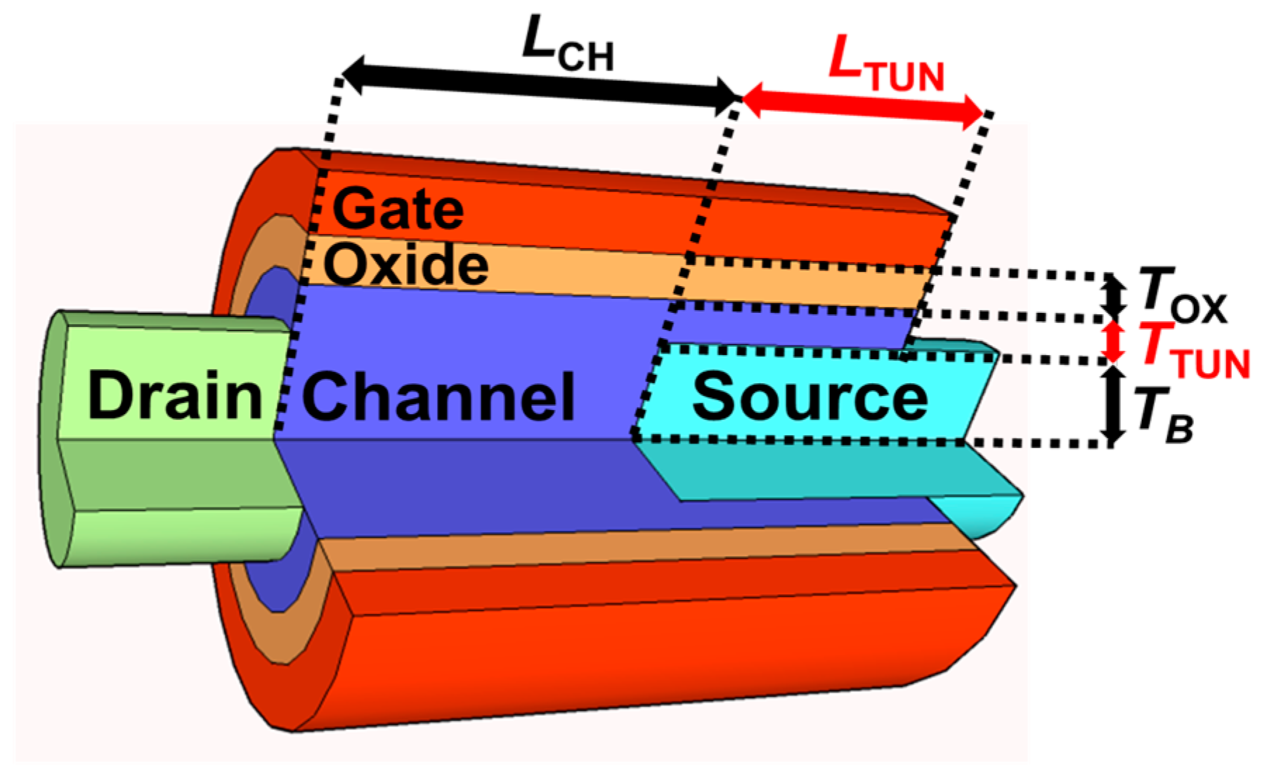
2. Device Fabrication
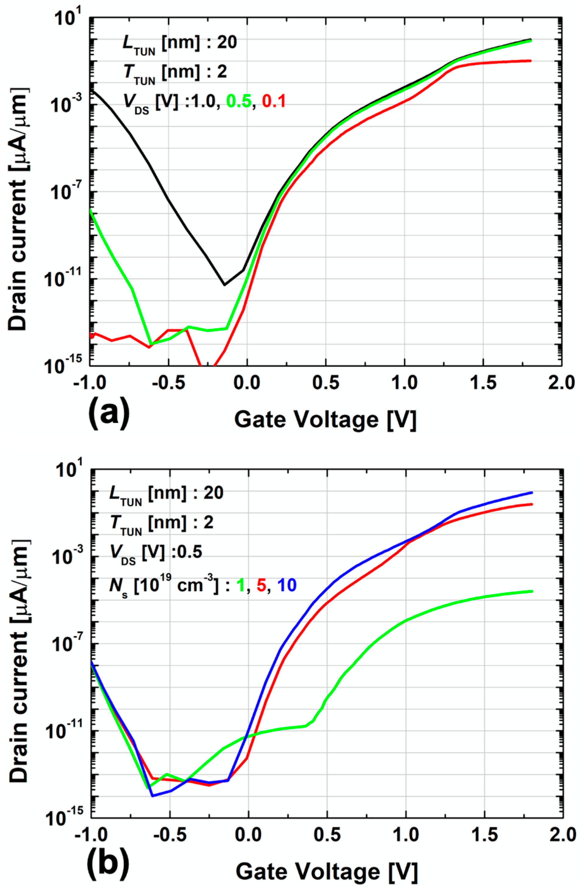
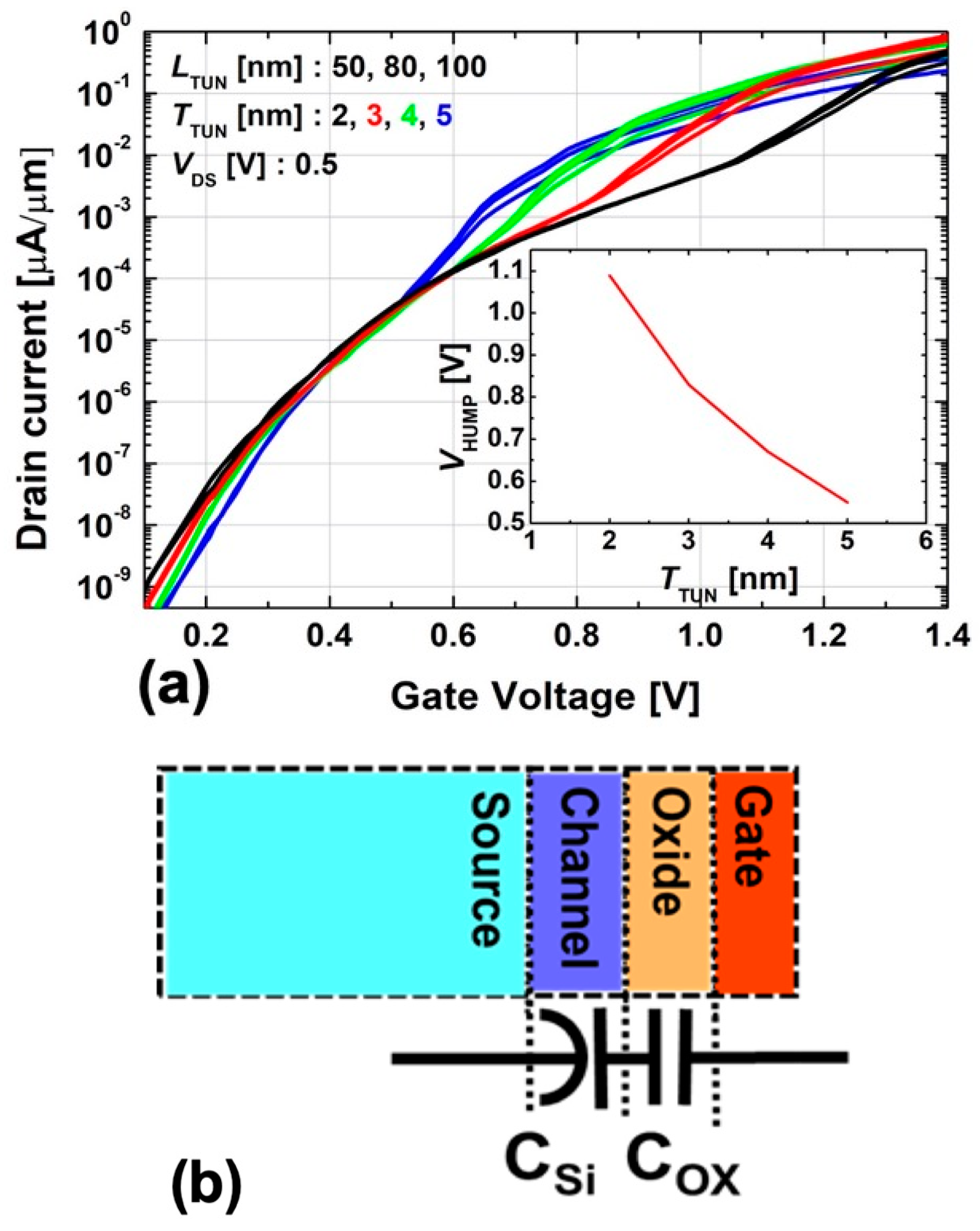
3. Hump Effect in SCNW TFET
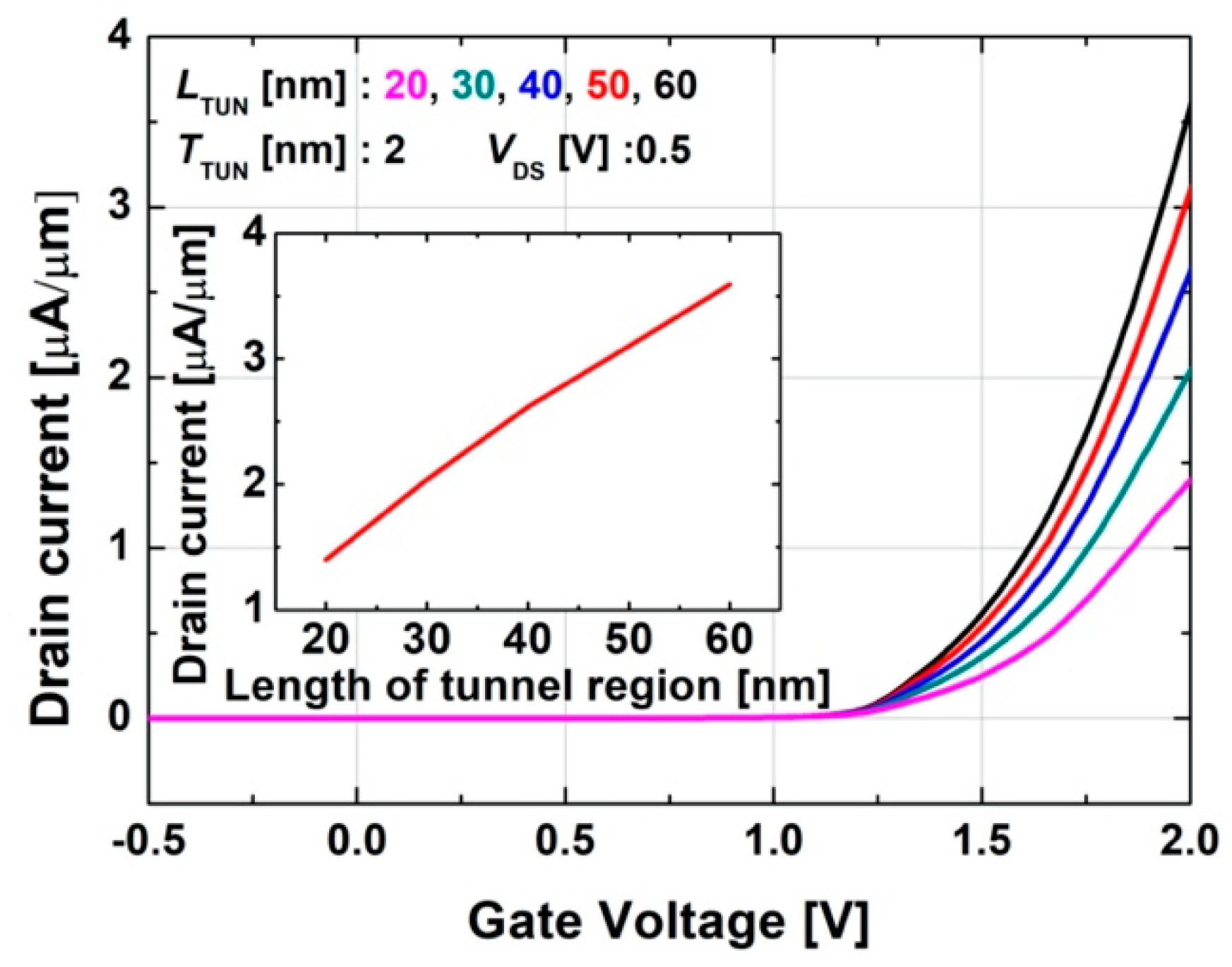
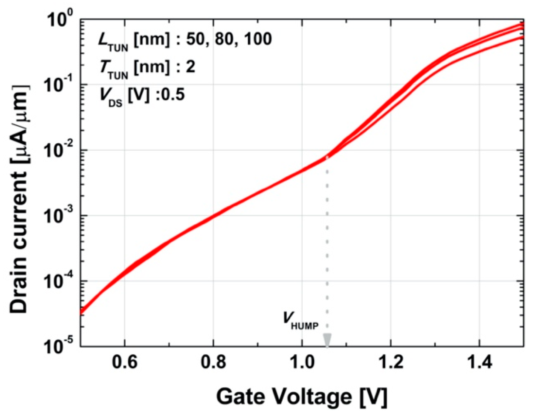
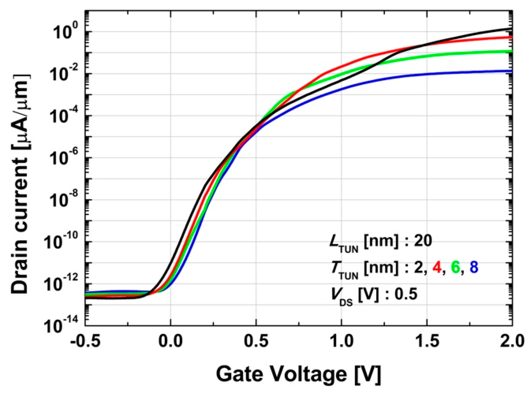
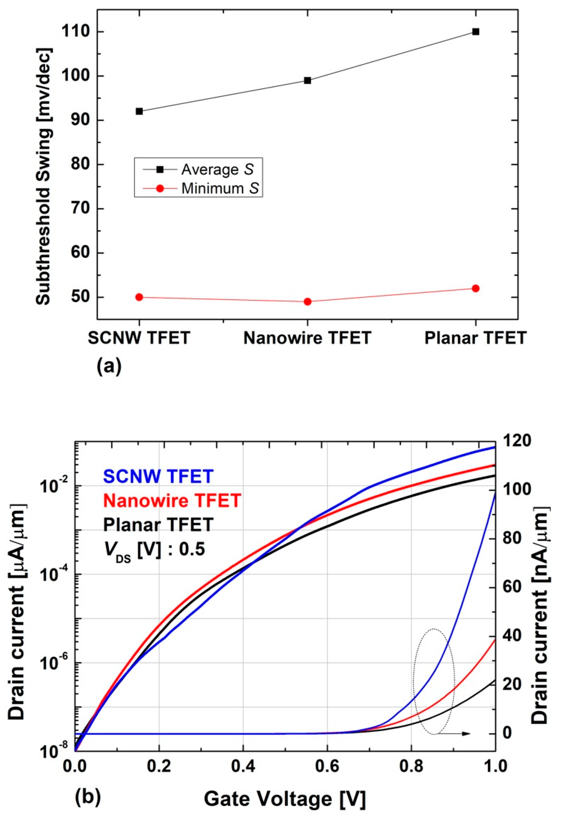
4. Device Optimization
5. Conclusions
Author Contributions
Funding
Conflicts of Interest
References
- Sakurai, T. Perspectives of low-power VLSI’s. IEICE Trans. Electron. 2004, E87-C, 429–436. [Google Scholar]
- Seabaugh, A.C.; Zhang, Q. Low-voltage tunnel transistors for beyond CMOS logic. Proc. IEEE 2010, 98, 2095–2110. [Google Scholar] [CrossRef]
- Choi, W.Y.; Park, B.G.; Lee, J.D.; Liu, T.J.K. Tunneling field-effect transistors (TFETs) with subthreshold swing (SS) less than 60 mV/dec. IEEE Electron Device Lett. 2007, 28, 743–745. [Google Scholar] [CrossRef]
- Bernstein, K.; Cavin, R.K.; Porod, W.; Seabaugh, A.; Welser, J. Device and architecture outlook for beyond CMOS switches. Proc. IEEE 2010, 98, 2169–2184. [Google Scholar] [CrossRef]
- Lattanzio, L.; De Michielis, L.; Ionescu, A.M. Complementary germanium electron-hole bilayer tunnel FET for sub-0.5-V operation. IEEE Electron Device Lett. 2012, 33, 167–169. [Google Scholar] [CrossRef]
- Cheng, W.; Liang, R.; Xu, G.; Yu, G.; Zhang, S.; Yin, H.; Zhao, C.; Ren, T.L.; Xu, J. Fabrication and characterization of a novel Si line tunneling TFET with high drive current. IEEE J. Electron Devices Soc. 2020, 8, 336–340. [Google Scholar] [CrossRef]
- Seabaugh, A. The tunneling transistor. IEEE Spectr. 2013, 50, 34–62. [Google Scholar] [CrossRef]
- Joshi, T.; Singh, B.; Singh, Y. Controlling the ambipolar current in ultrathin SOI tunnel FETs using the back-bias effect. J. Comput. Electron. 2020. [Google Scholar] [CrossRef]
- Sung, H.K.; Kam, H.; Hu, C.; Liu, T.J.K. Germanium-source tunnel field effect transistors with record high I ON/IOFF. In Proceedings of the Digest of Technical Papers—Symposium on VLSI Technology, Honolulu, HI, USA, 15–17 June 2009; pp. 178–179. [Google Scholar]
- Mayer, F.; Le Royer, C.; Damlencourt, J.F.; Romanjek, K.; Andrieu, F.; Tabone, C.; Previtali, B.; Deleonibus, S. Impact of SOI, Si1-xGexOI and GeOI Substrates on CMOS Compatible Tunnel FET performance. In Proceedings of the 2008 IEEE International Electron Devices Meeting, San Francisco, CA, USA, 15–17 December 2008; ISBN 9781424423781. [Google Scholar]
- Villalon, A.; Le Royer, C.; Nguyen, P.; Barraud, S.; Glowacki, F.; Revelant, A.; Selmi, L.; Cristoloveanu, S.; Tosti, L.; Vizioz, C.; et al. First demonstration of strained SiGe nanowires TFETs with ION beyond 700μA/μm. In Proceedings of the Digest of Technical Papers—Symposium on VLSI Technology, Honolulu, HI, USA, 9–12 June 2014; pp. 1–2. [Google Scholar]
- Ionescu, A.M.; Riel, H. Tunnel field-effect transistors as energy-efficient electronic switches. Nature 2011, 479, 329–337. [Google Scholar] [CrossRef]
- Kim, S.W.; Kim, J.H.; Liu, T.J.K.; Choi, W.Y.; Park, B.G. Demonstration of L-Shaped Tunnel Field-Effect Transistors. IEEE Trans. Electron Devices 2016, 63, 1774–1778. [Google Scholar] [CrossRef]
- Toh, E.H.; Wang, G.H.; Samudra, G.; Yeo, Y.C. Device physics and design of double-gate tunneling field-effect transistor by silicon film thickness optimization. Appl. Phys. Lett. 2007, 90, 263507. [Google Scholar] [CrossRef]
- Verhulst, A.S.; Vandenberghe, W.G.; Maex, K.; Groeseneken, G. Tunnel field-effect transistor without gate-drain overlap. Appl. Phys. Lett. 2007, 91, 53102. [Google Scholar] [CrossRef]
- Seo, J.H.; Yoon, Y.J.; Lee, S.; Lee, J.H.; Cho, S.; Kang, I.M. Design and analysis of Si-based arch-shaped gate-all-around (GAA) tunneling field-effect transistor (TFET). Curr. Appl. Phys. 2015, 15, 208–212. [Google Scholar] [CrossRef]
- Kao, K.H.; Verhulst, A.S.; Vandenberghe, W.G.; Soree, B.; Groeseneken, G.; De Meyer, K. Direct and indirect band-to-band tunneling in germanium-based TFETs. IEEE Trans. Electron Devices 2012, 59, 292–301. [Google Scholar] [CrossRef]
- Kao, K.H.; Verhulst, A.S.; Vandenberghe, W.G.; Sorée, B.; Magnus, W.; Leonelli, D.; Groeseneken, G.; De Meyer, K. Optimization of gate-on-source-only tunnel FETs with counter-doped pockets. IEEE Trans. Electron Devices 2012, 59, 2070–2077. [Google Scholar] [CrossRef]
- Kao, K.H.; Verhulst, A.S.; Vandenberghe, W.G.; De Meyer, K. Counterdoped pocket thickness optimization of gate-on-source-only tunnel FETs. IEEE Trans. Electron Devices 2013, 60, 6–12. [Google Scholar] [CrossRef]
- Betti Beneventi, G.; Gnani, E.; Gnudi, A.; Reggiani, S.; Baccarani, G. Optimization of a pocketed dual-metal-gate TFET by means of TCAD simulations accounting for quantization-induced bandgap widening. IEEE Trans. Electron Devices 2015, 62, 44–51. [Google Scholar] [CrossRef]
- Asai, H.; Mori, T.; Matsukawa, T.; Hattori, J.; Endo, K.; Fukuda, K. Steep switching less than 15 mV dec-1 in silicon-on-insulator tunnel FETs by a trimmed-gate structure. Jpn. J. Appl. Phys. 2019, 58, SBBA16. [Google Scholar] [CrossRef]
- Ashita; Loan, S.A.; Rafat, M. A High-Performance Inverted-C Tunnel Junction FET with Source-Channel Overlap Pockets. IEEE Trans. Electron Devices 2018, 65, 763–768. [Google Scholar] [CrossRef]
- Devi, W.V.; Bhowmick, B.; Pukhrambam, P.D. Investigation of dual MOSCAP TFET with improved vertical tunneling and its near infra-red sensing application. Semicond. Sci. Technol. 2020. [Google Scholar] [CrossRef]
- Software, D.S. ATLAS User’ s Manual; Scientific Software Development GmbH: Santa Clara, CA, USA, 2010; Volume II. [Google Scholar]
- Shaker, A.; Maged, A.; Elshorbagy, A.; AbouElainain, A.; Elsabbagh, M. Source-all-around tunnel field-effect transistor (SAA-TFET): Proposal and design. Semicond. Sci. Technol. 2019, 35, 25007. [Google Scholar] [CrossRef]
- Kim, S.W.; Choi, W.Y. Hump Effects of Germanium/Silicon Heterojunction Tunnel Field-Effect Transistors. IEEE Trans. Electron Devices 2016, 63, 2583–2588. [Google Scholar] [CrossRef]
- Synopsys Inc. Sentaurus Device User Guide-v.K-2015.06; Synopsys Inc.: Mountain View, CA, USA, 2009. [Google Scholar]
- Knoch, J. Optimizing tunnel FET performance—Impact of device structure, transistor dimensions and choice of material. In Proceedings of the International Symposium on VLSI Technology, Systems, and Applications, Hsinchu, Taiwan, 27–29 April 2009; pp. 45–46. [Google Scholar]
- Alper, C.; Palestri, P.; Padilla, J.L.; Ionescu, A.M. The electron-hole bilayer TFET: Dimensionality effects and optimization. IEEE Trans. Electron Devices 2016, 63, 2603–2609. [Google Scholar] [CrossRef]
- Ko, E.; Lee, H.; Park, J.D.; Shin, C. Vertical tunnel FET: Design optimization with triple metal-gate Layers. IEEE Trans. Electron Devices 2016, 63, 5030–5035. [Google Scholar] [CrossRef]
- Singh, N.; Agarwal, A.; Bera, L.K.; Liow, T.Y.; Yang, R.; Rustagi, S.C.; Tung, C.H.; Kumar, R.; Lo, G.Q.; Balasubramanian, N.; et al. High-performance fully depleted silicon nanowire (diameter ≤ 5 nm) gate-all-around CMOS devices. IEEE Electron Device Lett. 2006, 27, 383–386. [Google Scholar] [CrossRef]
- Duffy, R.; Meaney, F.; Galluccio, E. Doping considerations for finfet, gate-all-around, and nanosheet based devices. ECS Trans. 2020, 97, 63–74. [Google Scholar] [CrossRef]
- Hazbun, R.; Hart, J.; Hickey, R.; Ghosh, A.; Fernando, N.; Zollner, S.; Adam, T.N.; Kolodzey, J. Silicon epitaxy using tetrasilane at low temperatures in ultra-high vacuum chemical vapor deposition. J. Cryst. Growth 2016, 444, 21–27. [Google Scholar] [CrossRef]
- Smets, Q.; Verhulst, A.S.; El Kazzi, S.; Gundlach, D.; Richter, C.A.; Mocuta, A.; Collaert, N.; Thean, A.V.Y.; Heyns, M.M. Calibration of the effective tunneling bandgap in GaAsSb/InGaAs for improved TFET performance prediction. IEEE Trans. Electron Devices 2016, 63, 4248–4254. [Google Scholar] [CrossRef]
- Verhulst, A.S.; Verreck, D.; Smets, Q.; Kao, K.H.; Van De Put, M.; Rooyackers, R.; Sorée, B.; Vandooren, A.; De Meyer, K.; Groeseneken, G.; et al. Perspective of tunnel-FET for future low-power technology nodes. In Proceedings of the Technical Digest—International Electron Devices Meeting, IEDM, San Francisco, CA, USA, 15–17 December 2014. [Google Scholar]
- Kranthi, N.K.; Shrivastava, M. ESD Behavior of Tunnel FET Devices. IEEE Trans. Electron Devices 2017, 64, 28–36. [Google Scholar] [CrossRef]
- Madan, J.; Chaujar, R. Interfacial charge analysis of heterogeneous gate dielectric-gate all around-tunnel FET for improved device reliability. IEEE Trans. Device Mater. Reliab. 2016, 16, 227–234. [Google Scholar] [CrossRef]
- Zhu, H.; Li, Q.; Yuan, H.; Baumgart, H.; Ioannou, D.E.; Richter, C.A. Self-aligned multi-channel silicon nanowire field-effect transistors. Solid-State Electron. 2012, 78, 92–96. [Google Scholar] [CrossRef]
- Kim, S.W.; Choi, W.Y.; Sun, M.C.; Kim, H.W.; Park, B.G. Design guideline of Si-based L-shaped tunneling field-effect transistors. Jpn. J. Appl. Phys. 2012, 51, 06FE09. [Google Scholar] [CrossRef]
- Gandhi, R.; Chen, Z.; Singh, N.; Banerjee, K.; Lee, S. Vertical Si-Nanowire n-type tunneling FETs with low subthreshold swing ≤ 50 mV/decade) at room temperature. IEEE Electron Device Lett. 2011, 32, 437–439. [Google Scholar] [CrossRef]


| Parameters | Value |
|---|---|
| Source doping concentration, p-type (NS) | 1020 cm−3 |
| Drain doping concentration, n-type (ND) | 1020 cm−3 |
| Body doping concentration, p-type (NCH) | 1017 cm−3 |
| Gate work function | 4.05 eV |
| Channel length (LCH) | 30 nm |
| Nanowire radius except tunnel region (TB) | 7 nm |
| Gate oxide thickness (TOX) | 1 nm |
| Length of tunnel region (LTUN) | Variable |
| Thickness of tunnel region (TTUN) | Variable |
| Drain voltage (VDS) | 0.5 V |
© 2020 by the authors. Licensee MDPI, Basel, Switzerland. This article is an open access article distributed under the terms and conditions of the Creative Commons Attribution (CC BY) license (http://creativecommons.org/licenses/by/4.0/).
Share and Cite
Lee, S.-H.; Park, J.-U.; Kim, G.; Jee, D.-W.; Kim, J.H.; Kim, S. Rigorous Study on Hump Phenomena in Surrounding Channel Nanowire (SCNW) Tunnel Field-Effect Transistor (TFET). Appl. Sci. 2020, 10, 3596. https://doi.org/10.3390/app10103596
Lee S-H, Park J-U, Kim G, Jee D-W, Kim JH, Kim S. Rigorous Study on Hump Phenomena in Surrounding Channel Nanowire (SCNW) Tunnel Field-Effect Transistor (TFET). Applied Sciences. 2020; 10(10):3596. https://doi.org/10.3390/app10103596
Chicago/Turabian StyleLee, Seung-Hyun, Jeong-Uk Park, Garam Kim, Dong-Woo Jee, Jang Hyun Kim, and Sangwan Kim. 2020. "Rigorous Study on Hump Phenomena in Surrounding Channel Nanowire (SCNW) Tunnel Field-Effect Transistor (TFET)" Applied Sciences 10, no. 10: 3596. https://doi.org/10.3390/app10103596
APA StyleLee, S.-H., Park, J.-U., Kim, G., Jee, D.-W., Kim, J. H., & Kim, S. (2020). Rigorous Study on Hump Phenomena in Surrounding Channel Nanowire (SCNW) Tunnel Field-Effect Transistor (TFET). Applied Sciences, 10(10), 3596. https://doi.org/10.3390/app10103596