Abstract
This paper presents a low-noise multi-path operational amplifier for high-precision sensors. A chopper stabilization technique is applied to the amplifier to remove offset and flicker noise. A ripple reduction loop (RRL) is designed to remove the ripple generated in the process of up-modulating the flicker noise and offset. To cancel the notch in the overall transfer function due to the RRL operation, a multi-path architecture using both a low-frequency path (LFP) and high-frequency path (HFP) is implemented. The low frequency path amplifier is implemented using the chopper technique and the RRL. In the high-frequency path amplifier, a class-AB output stage is implemented to improve the power efficiency. The transfer functions of the LFP and HFP induce a first-order frequency response in the system through nested Miller compensation. The low-noise multi-path amplifier was fabricated using a 0.18 µm 1P6M complementary metal-oxide-semiconductor (CMOS) process. The power consumption of the proposed low-noise operational amplifier is 0.174 mW with a 1.8 V supply and an active area of 1.18 mm2. The proposed low-noise amplifier has a unit gain bandwidth (UGBW) of 3.16 MHz, an input referred noise of 11.8 nV/√Hz, and a noise efficiency factor (NEF) of 4.46.
1. Introduction
With the development of smart devices for Internet of Things (IoT), various sensor applications are becoming increasingly necessary. Among them, micro-electro-mechanical system (MEMS) sensors are receiving particular attention due to their small size, high signal-to-noise ratio (SNR), and low cost [1,2,3,4]. Sensing diminutive signals with a small output current and small output voltage amplitude using MEMS sensors requires large amplification. Therefore, high gain, high input impedance, and low-noise operational amplification are essential for various sensor interfaces [5,6,7]. To reduce output noise, chopper stabilization or auto-zeroing techniques are typically used [8]. The auto-zeroing technique typically operates using two phases. The first phase stores flicker noise and offset in the auto-zero capacitor, and the next phase subtracts the stored flicker noise and offset from the input signal. Because of these two phases, the auto-zeroing technique performs discrete-time operation. In addition, auto-zeroing techniques cause switching noise as well as noise folding of high-frequency components due to sampling operations, thus chopper-stabilized architecture is preferred for low-power and low-noise continuous-time applications [9]. Chopper stabilization techniques modulate the offset and flicker noise with a chopper frequency (fchop), leaving only thermal noise in the base band. However, the offset and the flicker noise are up-modulated, and these up-modulated noise signals are referred to as ripple. To attenuate this ripple, the ripple reduction loop (RRL) was proposed [10]. RRL integrates the generated ripple voltage at the output node and feeds back the integrated ripple to the input stage negatively. However, there is a limit in bandwidth because the transfer function of the amplifier produces a notch at the chopper frequency.
The bandwidth is increased by using a multi-path structure—a combination of a low-frequency path (LFP) and a high-frequency path (HFP). The transfer functions of the LFP and HFP induce a first-order frequency response in the system (a first-order system) by applying nested Miller compensation [11]. In the HFP, a class-AB output stage is implemented to improve the power efficiency. The proposed low-noise multi-path operational amplifier was fabricated using a 0.18-µm 1P6M complementary metal-oxide-semiconductor (CMOS) process. The average current consumption is 96.7 µA and the active area is 1.18 mm2. The proposed low-noise multi-path amplifier has a unit gain bandwidth (UGBW) of 3.16 MHz, an input referred noise of 11.8 nV/√Hz, and a noise efficiency factor (NEF) of 4.46.
2. Circuit Implementation of the Proposed Operational Amplifier
2.1. Architecture of the Proposed Multi-Path Operational Amplifier
The basic schematic is shown in Figure 1. The proposed circuit consists of two main paths, the HFP and LFP. In Figure 1, the red line represents the HFP and the blue line represents the LFP. The LFP consists of four stages, and the HFP consists of two stages. The LFP applies chopper stabilization to decrease the offset and flicker noise, while ripple is suppressed by the RRL. Connect the output of A6 in the current adder opposite to the output of A2 to suppress the ripple. The HFP has a first-order frequency response with one dominant pole caused by Cm1 and the LFP has a second-order frequency response with two dominant poles caused by Cm1 and Ci1. Nested Miller compensation is applied to smoothly combine the two frequency responses.
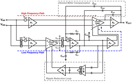
Figure 1.
Block diagram of the proposed chopper-stabilized multi-path operational amplifier with nested Miller compensation.
2.2. Low-Frequency Path Design
The LFP is shown in Figure 2. Because the LFP amplifies in four stages and the HFP in two stages, the LFP predominantly determines the offset and flicker noise of the overall amplifier. Using the chopper, the offset and flicker noise are up-modulated to the chopper frequency to reduce the offset and flicker noise in the baseband. The schematic of the input stage is shown in Figure 3. The common mode feedback (CMFB) of the current adder is implemented with an amplifier structure. The Vcmfb is set to 1/2 VDD so that the common mode voltage of the output Vop and Von are set to 1/2 VDD.
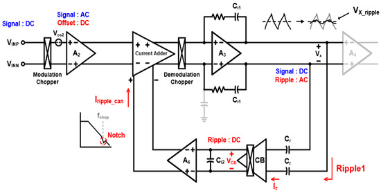
Figure 2.
Simplified implementation of the low-frequency path (LFP) with the ripple reduction loop (RRL).
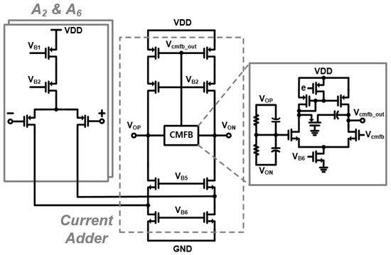
Figure 3.
Schematic of the input stage.
The signal is converted to a current through A2 and the ripple is converted to a current through A6. The two-signal current and the ripple current are subtracted through the current adder to suppress ripple. The output current of the current adder is converted to Vx through the A3 integrator. Vx is converted to a current through A4 and is merged with the HFP current through the current adder before A5.
2.3. Ripple Reduction Loop Design
The offset of A2 is shown in Vx as the ripple due to the demodulation chopper and integrator A3. When the transconductance of A2 is Gm2 and the frequency of the chopper is fch, the ripple at the output of A3 can be expressed as
When the transconductance of A4 is Gm4, this ripple is integrated again by integrator A5 so the ripple of the operational amplifier output can be expressed as
To reduce this ripple, the ripple reduction loop is used. The AC component Vripple1 is converted to the current Ir by the AC coupling capacitor Cr and is input into the current buffer (CB).
The CB is shown in Figure 4. If the output impedance of current source M1, M2, M7, and M8 is large enough, the output voltage and DC output impedance of the CB are given in Equations (4) and (5). The ACB is the DC voltage gain of the NMOS cascode in the CB. The output of the CB through A6 is combined to estimate the amount of ripple suppressed by the current adder, as given by Equation (6).
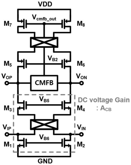
Figure 4.
Schematic of the current buffer (CB).
The simulation results of the ripple for Vx when a 10-mV offset exists are shown in Figure 5. The red line is the output waveform of Vx in Figure 2 when RRL is not working, and the blue line is the output waveform of Vx when RRL is operating. The ripple voltage was reduced by approximately 88%, from 68 mV to 8 mV by the RRL.
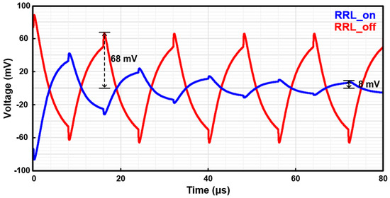
Figure 5.
Simulation results of the ripple reduction loop.
Finally, the ripple suppression factor F can be expressed as
2.4. High-Frequency Path Design
The HFP of the proposed operational amplifier is shown in Figure 6. The HFP consists of a folded cascode and a Monticelli-class AB output circuit [12] to increase power efficiency. The HFP becomes active when the loop gain of the HFP exceeds the loop gain of the LFP.
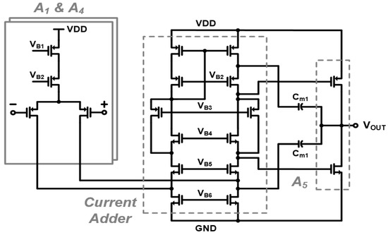
Figure 6.
Schematic of the high-frequency path (HFP).
2.5. Frequency Response
The LFP and HFP signals are combined by the current adder in Figure 6. The LFP has a second-order frequency response caused by A3 and A5 and the HFP has a first-order frequency response caused by A5. To smoothly merge the transfer functions of the two paths, the frequency response of the LFP must be made similar to that of a first-order system. To accomplish this, the poles were split by applying the nested Miller compensation to Cm1, Cm2, and Cm3. In the case of Cm2, as there is positive feedback, there is a risk that the operation of the entire amplifier will become unstable by inducing the pole to appear in the right half of the complex-s plane [13]. Therefore, Cm2 is connected to a negative terminal and its signal is implemented in the form of negative feedback.
The simulation results of the complete transfer function of the proposed operational amplifier are shown in Figure 7. The red line represents the HFP, the blue line represents the LFP, and the black line represents the overall transfer function of the multi-path operational amplifier. The frequency where the loop gain of the LFP and the loop gain of the HFP are equal is called the cross-over frequency and is determined by Ci1 and A4 in Figure 1. The overall transfer function follows the LFP function at low frequencies and the HFP function at high frequencies, and thus is not affected by the notch of the chopper frequency in the RRL. When the transconductance of A2 is Gm1, the frequency response of the proposed multi-path operational amplifier is seen as the first-order frequency response, so unit gain bandwidth (UGBW) can be expressed as Equation (8). The simulation results show that the UGBW of the proposed multi-path operational amplifier is 2.2 MHz.
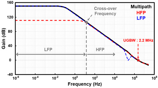
Figure 7.
Simulation results of the proposed operational amplifier transfer function.
2.6. Residual Input Offset
In the case of LFP, the offset and 1/f noise were suppressed using the chopper and RRL. Depending on the ripple suppression factor F, the residual ripple can ideally be removed completely. In the case of HFP, since there is no chopper that suppresses the offset, the input offset is shown as the residual input offset. In terms of residual input offset, the offset Vos1 of A1 can be expressed as Equation (9) when the gain of HFP is AHFP and the gain of LFP is ALFP [14].
The offset Vos3 of A3 also affects the residual input offset. Vos3 is represented by a square wave by chopper ch2 and parasitic capacitor Cp3_1-3. The current to charge and discharge Cp3_1-3 requires an input AC voltage of A2 [14]. This AC voltage becomes the DC voltage via chopper ch1 and appears as the residual input offset, which can be expressed as
Chopper ch2 consists of 4 CMOS switches, as shown in Figure 8. Switching errors occur due to clock feedthrough caused by a mismatch of parasitic capacitors Cp_ch21 and Cp_ch23 in chopper ch2, which is seen as input offset [14]. Cp_ch21 and the Cp_ch23 are parasitic capacitors generated between the input of chopper ch2 and the switch gate. Vclk is the voltage of the clock signal. The residual input offset can be expressed as
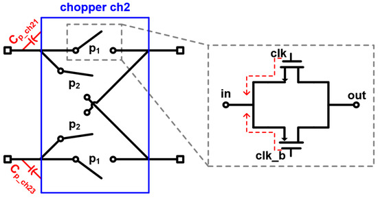
Figure 8.
Schematic of chopper ch2.
3. Measurement Results
3.1. Chip Die and Measurement Environment
The proposed multi-path operational amplifier was fabricated using a standard 0.18-µm CMOS process. Figure 9 shows the die photograph and measurement environment of the proposed operational amplifier. The power consumption of the proposed low-noise operational amplifier is 0.174 mW with a 1.8-V supply and an active area of 1.18 mm2. The fabricated chip was connected to a printed circuit board for circuit performance measurements. A waveform generator provided clock and other input signals, and signal acquisition and data analysis were performed using a digital oscilloscope. A dynamic signal analyzer was used to analyze the spectrum.
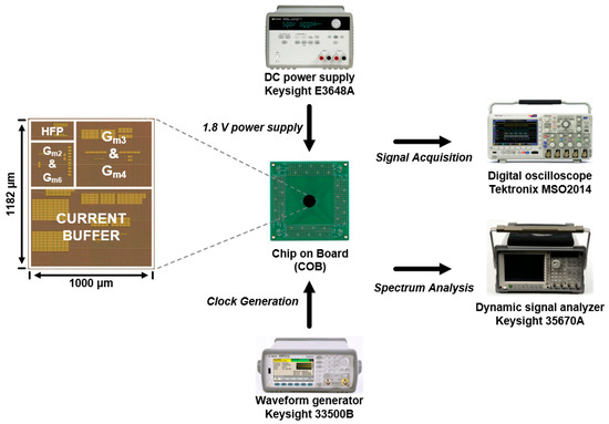
Figure 9.
Die photograph and measurement environment of the proposed operational amplifier.
3.2. Measurement Results
The sine wave input and output and pulse wave input and output results for the buffer operation of the proposed multi-path operational amplifier are shown in Figure 10. The x-axis of (a) is 400-µs scale, the y-axis is 200-mV scale, and the x-axis of (b) is 2-µs scale, the y-axis is 50-mV scale. The red wave is the input and the blue wave is the output of the amplifier. Sinusoidal and pulse waves with an amplitude of 100 mV were applied using a 50-pF capacitive load. For the pulse response, the rise time was 1.15 µs.
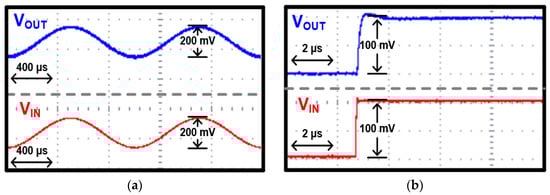
Figure 10.
Measurement results of the buffer operation: (a) input sine wave and (b) input pulse wave.
The slew rate measurement results are shown in Figure 11. The red wave is the input and the blue wave is the output of the amplifier. The proposed multi-path operational amplifier exhibits a slew rate of 0.86 V/µs when a 1 V amplitude pulse wave is applied.
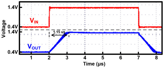
Figure 11.
Measurement results of the slew rate.
Figure 12 shows the open loop gain measurement result of the proposed multi-path operational amplifier. The proposed operational amplifier has a gain of 135 dB at 1 Hz and exhibits a first-order frequency response. The proposed operational amplifier has a gain of 50 dB at 10 kHz and a unit gain bandwidth (UGBW) of 3.16 MHz. Compared with the simulation results in Figure 7, similar values are measured.
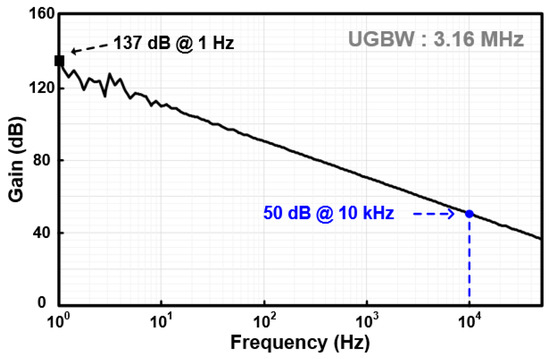
Figure 12.
Open loop gain measurement results of the proposed multi-path operational amplifier.
Figure 13 shows the common mode rejection ratio (CMRR) and power supply rejection ratio (PSRR) measurements of the proposed multi-path operational amplifier. The proposed operational amplifier has a CMRR of 125 dB at 1 Hz and a PSRR of 100 dB at 1 Hz. The minimum values of the CMRR and PSRR are 69.8 dB and 71.7 dB.
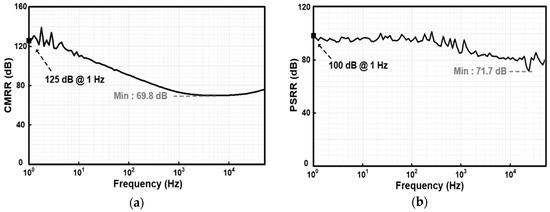
Figure 13.
Measurement results: (a) the common mode rejection ratio (CMRR); (b) power supply rejection ratio (PSRR).
Figure 14 shows the results of the input referred offset measurement of the proposed multi-path amplifier. The input referred offset measurement shows that the average input offset is 1.99 µV and peak-to-peak offset is 3.73 µV.
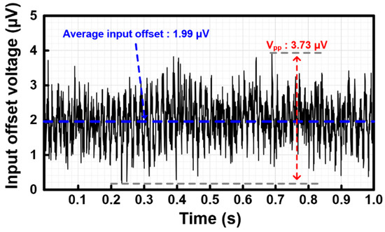
Figure 14.
Input referred offset measurement result of the proposed multi-path amplifier.
The noise measurement results of the proposed multi-path operational amplifier for a bandwidth of 0.5–200 Hz are shown in Figure 15. Figure 15a shows the input referred noise of the proposed operational amplifier. The measured input referred noise is 47.8 nV/√Hz at 1 Hz and 10.8 nV/√Hz at 200 Hz. Figure 15b shows a noise histogram at 200 Hz for 10 samples. The average value of the input referred noise at 200 Hz for the 10 samples is 11.8 nV/√Hz.
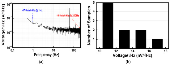
Figure 15.
Noise measurement results of the proposed multi-path amplifier: (a) input referred noise and (b) histogram of the measured input referred noise at 200 Hz.
4. Discussion
A performance comparison with previous low-noise amplifier studies is shown in Table 1. When Vni is the input referred noise and Itot is the total consumption current of the operational amplifier, the NEF of the performance comparison can be obtained from Equation (15) [15]. The proposed low-noise chopper-stabilized multi-path operational amplifier achieves a current consumption of 96.7 µA with a 1.8 V power supply, UGBW of 3.16 MHz, and input referred noise of 11.8 nV/√Hz, resulting in a NEF of 4.46.

Table 1.
Performance comparison: summary of measured parameters.
Because of the multi-path architecture, the proposed multi-path operational amplifier is relatively large in size and power consumption, but has a low input referred noise and wide bandwidth, so its NEF is better than previous studies.
5. Conclusions
This paper has presented a low-noise chopper-stabilized multi-path operational amplifier with nested Miller compensation for high-precision sensors. The proposed multi-path operational amplifier removes the offset, flicker noise, and ripple by applying a chopper stabilization technique and RRL, and enables wide bandwidth operation using a multi-path structure. Nested Miller compensation is applied to obtain the frequency response of a clean first-order system. The proposed multi-path operational amplifier was fabricated using a standard 0.18-µm CMOS process and an active area of 1.18 mm2. The power consumption is 0.174 mW with a 1.8 V power supply. It achieves a slew rate of 0.86 V/ µs, >137 dB open loop gain, >125 dB CMRR, and >100 dB PSRR. The NEF of 4.46 was obtained based on the achieved input referred noise of 11.8 nV/√Hz and UGBW of 3.16 MHz. The proposed low-noise multi-path operational amplifier has a good NEF and is suitable for precision sensor applications.
Author Contributions
H.K. (Hyoungho Ko) conceived the study; H.K. (Hyungseup Kim), K.H., D.Y., H.H., Y.K., and D.C. designed the experiments; all authors participated in the tests and evaluations; J.K. wrote the paper. All authors have read and agreed to the published version of the manuscript.
Funding
This research was supported by the Practical technology development medical microrobot Program (R&D Center for Practical Medical Microrobot Platform. HI19C0642) funded by the Ministry of Health and Welfare (MOHW, Korea) and Korea Health Industry DEVELOPMENT Institute (KHIDI, Korea).
Acknowledgments
Chip fabrication and the EDA tool were supported by the IC Design Education Center (IDEC), Republic of Korea.
Conflicts of Interest
The authors declare no conflicts of interest.
References
- Sun, H.; Fang, D.; Jia, K.; Maarouf, F.; Qu, H.; Xie, H. A low-power low-noise dual-chopper amplifier for capacitive CMOS-MEMS accelerometers. IEEE Sens. J. 2010, 11, 925–933. [Google Scholar] [CrossRef]
- Tan, Z.; Shalmany, S.H.; Meijer, G.C.; Pertijs, M.A. An energy-efficient 15-bit capacitive-sensor interface based on period modulation. IEEE J. Solid State Circuits 2012, 47, 1703–1711. [Google Scholar] [CrossRef]
- Yu, H.Y.; Qin, M.; Huang, J.Q.; Huang, Q.A. A MEMS capacitive pressure sensor compatible with CMOS process. In Proceedings of the SENSORS 2012 IEEE, Taipei, Taiwan, 28–31 October 2012; IEEE: Piscataway, NJ, USA, 2012; pp. 1–4. [Google Scholar]
- Ladani, L.; Nelson, S. A novel piezo-actuator-sensor micromachine for mechanical characterization of micro-specimens. Micromachines 2010, 1, 129–152. [Google Scholar] [CrossRef]
- Belloni, M.; Bonizzoni, E.; Fornasari, A.; Maloberti, F. A micropower chopper—CDS operational amplifier. IEEE J. Solid State Circuits 2010, 45, 2521–2529. [Google Scholar] [CrossRef]
- Kim, H.; Song, H.; Park, Y.; Ko, H. Low noise resistive analog front-end with automatic offset calibration loop. In Proceedings of the 2015 International SoC Design Conference (ISOCC), Gyungju, Korea, 2–5 November 2015. [Google Scholar]
- Wu, R.; Huijsing, J.H.; Makinwa, K.A. A 21b ± 40 mV range read-out IC for bridge transducers. In Proceedings of the 2011 IEEE International Solid-State Circuits Conference, San Francisco, CA, USA, 20–24 February 2011. [Google Scholar]
- Enz, C.C.; Temes, G.C. Circuit techniques for reducing the effects of op-amp imperfections: Autozeroing, correlated double sampling, and chopper stabilization. Proc. IEEE 1996, 84, 1584–1614. [Google Scholar] [CrossRef]
- Ko, Y.; Kim, H.; Park, Y.; Mun, Y.; Cho, D.I.D.; Ko, H. Low-Noise Chopper-Stabilized Resistive Readout Integrated Circuit with Ripple Rejection Loop. Sens. Mater. 2017, 29, 927–933. [Google Scholar]
- Wu, R.; Makinwa, K.A.; Huijsing, J.H. A chopper current-feedback instrumentation amplifier with a 1 mHz 1/f noise corner and an AC-coupled ripple reduction loop. IEEE J. Solid State Circuits 2009, 44, 3232–3243. [Google Scholar] [CrossRef]
- Eschauzier, R.G.; Kerklaan, L.P.; Huijsing, J.H. A 100-MHz 100-dB operational amplifier with multipath nested Miller compensation structure. IEEE J. Solid-State Circuits 1992, 27, 1709–1717. [Google Scholar] [CrossRef]
- Monticelli, D.M. A Quad CMOS Single-Supply Op Amp with Rail-to-Rail Output Swing. IEEE J. Solid-State Circuits 1986, 21, 1026–1034. [Google Scholar] [CrossRef]
- Eschauzier, R.G.; Hogervorst, R.; Huijsing, J.H. A programmable 1.5 V CMOS class-AB operational amplifier with hybrid nested Miller compensation for 120 dB gain and 6 MHz UGF. IEEE J. Solid State Circuits 1994, 29, 1497–1504. [Google Scholar] [CrossRef]
- Witte, F.; Huijsing, J.H.; Makinwa, K.A. Dynamic Offset Compensated CMOS Amplifiers; Springer: Berlin, Germany, 2010; pp. 23–40. [Google Scholar]
- Steyaert, M.S.J.; Sansen, W.M.C. A Micropower Low-Noise Monolitic Instrumentation 284 Amplifier for Medical Purposes. IEEE J. Solid-State Circuits 1987, 22, 1163–1168. [Google Scholar] [CrossRef]
- Fan, Q.; Huijsing, J.H.; Makinwa, K.A. A 21 nV/√Hz Chopper-Stabilized Multi-Path Current-Feedback Instrumentation Amplifier with 2 µV Offset. IEEE J. Solid State Circuits 2011, 47, 464–475. [Google Scholar]
- Burt, R.; Zhang, J. A micropower chopper-stabilized operational amplifier using a SC notch filter with synchronous integration inside the continuous time signal path. In Proceedings of the 2006 IEEE International Solid-State Circuits Conference-Digest of Technical Papers, San Francisco, CA, USA, 6–9 February 2006. [Google Scholar]
- Kusuda, Y. A 5.9 nV/√ Hz chopper operational amplifier with 0.78 μV maximum offset and 28.3 nV/°C offset drift. In Proceedings of the 2011 IEEE International Solid-State Circuits Conference, San Francisco, CA, USA, 20–24 February 2011. [Google Scholar]
- Ong, G.T.; Chan, P.K. A power-aware chopper-stabilized instrumentation amplifier for resistive wheatstone bridge sensors. IEEE Trans. Instrum. Meas. 2014, 63, 2253–2263. [Google Scholar] [CrossRef]
- Lue, D.; Zhang, M.; Wang, Z. A Low-Noise Chopper Amplifier Designed for Multi-Channel Neural Signal Acquisition. IEEE J. Solid State Circuits 2019, 54, 2255–2265. [Google Scholar] [CrossRef]
- Butti, F.; Piotto, M.; Bruschi, P. A Chopper Instrumentation Amplifier with Input Resistance Boosting by Means of Synchronous Dynamic Element Matching. IEEE Trans. Circuits Syst. I Regul. Pap. 2017, 64, 753–794. [Google Scholar] [CrossRef]
© 2019 by the authors. Licensee MDPI, Basel, Switzerland. This article is an open access article distributed under the terms and conditions of the Creative Commons Attribution (CC BY) license (http://creativecommons.org/licenses/by/4.0/).