Article

Fully Differential Chopper-Stabilized Multipath Current-Feedback Instrumentation Amplifier with R-2R DAC Offset Adjustment for Resistive Bridge Sensors

1
Department of Electronics Engineering, Chungnam National University, Daejeon 34134, Korea
2
ASRI/ISRC, Department of Electrical and Computer Engineering, Seoul National University, Seoul 08826, Korea
*
Author to whom correspondence should be addressed.
Appl. Sci. 2020, 10(1), 63; https://doi.org/10.3390/app10010063
Submission received: 2 December 2019 / Revised: 17 December 2019 / Accepted: 18 December 2019 / Published: 20 December 2019
(This article belongs to the Special Issue Selected Papers from IMETI 2018)

Abstract

:
A fully differential multipath current-feedback instrumentation amplifier (CFIA) for a resistive bridge sensor readout integrated circuit (IC) is proposed. To reduce the CFIA’s own offset and 1/f noise, a chopper stabilization technique is implemented. To attenuate the output ripple caused by chopper up-modulation, a ripple reduction loop (RRL) is employed. A multipath architecture is implemented to compensate for the notch in the chopping frequency band of the transfer function. To prevent performance degradation resulting from external offset, a 12-bit R-2R digital-to-analog converter (DAC) is employed. The proposed CFIA has an adjustable gain of 16–44 dB with 5-bit programmable resistors. The proposed resistive sensor readout IC is implemented in a 0.18 μm complementary metal-oxide-semiconductor (CMOS) process. The CFIA draws 169 μA currents from a 3.3 V supply. The simulated input-referred noise and noise efficiency factor (NEF) are 28.3 nV/√Hz and 14.2, respectively. The simulated common-mode rejection ratio (CMRR) is 162 dB, and the power supply rejection ratio (PSRR) is 112 dB.

1. Introduction

Recently, the Internet of Things (IoT) has played a significant role in many aspects of modern life, such as medical care, automobiles, homes, and amenities [1]. IoT sensors that perceive and collect information and circuits that readout these sensors with high precision are also becoming more important [2]. Resistive micro-electro-mechanical systems (MEMS) sensors that use a piezoresistive effect have various ways, such as strain gauges and pressure, acceleration, and force sensors [3,4,5,6,7]. The need for smaller, less expensive high-performance sensors has developed in a way that makes sensors and sensing elements smaller. To readout these sensors precisely, readout circuits should have low-noise, high input impedance, low power, and high common-mode rejection ratio (CMRR) characteristics. Conventionally, the well-known 3-opamp instrumentation amplifier (IA) scheme features a high input impedance. Its disadvantage is that the degree of matching resistance greatly influences the CMRR, making it difficult to achieve a high CMRR. A current-feedback instrumentation amplifier (CFIA) consists of an input transconductance stage and output Miller integrator stage. The CFIA scheme features high input impedance, high CMRR, high open-loop gain, and low power consumption, because the input common-mode (CM) voltage is isolated by the input transconductance stage [8]. Although the CFIA has advantages in terms of its simple structure, the input offset and noise can cause performance degradation. To implement the low-noise characteristics of the instrumentation amplifier (IA), auto-zeroing, correlated double sampling (CDS), and the chopper stabilization technique are the most widely used schemes [9,10,11,12]. Unlike thermal noise with a wide frequency band, flicker noise and DC offset overlap with the sensor output signal. For the desired output voltage of the IA, reduction of flicker noise and DC offset are essential. The auto-zeroing and CDS schemes sample the offsets in the input capacitor of the IA, which attenuates flicker noise and DC offset through comparison and amplification. However, the high-frequency thermal noise folds and appears in integrated form in the baseband because of aliasing. The chopper stabilization technique reduces baseband noise through up-modulating the flicker noise and DC offset in the baseband; thus, a thermal-noise-limited level can be achieved. However, up-modulated DC offset and flicker noise can cause a ripple in the output. To solve this problem, a ripple reduction loop (RRL) is used to demodulate the ripple and provide negative feedback to the input through the integrator [13]. The RRL attenuates the output ripple caused by chopping, but there are disadvantages to generating notches of the transfer function in the chopping frequency band.
In this study, a low-noise bridge resistive sensor readout circuit with dual offset reduction is implemented. (1) The offset inside the amplifier is reduced by the multipath offset stabilization topology. (2) The offset outside the amplifier is adjusted by the R-2R digital-to-analog converter (DAC) in the current-feedback path. To attenuate the flicker noise and DC offset in the baseband, the chopper stabilization technique is employed. The RRL is adopted to attenuate the output ripple. A multipath topology is employed to compensate for the notches of the transfer function in the chopping frequency band. This CFIA achieves a high CMRR, high input impedance, and low power consumption.

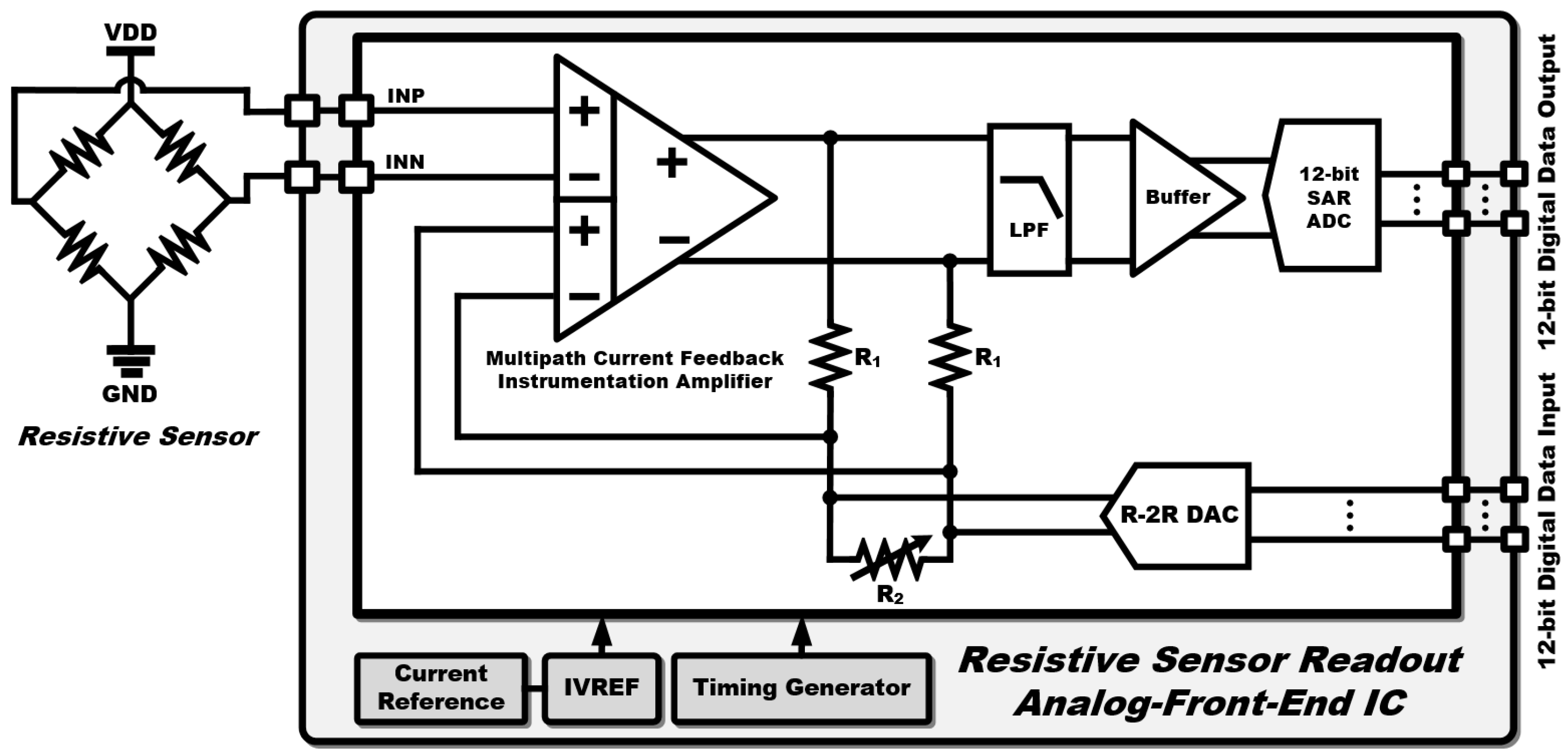
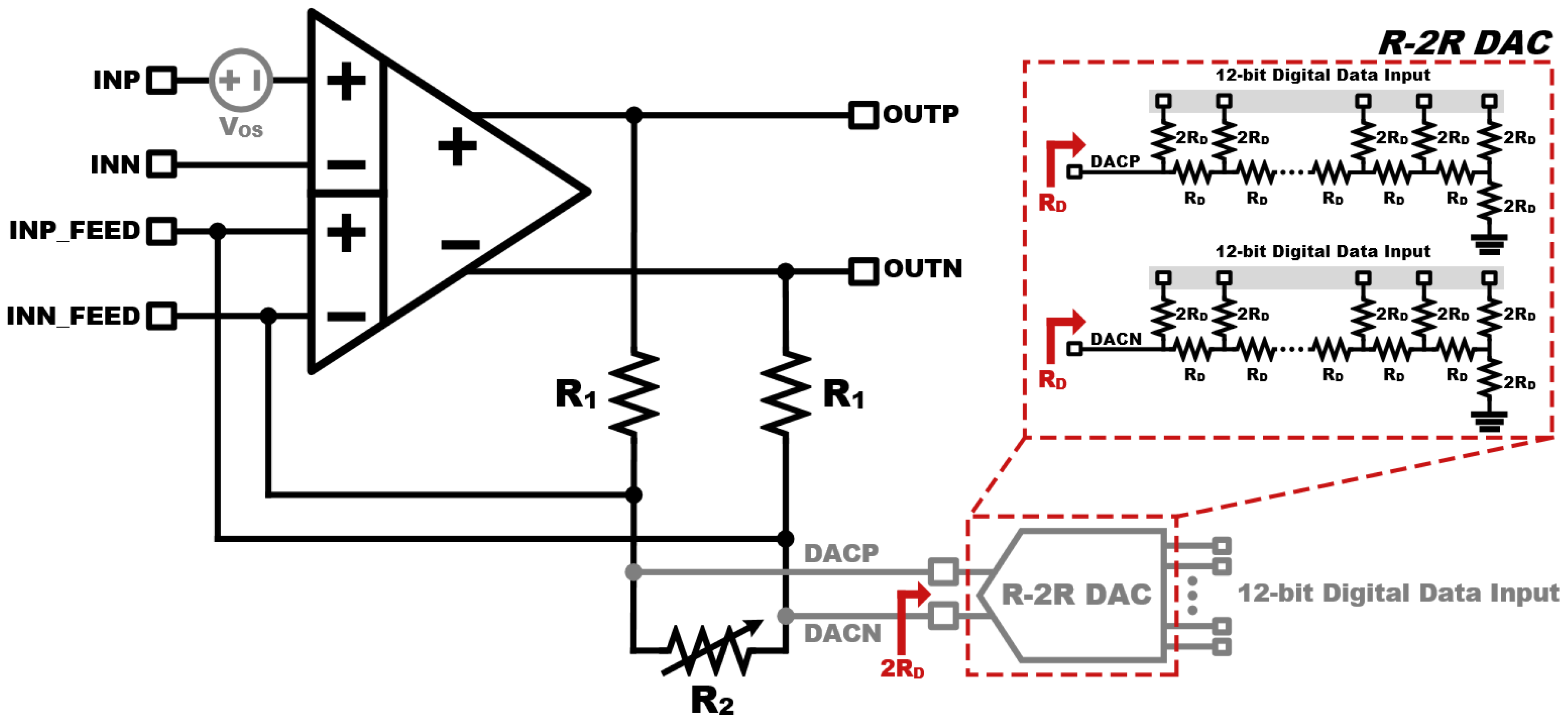
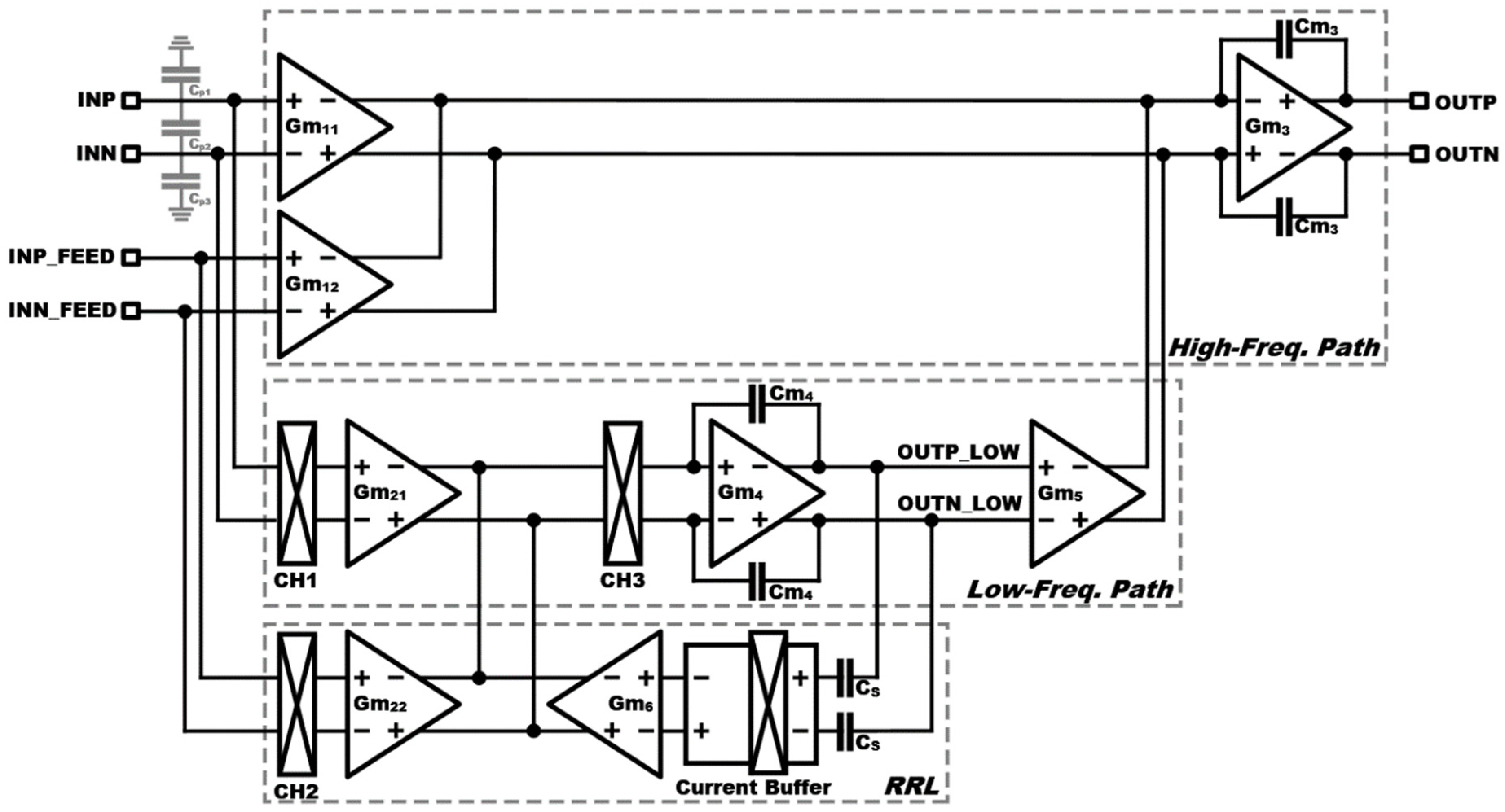
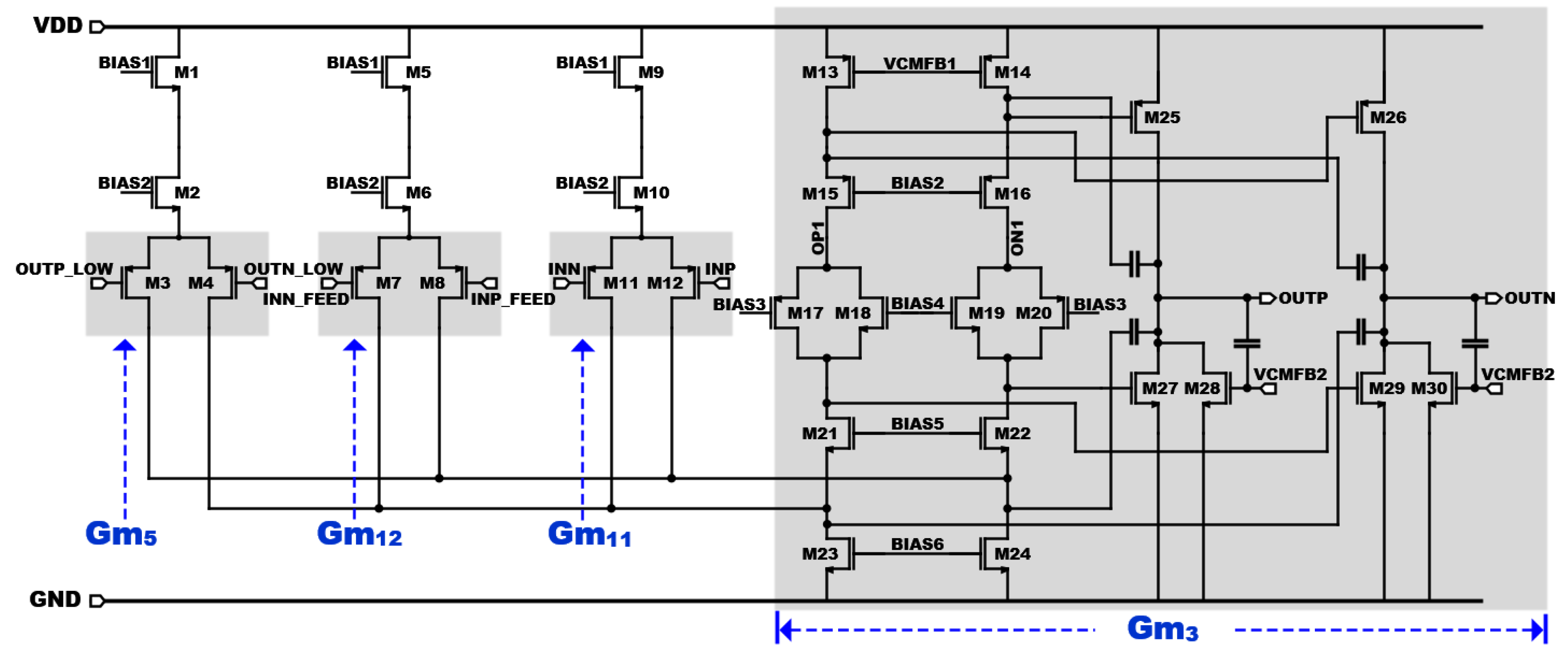
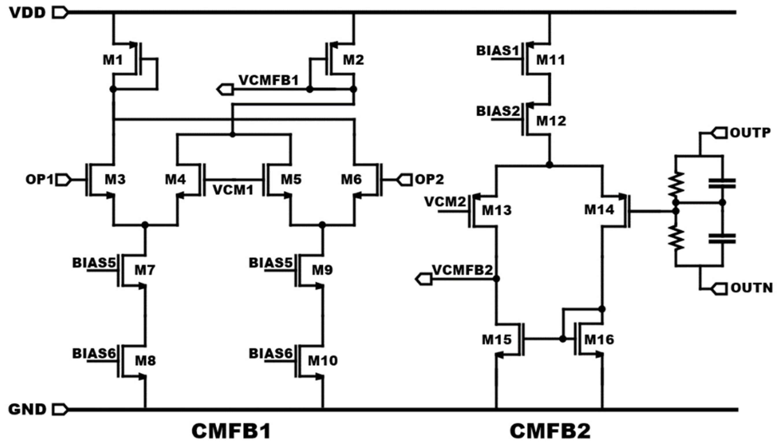
2. Circuit Implementation

Figure 1 shows the proposed resistive sensor readout analog-front-end (AFE) IC architecture. The architecture consists of a multipath CFIA, low-pass filter (LPF), buffer, 12-bit successive approximation register analog-to-digital converter (SAR ADC), R-2R DAC, and feedback resistor. To drive a variety of resistive sensors, the feedback resistor R2 is designed by implementing a 5-bit programmable resistor. Depending on the external 5-bit digital input, the proposed resistive sensor readout AFE has an adjustable gain of 16–44 dB. Figure 2 shows the operation of the R-2R DAC calibration. The R-2R DAC is designed to compensate for the external offset generated by sensor element mismatches. The R-2R DAC has the ability to adjust the amplified external offset voltage between 3.3 V and -3.3V, with 1.61 mV intervals through the 12-bit digital input. The output voltage of the proposed CFIA without the external offset and R-2R DAC is expressed as (1).
O U T P O U T N = ( 1 + 2   × R 1 R 2 ) × ( I N P I N N )
Each unit of the R-2R DAC, consisting of RD and 2RD resistors, has an output resistance of RD. The output resistance between the DACP and DACN node can be interpreted as 2RD. Therefore, the output voltage of the proposed CFIA with R-2R DAC is expressed as (2).
O U T P O U T N = ( 1 + 2   × R 1 R 2 ) × ( I N P I N N ) +   R 1 R D × ( ( I N P I N N ) ( D A C P D A C N ) )
Through the second term of (2), the amplified external offset can be calibrated. In this design, R1 can influence offset calibration. Therefore, R2, which is independent from offset calibration, is configured as a programmable resistor.
Figure 3 shows the block diagram of the proposed CFIA. The proposed fully differential CFIA circuit consists of two main signal paths: a low-frequency and a high-frequency path. The low-frequency path employs the chopper stabilization technique to reduce flicker noise and DC offset in the baseband. To reduce the ripple caused by chopping, the RRL is implemented. To compensate for the notch in the transfer function of the chopping frequency band, the high-frequency path is used.

2.1. Low-Frequency Path

The R-2R DAC reduces the offset caused by sensor element mismatches but does not reduce the IA’s own internal offset. The chopper implements an internal offset reduction. The chopper is operated by two nonoverlapping clocks. As shown in Figure 3, the sensor output signal is modulated into the high-frequency band through a modulation chopper (CH1), and the modulated signal is demodulated back into the baseband through the demodulation chopper (CH3). Simultaneously, a modulation chopper (CH3) modulates flicker noise and DC offset into the high-frequency band. Consequentially, the up-modulated flicker noise and DC offset are reduced through a Miller integrator (Gm4) and combined with high-frequency path signals. At the output of the Miller integrator (Gm4), the up-modulated flicker noise and DC offset generate a ripple. The ripple is negative feedback to the input of the chopper (CH3) through an AC coupling capacitor (Cs) and the current buffer.
The overall input impedance of the CFIA is determined by the switched capacitor resistor, and is generated by the chopping frequency and input parasitic capacitor (Cp1, Cp2, and Cp3). Consequently, the input impedance is inversely proportional to the chopping frequency and input parasitic capacitor. If the chopping frequency is reduced to increase the impedance, the output ripple increases. If the parasitic capacitor is reduced to increase the impedance, flicker noise tends to prevail. Achieving high-performance CFIA requires delicate consideration of trade-offs between noise and input impedance.

2.2. High-Frequency Path

Figure 4 shows a schematic of the high-frequency path. The high-frequency path consists of a three-input transconductance stage and the Miller integrator. The input, feedback, and low-frequency path output signals are converted to currents through Gm11, Gm12, and Gm5, respectively, and entered into the Miller integrator. At the Gm3 stage, to achieve a fine-frequency response in the high-frequency path, nested Miller compensation is implemented [14]. To compensate for the drawbacks of the dead-band in the crossover area, a Monticelli class AB output stage is implemented (M17, M18, M19, and M20). It has the advantages of linear output characteristics and distortion reduction. Figure 5 shows a schematic of the high-frequency path common-mode feedback (CMFB) circuit. The gate voltage of transistors M13 and M14 is determined by the active CMFB circuit, which has the advantage of increasing bandwidth. To stabilize the output voltage, the CMFB circuit is also implemented at the output stage.

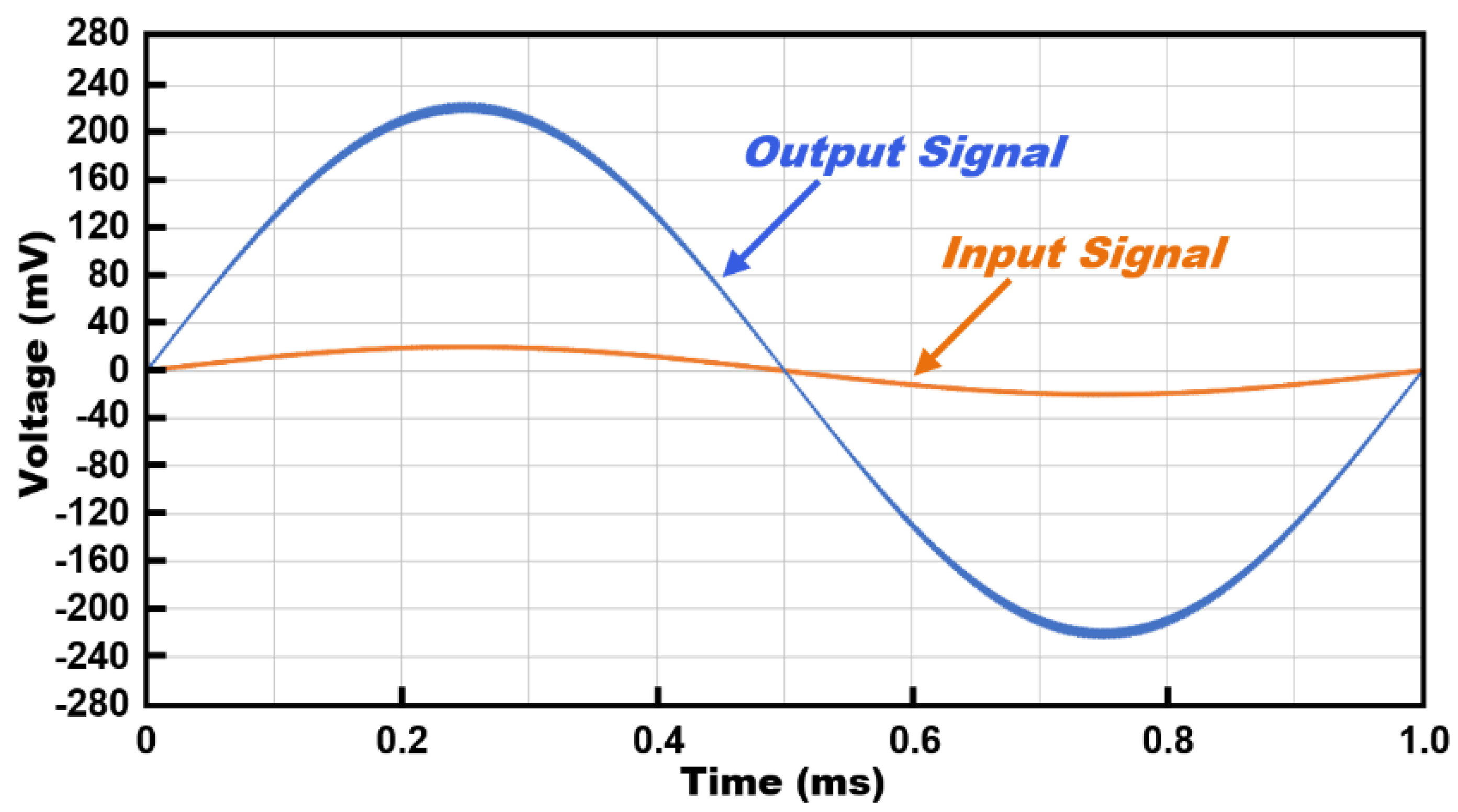
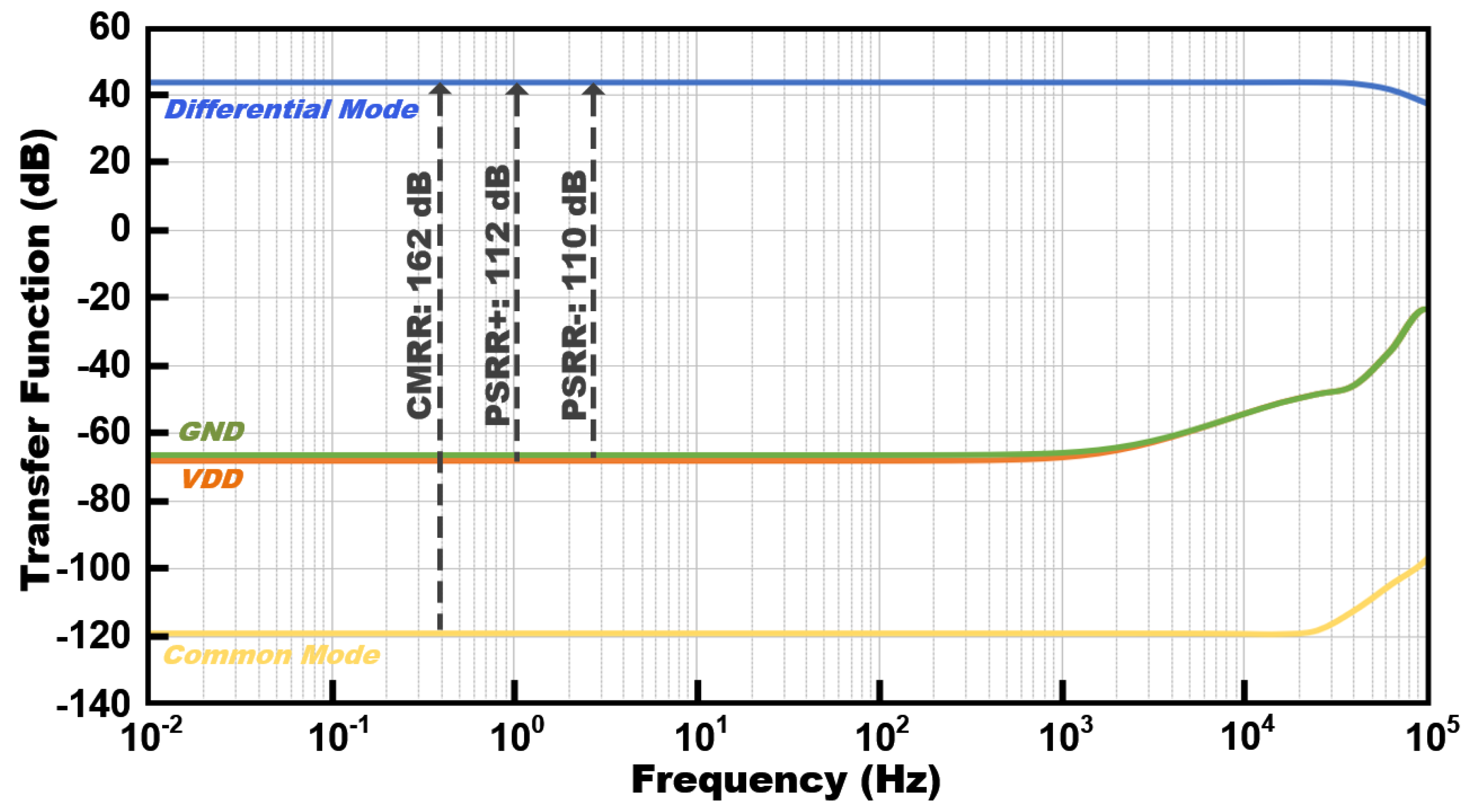
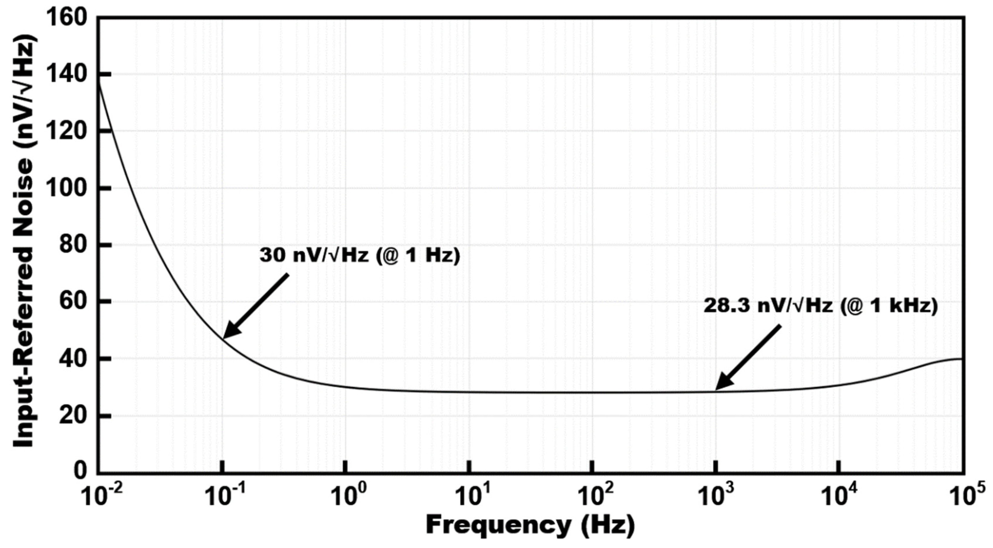
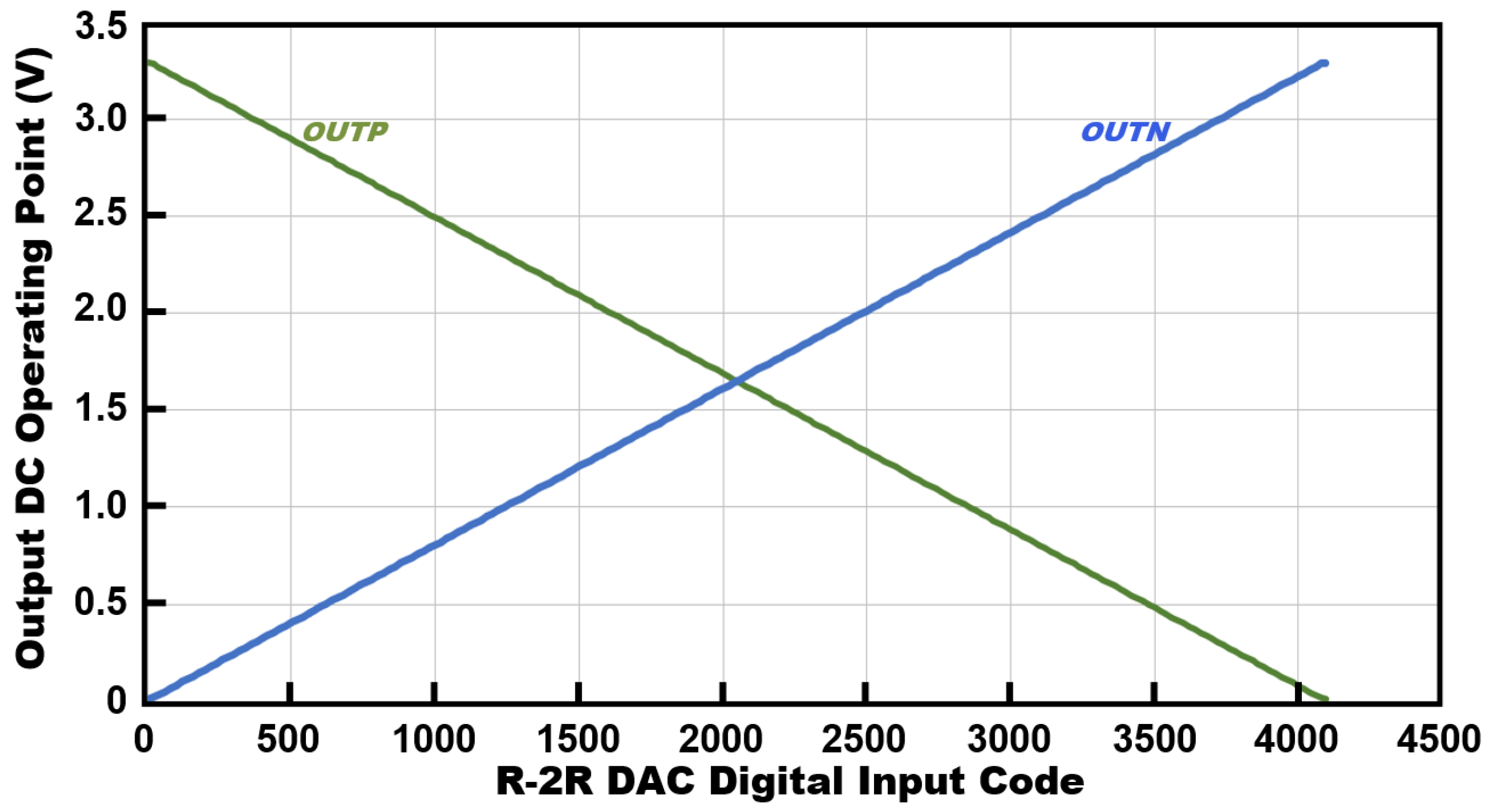
3. Simulation Results

Figure 6 shows the transient response of a CFIA with a 20mV amplitude input sine wave of 1 kHz. The gain of the CFIA was set to have 11 V/V through a 5-bit programmable resistor. The graph shows the input/output in the form of a differential signal. The output signal is simulated to have a peak value of 220.07 mV at 0.25 ms. Figure 7 shows the simulated transfer function in differential mode, VDD, GND, and common-mode. The simulated CMRR achieves 162 dB. The power supply rejection ratio (PSRR+ and PSRR-) are simulated at 112 and 110 dB, respectively. Figure 8 shows the frequency response of the CFIA. The open-loop gain is simulated at 132.5 dB at 1 mHz. The simulated unit gain bandwidth (UGBW) is 59.2 kHz, and the phase margin is 75.1° at UGBW. Figure 9 shows the simulated input-referred noise. The simulated input-referred noise is 30 nV/√Hz at 1 Hz and 28.3 nV/√Hz at 1 kHz.
Figure 10 shows the simulated CFIA output DC operating point under R-2R DAC digital input variation. It shows that the offset of the CFIA output can be linearly calibrated within a ±3.3 V range. The performance summary and comparison with other papers are shown in Table 1. The efficiency of the instrumentation amplifier can be evaluated using a noise efficiency factor (NEF), as shown in (3), where Vrms,ni is the input-referred noise RMS value, Itot is the total current consumption, UT is thermal voltage, and BW is bandwidth of the amplifier.
N E F = V r m s , n i ×   2 × I t o t π × U T × 4 k T × B W

4. Discussion and Conclusions

A fully differential multipath CFIA for a bridge resistive sensor readout IC is presented. The proposed CFIA has the ability to reduce external and internal offsets, thereby achieving low-noise characteristics. To attenuate the internal offset, the chopper stabilization technique is implemented. To reduce the output ripple caused by chopper up-modulation, an RRL is used. A multipath architecture is employed to compensate for the notch in the chopping frequency band of the transfer function. To calibrate external offset, a 12-bit R-2R DAC is adopted. The proposed resistive sensor readout IC is implemented using 0.18 μm CMOS technology. The current consumption of CFIA is 169 μA with a 3.3 V supply. The simulated input-referred noise and NEF are 28.3 nV/√Hz and 14.2, respectively. The CFIA achieves 112 dB PSRR+ and 162 dB CMRR. The proposed CFIA, which achieves low-noise characteristics, is expected to be employed in various resistive IoT sensor applications with high precision.

Author Contributions

Conceptualization and supervision, H.K.; investigation and writing—original draft preparation, Y.K.; and writing—review and editing, H.K., J.K., K.H., D.Y., H.H., and D.-i.D.C. All authors have read and agreed to the published version of the manuscript.

Funding

This work was supported by a grant to the Bio-Mimetic Robot Research Center Funded by Defense Acquisition Program Administration and by the Agency for Defense Development (UD160027ID).

Acknowledgments

The EDA tool was supported by the IC Design Education Center (IDEC), Korea.

Conflicts of Interest

The authors declare no conflict of interest.

References

  1. Vashi, S.; Ram, J.; Modi, J.; Verma, S.; Prakash, C. Internet of Things (IoT): A vision, architectural elements, and security issues. In Proceedings of the IoT in Social, Mobile, Analytics and Cloud (I-SMAC), Palladam, India, 10–11 February 2017; pp. 492–496. [Google Scholar] [CrossRef]
  2. Al-Fuqaha, A.; Guizani, M.; Mohammadi, M.; Aledhari, M.; Ayyash, M. Internet of Things: A Survey on Enabling Technologies, Protocols, and Applications. IEEE Commun. Surv. Tutor. 2015, 17, 2347–2376. [Google Scholar] [CrossRef]
  3. Hebrard, L.; Kammerer, J.B.; Braun, F. A chopper stabilized biasing circuit suitable for cascaded wheatstone-bridge-like sensors. IEEE Trans. Circuits Syst. I Regul. Pap. 2005, 52, 1653–1665. [Google Scholar] [CrossRef]
  4. Barlian, A.A.; Park, W.; Mallon, J.R.; Rastegar, A.J.; Pruitt, B.L. Review: Semiconductor Piezoresistance for Microsystems. Proc. IEEE 2009, 97, 513–552. [Google Scholar] [CrossRef] [PubMed] [Green Version]
  5. Gowrishetty, U.; Walsh, K.; McNamara, S.; Roussel, T.; Aebersold, J. Single element 3-terminal pressure sensors: A new approach to pressure sensing and its comparison to the half bridge sensors. In Proceedings of the Solid-State Sensors, Actuators and Microsystems, Denver, CO, USA, 21–25 June 2009; pp. 1134–1137. [Google Scholar] [CrossRef]
  6. Gao, S.; Yi, Z.; Ye, Y.; Qin, M.; Huang, Q. Configuration of a Self-Heated Double Wheatstone Bridge for 2-D Wind Sensors. J. Microelectromech. Syst. 2019, 28, 125–130. [Google Scholar] [CrossRef]
  7. Wei, J.; Porta, M.; Tichem, M.; Staufer, U.; Sarro, P.M. Integrated Piezoresistive Force and Position Detection Sensors for Micro-Handling Applications. J. Microelectromech. Syst. 2013, 22, 1310–1326. [Google Scholar] [CrossRef]
  8. Fan, Q.; Huijsing, J.H.; Makinwa, K.A.A. A 21 nV/√Hz Chopper-Stabilized Multi-Path Current-Feedback Instrumentation Amplifier with 2 μV Offset. IEEE J. Solid State Circuits 2012, 47, 464–475. [Google Scholar] [CrossRef]
  9. Pertijs, M.A.P.; Kindt, W.J. A 140 dB-CMRR Current-Feedback Instrumentation Amplifier Employing Ping-Pong Auto-Zeroing and Chopping. IEEE J. Solid State Circuits 2010, 45, 2044–2056. [Google Scholar] [CrossRef]
  10. Oliaei, O. Noise analysis of correlated double sampling SC integrators with a hold capacitor. IEEE Trans. Circuits Syst. I Fundam. Theory Appl. 2003, 50, 1198–1202. [Google Scholar] [CrossRef]
  11. Lee, C.; Song, J. A Chopper Stabilized Current-Feedback Instrumentation Amplifier for EEG Acquisition Applications. IEEE Access 2019, 7, 11565–11569. [Google Scholar] [CrossRef]
  12. Enz, C.C.; Temes, G.C. Circuit techniques for reducing the effects of op-amp imperfections: Autozeroing, correlated double sampling, and chopper stabilization. Proc. IEEE 1996, 84, 1584–1614. [Google Scholar] [CrossRef] [Green Version]
  13. Wu, R.; Makinwa, K.A.A.; Huijsing, J.H. A Chopper Current-Feedback Instrumentation Amplifier With a 1 mHz 1/f Noise Corner and an AC-Coupled Ripple Reduction Loop. IEEE J. Solid State Circuits 2009, 44, 3232–3243. [Google Scholar] [CrossRef] [Green Version]
  14. Eschauzier, R.G.H.; Hogervorst, R.; Huijsing, J.H. A programmable 1.5 V CMOS class-AB operational amplifier with hybrid nested Miller compensation for 120 dB gain and 6 MHz UGF. IEEE J. Solid State Circuits 1994, 29, 1497–1504. [Google Scholar] [CrossRef]
  15. Wu, R.; Huijsing, J.H.; Makinwa, K.A.A. A Current-Feedback Instrumentation Amplifier with a Gain Error Reduction Loop and 0.06% Untrimmed Gain Error. IEEE J. Solid State Circuits 2011, 46, 2794–2806. [Google Scholar] [CrossRef]
  16. Witte, J.F.; Huijsing, J.H.; Makinwa, K.A.A. A chopper and auto-zero offset-stabilized CMOS instrumentation amplifier. In Proceedings of the VLSI Circuits, Kyoto, Japan, 16–18 June 2009; pp. 210–211. [Google Scholar]
  17. Butti, F.; Piotto, M.; Bruschi, P. A Chopper Instrumentation Amplifier with Input Resistance Boosting by Means of Synchronous Dynamic Element Matching. IEEE Trans. Circuits Syst. I Regul. Pap. 2017, 64, 753–764. [Google Scholar] [CrossRef]
Figure 1. Proposed architecture of resistive sensor readout analog-front-end integrated circuit (IC).
Applsci 10 00063 g001
Figure 2. Operation of R-2R digital-to-analog converter (DAC) calibration.
Applsci 10 00063 g002
Figure 3. Block diagram of the proposed current-feedback instrumentation amplifier (CFIA).
Applsci 10 00063 g003
Figure 4. Schematic of the high-frequency path.
Applsci 10 00063 g004
Figure 5. Schematic of the high-frequency path common-mode feedback (CMFB) circuit.
Applsci 10 00063 g005
Figure 6. Transient response of CFIA with 20mV amplitude input sine wave.
Applsci 10 00063 g006
Figure 7. Simulated transfer function with differential mode, VDD, ground (GND), and common-mode.
Applsci 10 00063 g007
Figure 8. (a) Gain of the CFIA and (b) phase of the CFIA.
Applsci 10 00063 g008
Figure 9. Simulated input-referred noise of CFIA.
Applsci 10 00063 g009
Figure 10. Simulated CFIA output DC operating point under R-2R DAC digital input variation.
Applsci 10 00063 g010
Table 1. Performance summary of proposed current-feedback instrumentation amplifier (CFIA) and comparison with other instrumentation amplifiers (IAs).
This Work[9][15][16][17]
Process (µm)0.180.50.70.70.32
Supply (V)3.33–5.555.53.3
Current (µA)1691700290325170
DC gain (dB)132.51000--201.2
CMRR (dB)162142127130>120
PSRR+ (dB)112138130114115
PSRR− (dB)110----
BW (kHz)59.280080064040
Input-referred noise (nV/√Hz)28.327174218
NEF14.24311.229.210.6

