Article

The Interface Microstructure and Shear Strength of Sn2.5Ag0.7Cu0.1RExNi/Cu Solder Joints under Thermal-Cycle Loading

1
School of Materials Science and Engineering, Henan University of Science and Technology, Henan Province Key Laboratory of Nonferrous Metal Material Science and Processing Technology, Luoyang 471023, China
2
Institute of China Shipbuilding 725 Industry, Luoyang 471023, China
*
Author to whom correspondence should be addressed.
Metals 2019, 9(5), 518; https://doi.org/10.3390/met9050518
Submission received: 4 April 2019 / Revised: 27 April 2019 / Accepted: 30 April 2019 / Published: 5 May 2019

Abstract

:
The interface microstructure and shear strength of Sn2.5Ag0.7Cu0.1RExNi/Cu solder joints under thermal-cycle loading were investigated with scanning electron microscope (SEM), energy dispersive spectroscopy (EDS), X-ray diffraction (XRD) and physical and chemical tests. The results show that an intermetallic compound (IMC) layer of Sn2.5Ag0.7Cu0.1RExNi/Cu solder joints evolved gradually from the scalloped into larger wavy forms with increasing number of thermal cycles. The roughness and average thickness of IMC increased with thermal-cycle loading. However, at longer thermal-cycle loading, the shear strength of the joints was reduced by about 40%. The fracture pathway of solder joints was initiated in the solder seam with ductile fracture mechanism and propagated to the solder seam/IMC layer with ductile-brittle mixed-type fracture mechanism, when the number of thermal cycles increased from 100 to 500 cycles. By adding 0.05 wt.% Ni, the growth of the joint interface IMC could be controlled, and the roughness and average thickness of the interfacial IMC layer reduced. As a result, the shear strength of joints is higher than those without Ni. When compared to joint without Ni, the roughness and average thickness of 0.05 wt.% Ni solder joint interface IMC layer reached the minimum after 500 thermal cycles. The shear strength of that joint was reduced to a minimum of 36.4% of the initial state, to a value of 18.2 MPa.

1. Introduction

Because of environmental concerns, the use of Sn-Pb alloy has been gradually restricted for its toxicity. Various types of environmental-friendly Sn-based alloys for example, Sn-3.0Ag-0.5Cu [1], Sn-35Bi-1Ag [2], Sn-14Bi-5In [3], Sn-0.7Cu [4], Sn-9Zn [5], Sn-8Zn-3Bi [6] and Sn-58Bi [7] have been introduced for the application of green electronic packaging systems. Among them, SnAgCu solder has been proposed as the most promising substitute for lead-containing solders because of its relatively low melting temperature and its superior mechanical properties. SnAgCu solder for commercial use has high Ag content, and the joint reliability needs to be improved [1]. Furthermore, as the trend of electronic products is towards increased power, density, and reliability while being more functional, the quality and reliability of solder joints is facing challenges in the field of electronic packaging, where the joints have to endure extremely high temperature and stress generated by high current density in the complex circuitry [8]. To meet these needs, the development of environment-friendly, highly reliable lead-free solder has become one of the hot research topics in the field of micro-joining. To improve the mechanical reliability, various types of nanoparticles such as Al, rare earth (RE), Ni, Ag, Al2O3, TiO2, ZrO2, SiC, CeO2 etc. were incorporated into solder materials to develop a composite solder for modification of the solder material structure that influences the physical and material properties [1,6,9,10,11].
Trace amounts of RE elements (Yb, Ce) were added to improve interface reaction [12] and solder alloy’s mechanical properties [13,14]. Moreover, RE were added into Sn2.5Ag0.7Cu to reduce the Ag content. The appropriate amount of RE can refine the microstructure of Sn2.5Ag0.7Cu solder and improve the properties [13,15]. El-Daly et al. investigated the effect of small amounts of Ni and Zn additions on thermal behavior and creep properties of Sn2Ag0.5Cu solder alloy. The results show that addition of Ni enlarges the primary β-Sn dendrites and changes η-Cu6Sn5 into (Cu,Ni)6Sn5 intermetallic compound (IMC) particles. The significant improvement in creep resistance of 190% is realized for Ni-containing Sn2Ag0.5Cu alloy, compared with that of Sn2Ag0.5Cu solder alloy [16]. Tao et al. [17] assessed the effects of testing conditions on microstructure changes in Sn3.8Ag0.7Cu3Bi1.5Sb0.15Ni solder. The strength of joints is improved because of the solid solution hardening effect of Sb and Bi in the Sn matrix, together with the formation of (Cu,Ni)6Sn5 and Ag3(Sn,Sb) IMCs.
As the new generation of information technology develops, micro-joining joints is expanding its uses in service environments. Park et al. investigated the creep properties of Sn3.0Ag0.5Cu (SAC305) solder to study the high-temperature reliability of solder joints. The results show that the SAC305 solder has superior creep properties to those of Sn8.0Sb3.0Ag solder at 175 °C [18]. Li et al. investigated IMCs growth of Sn-3.0Ag-0.5Cu/Cu solder joint during isothermal aging, thermal cycling, and thermal shock. The thickness of IMCs increased and the growth rate of IMCs under thermal shock was the fastest in the three thermal conditions [19]. Zhang et al. studied the effect of Ni on growing of IMCs at the soldering interface of Sn2.5Ag0.7Cu0.1RE/Cu solder joint during aging, the results reveal that the growth IMCs can be suppressed and the solder joint can be strengthened by adding proper quantities of Ni in the solder [20].
In practice, electronic products are usually subjected to cyclic temperature changes rather than constant temperatures in actual working or service conditions. Thermal-cycle loading includes high and low temperature, dwell time, and ramping rate. The reliability of soldering joint in servicing environment is researched more reasonably under thermal-cycle loading compared with isothermal aging. Therefore, Xiao et al. investigated the impact of stress-strain cycling on the damage behavior of SnAgCu/Cu solder joints under thermomechanical cycling by finite element analysis, and the results show that the damage rate of joints increases as the range of the applied strain increases [21]. The results are obtained by finite element analysis of solder joints, but experiments have not been done. Han et al. pointed out that Ni-coated carbon nanotubes reinforced SnAgCu solder joints during thermal cycling, the interfacial IMC layer consists of (Cu1-xNix)6Sn5 or (Ni1-yCuy)3Sn4 ternary compounds, improving the reliability of solder joint [22]. Moreover, Zhou et al. found the microstructural evolution of SAC305 solder joints in wafer-level chip-scale packaging (WLCSP) with continuous and interrupted accelerated thermal cycling. The continuous thermal cycling results in solder joints with a much larger degree of recrystallization, whereas the interrupted thermal cycling tests have led to much less recrystallization, which is more localized near the package side, and the crack is more localized near the interface and has less branching [23]. Bang et al. investigated that the thermomechanical reliability of low-cost Sn-based BGA interconnections improved by Cr Addition. The results show that the presence of Cr in solder inhibits the growth of interfacial Cu3Sn layer and the formation of Kirkendall voids, which effectively improves the joint reliability under intense thermal shock condition compared with the commercial SAC305 solders [24].
RE and Ni are beneficial to the lead-free solder and solder joint in service. Up until now, there has been a limited number of papers on the microstructure and properties of SnAgCu system soldered joints in the service condition. Therefore, in the present study, environment-friendly SnAgCuRExNi solder alloys have been chosen as an alternative low temperature. Both RE and Ni are added in the SnAgCu solder in this study. The effect of Ni content on microstructure and shear strength of soldering joints will be systematically investigated, aiming to improve the reliability of solder joints in service. It will provide an experimental basis for the design and development of new microelectronics joining with high strength, superior toughness, and high reliability with lead-free solder.

2. Materials and Methods
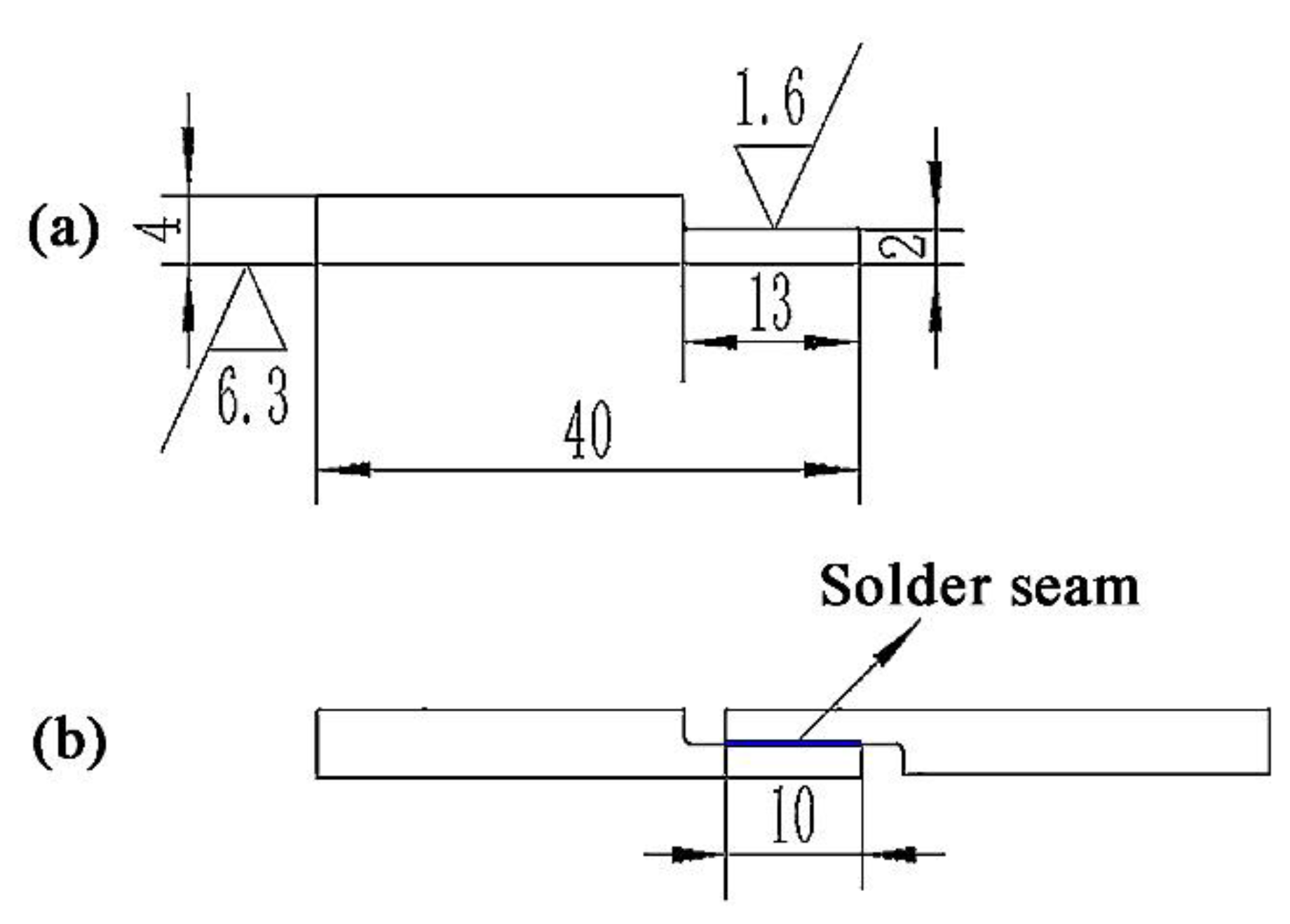
2.1. Materials

To produce the Sn2.5Ag0.7Cu0.1RExNi system solder alloys, the 99.99% pure Sn, Ag, Cu and a mix of Ce to La ratio of 1:1 were used initially to make the alloy. At the beginning, the intermediate alloy of RE and Cu was prepared in non-consumable melting furnace ZHW-600 (Luoyang, China) at a pressure of 5 × 10⁻³ Pa. The Sn2.5Ag0.7Cu0.1RExNi system solder alloy was manufactured at the same condition, while the Ni content was set as 0wt.%, 0.05wt.%, 0.1wt.%, 0.3wt.% and 0.5wt.% separately for each specimen. The parent metal was 99.9% pure copper plate. The soldering flux used was the commercial CX600 water flux.

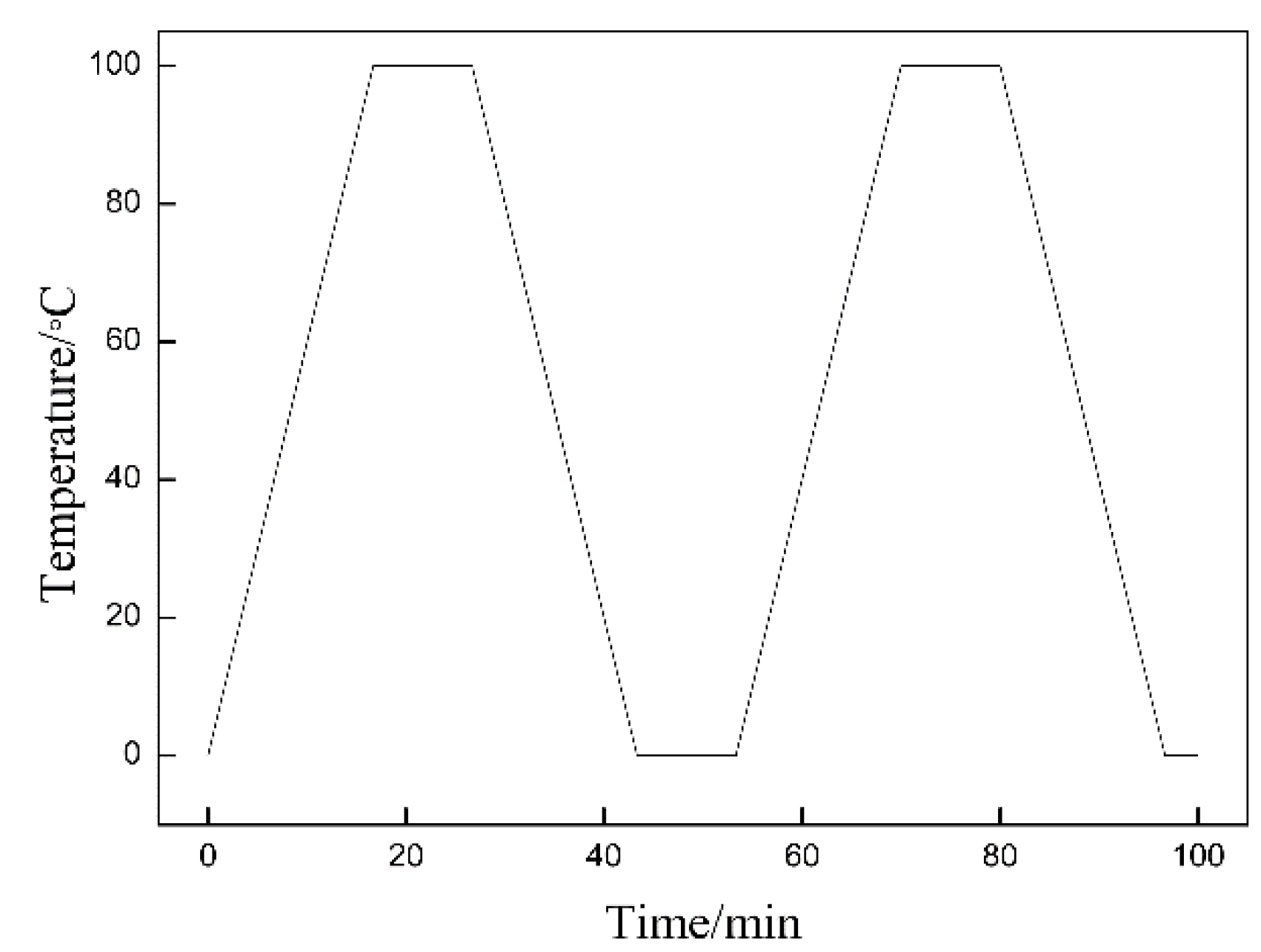
2.2. Methods and Conditions

In methods, in order to keep the solder seam parallel to the Cu substrates surfaces after soldering, special design and measurement for substrates and solder seam were as follows: firstly, the thickness of the Cu substrate is 4 mm, and the thickness of soldering area is 2 mm, as shown in Figure 1a. The substrate surface for soldering was sanded with abrasive paper (#800, #1200, and #1500) and cleaned with acetone. Secondly, the final solder produced was rolled into 10 mm × 20 mm × 0.12 mm strips, then they were sanded with abrasive paper (1500 mesh), the final thick of the solder strips is 0.1 mm, it should be noted that the solder strip was always flat without fold during the process. Thirdly, the 0.1 mm thick solder strip was fixed between two Cu substrates, the solder strip was pressed by upper Cu substrate during soldering. The solder joint is flat as shown in Figure 1b, and the solder seam surfaces were parallel to the substrate surfaces after soldering, eliminating the adverse effect on the shear force values of the solder joints. The soldering experiment was performed in the self-developed soldering furnace. The soldering temperature and time were set at 270 °C, for 240 s.
Thermal-cycle experiments of the solder joints were performed with the SM-KS-50-CC micro-joining joint electrical property tester designed by ourselves, which can change temperatures quickly in a controlled manner. The IPC-9701-a surface mount soldering performance test methods and evaluation standards were followed [25], the experiment is called thermal cycle with the ramping rate below 10 °C/min, and the experiment is called thermal shock with the ramping rate over 10 °C/min. The experiment temperature range for the thermal cycles was set between 0~100 °C, with a ramping rate of 6 °C/min. The dwell time at the high and low temperatures was 10 min. The number of cycles for each experiment was 100, 200, 300, 400, 500 cycles respectively, as is shown in Figure 2. The solder joints following the end of the thermal-cycle experiment were ground, polished, and etched with 4 vol.% nitric acid alcohol solution. The microstructure, composition and morphology of the solder joints were studied by a JMS-5610LV SEM equipped with energy dispersive spectroscopy (EDS) (Japan Electron Optics Laboratory, Tokyo, Japan). The shear tests were carried out in an AG-1250kN tensile testing machine at room temperature. The size of the shear samples was 8 mm × 65 mm ×4 mm and the deformation speed was set at 1 mm/min. The fracture morphology of the solder joints was studied with SEM. Fracture phase analysis was performed with a D8ADVANCE type XRD. To ensure the accuracy of the shear strength test, three different samples were tested, and the mean shear strength was taken as the shear strength value of the sample.
The micro-joining joints interface thickness and roughness is shown in Figure 3 by applying the principle of equal area [26]. The thickness of interfacial IMC layer (d) was measured by using the following Equation (1) the average thickness is used as the roughness measurement datum identified as a dotted line in Figure 3. The interface roughness of the IMC layer with a micro interface contour is characterized by its roughness (R), which can be estimated from Equation (2). Zi in Equation (2) presents the deviation of the peaks or troughs of the interface from the average thickness d of the IMC as shown in Figure 3. To reduce measurement error, five random measurement places were selected and the finally result was expressed as the average of these measurements.
d = A/L
where d is the IMC layer thickness, A is the total area of the IMC layer and L is the length of the coverage.
R = i = 1 N Z i 2 N
where N is the total number of deviations Zi (N=1, 2, 3, i, ……N)

3. Results and Discussion

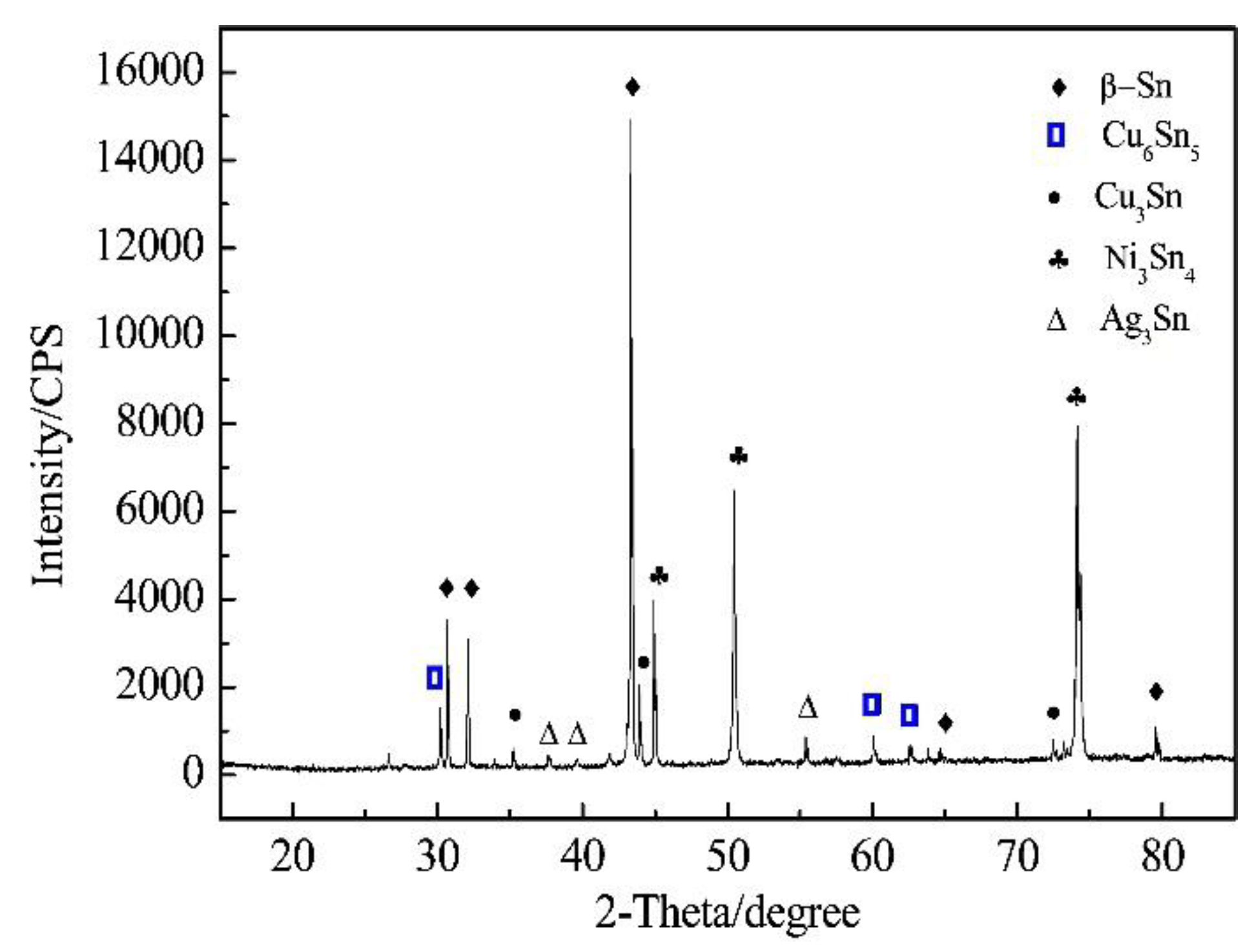
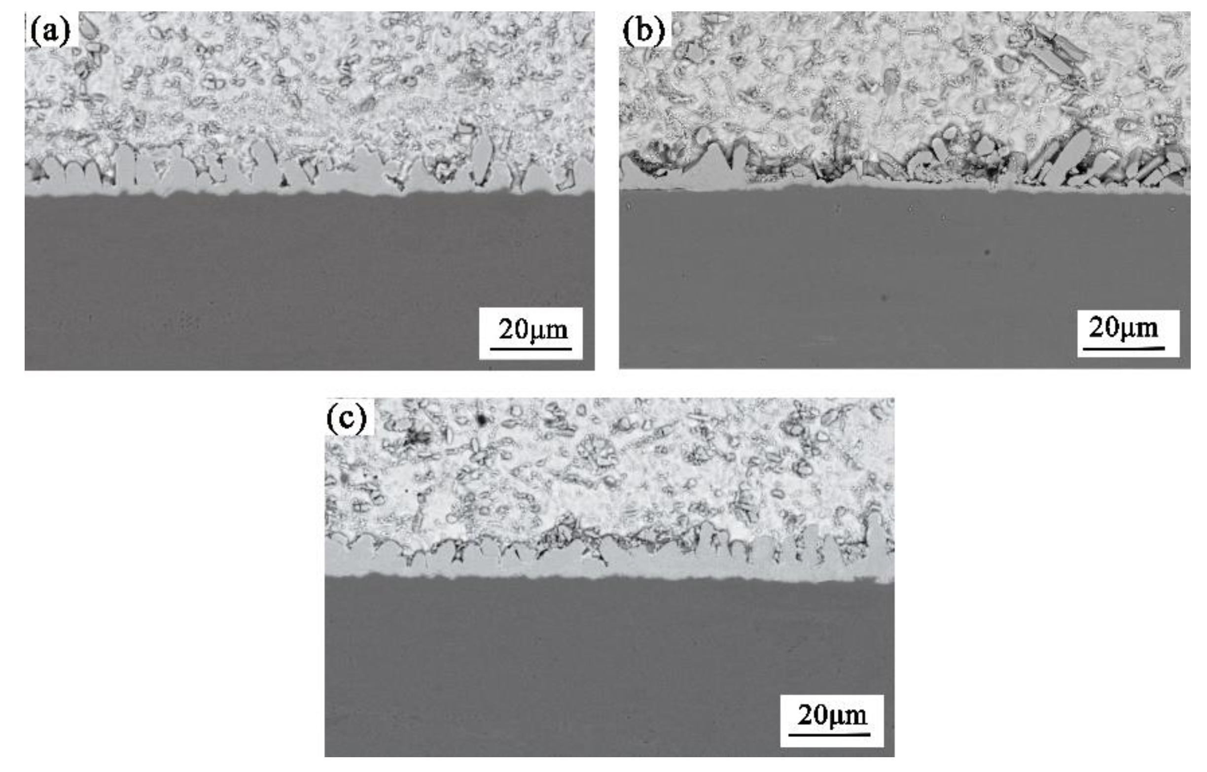
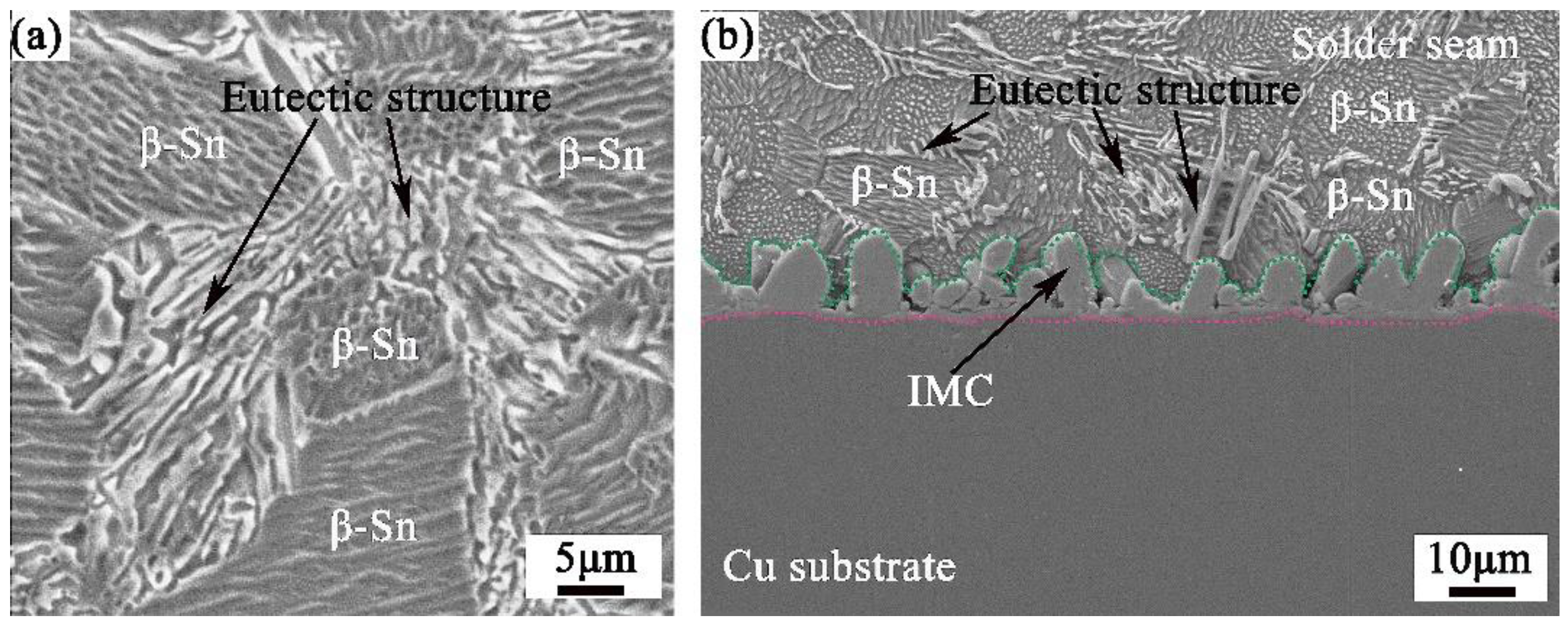
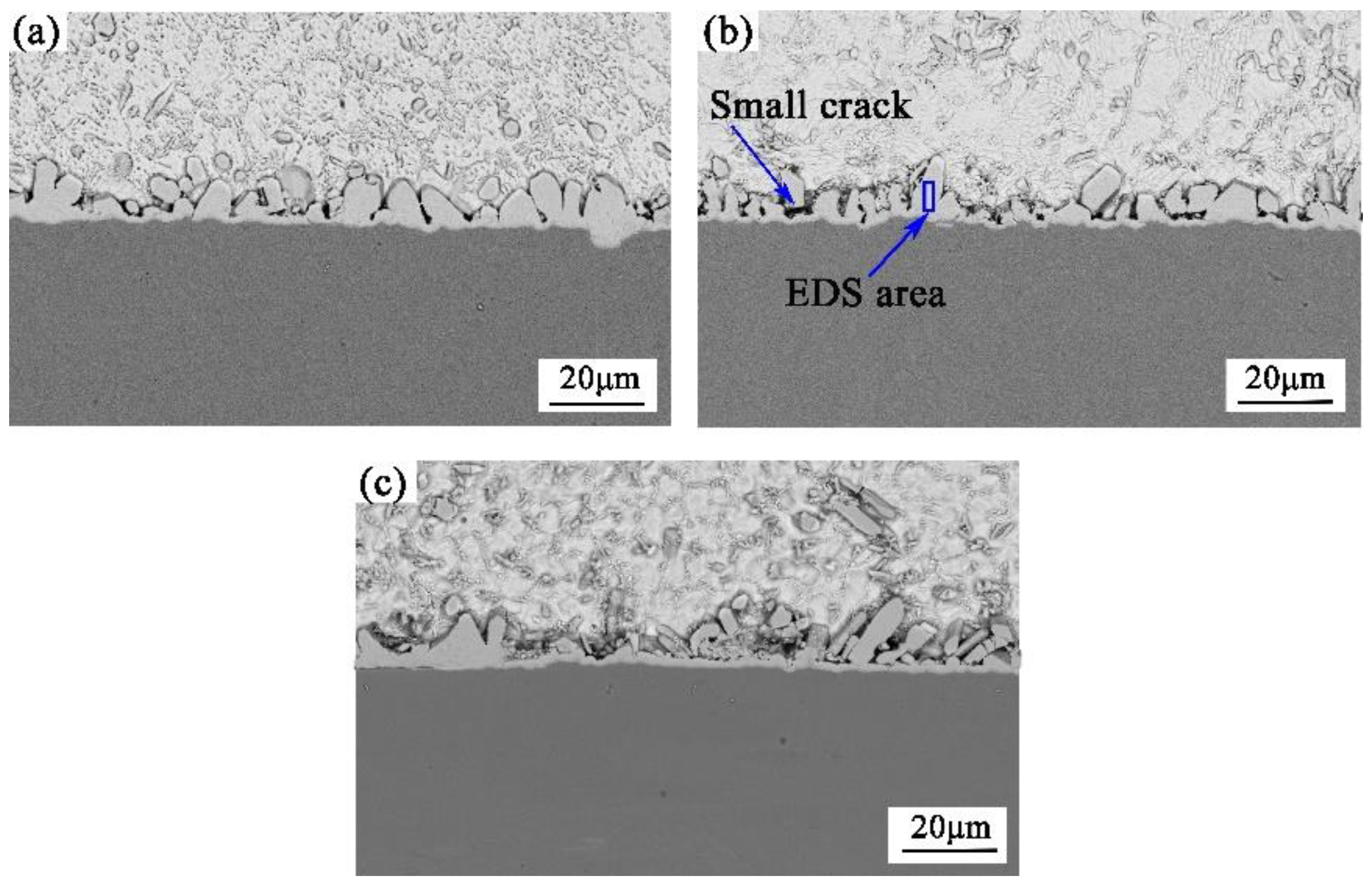
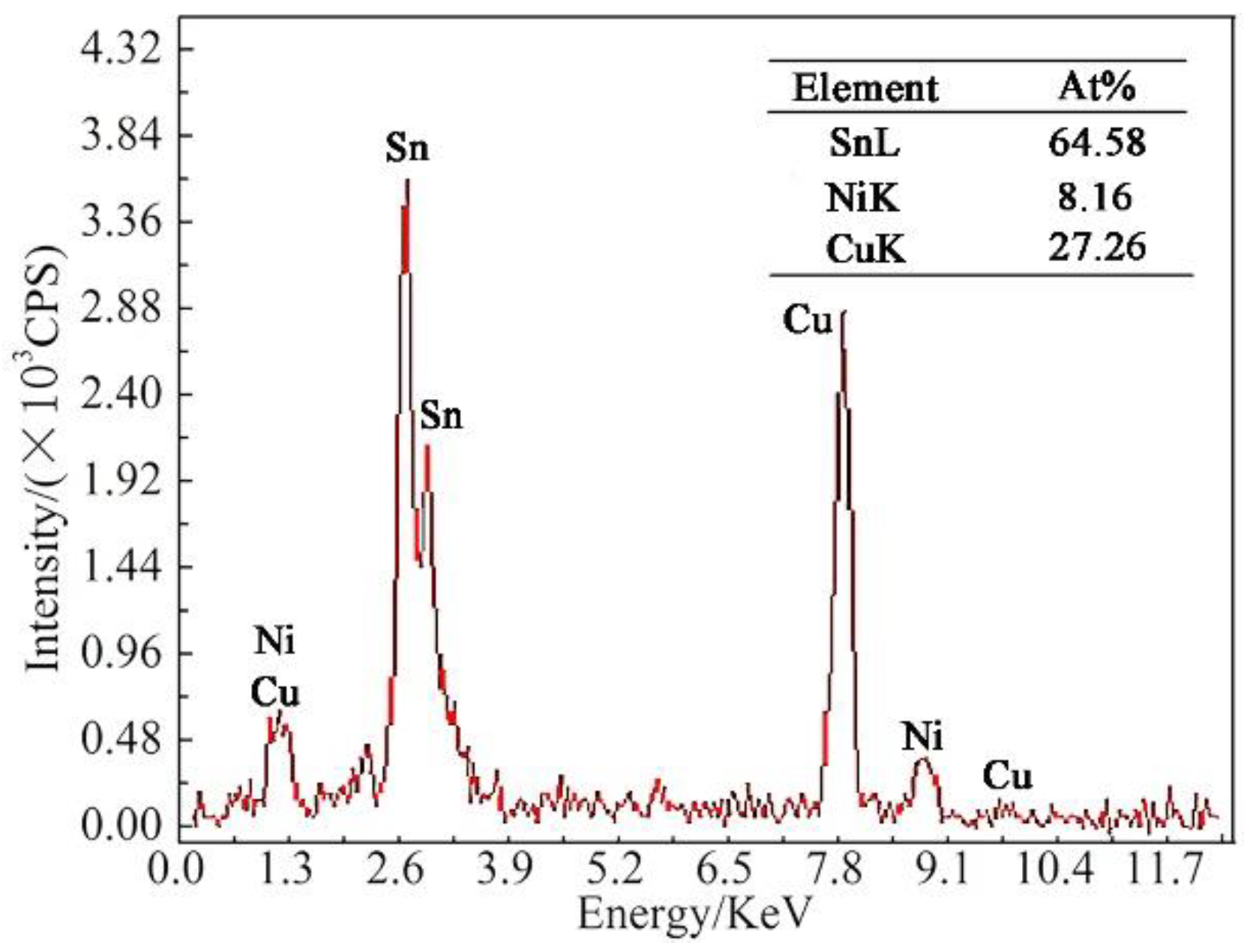
3.1. Microstructure of Sn2.5Ag0.7Cu0.1RExNi/Cu Solder Joints after Thermal-Cycle Loading

The solder seam and interface microstructures of Sn2.5Ag0.7Cu0.1RE0.05Ni/Cu solder joint before thermal cycles are shown in Figure 4. The solder joints were composed of the solder seam, the interface (IMC) and Cu substrate. From the SnAgCu ternary alloy phase diagram, it can be seen that the solder seam area mainly consisted of the spherical or ovoid primary β-Sn and eutectic structure which are distributed around primaryβ-Sn as shown in Figure 4a,b. The IMC locates at the interface of solder seam and Cu substrate, and it grows towards the solder seam as shown in Figure 4b. Previous research has shown that the interface IMC morphology and the dimension of a lead-free solder joint influenced performance and reliability [27]. In this paper, the average thickness (d) and the roughness (R) of the IMC layer are used to characterize the morphology and size of interface IMC, and investigate its effect on the reliability of the solder joints.
The average thickness and the roughness of Sn2.5Ag0.7Cu0.1RE0.05Ni/Cu solder joint are about 3.7 μm and 2.2 μm. Up to now, the Sn2.5Ag0.7Cu0.1RE0.05Ni solder was systematically studied by Zhang Keke's research group. The research includes process optimization [28], the methods (with ultrasound and electric field) improving the strength of the joint [27,29], as well as thermal shock of the Sn2.5Ag0.7Cu0.1RE0.05Ni/Cu joints [30,31], The Sn2.5Ag0.7Cu0.1RE0.05Ni/Cu joints were obtained with the soldering temperature 270 °C and the soldering time 240 s. The IMC thickness of the Sn2.5Ag0.7Cu0.1RE0.05Ni/Cu joints with same soldering technological parameter ranges from 3 and 4.3 μm [27,28,29,30,31], and the roughness of the Sn2.5Ag0.7Cu0.1RE0.05Ni/Cu joints ranges from 1.6 and 2.6 μm [27,29,30,31]. The IMC thickness and the roughness of the Sn2.5Ag0.7Cu0.1RE0.05Ni/Cu joints are little different though with the same soldering parameter. However, the IMC thickness and roughness in this paper are consistent with most results of researchers of our group.
The interface microstructures of Sn2.5Ag0.7Cu0.1RE0.05Ni/Cu solder joints after thermal-cycle loading are shown in Figure 5. The EDS analysis of the interface in Figure 5b is shown in Figure 6, the IMC is composed of Sn, Cu, and Ni. The XRD analysis of the fracture solder joint interface after 300 thermal cycles is shown in Figure 7. With EDS and XRD analysis, the interface is composed of Cu6Sn5, Cu3Sn, and Ni3Sn4, shorting for Cu-Ni-Sn-IMC. The irregular scalloped IMC grew irregularly into solder seam away from the Cu substrate interface.

3.1.1. Effect of Thermal-Cycle Loading

The relationship between the Sn2.5Ag0.7Cu0.1RExNi/Cu soldering joint interface area IMC layer roughness (R), average thickness (d) and thermal-cycle loading is shown in Figure 8. The roughness (R) and average thickness (d) of interface IMC layer in solder joints are proportional to the number of thermal cycles applied to the specimen, up to 300 cycles but the rate of increase decreases sharply from the 300 cycles up to 500 cycles reaching almost a plateau. During thermal-cycle loading, diffusion of Sn, Cu, and Ni atoms contributes to the growth of interface IMC layer. As this interface IMC layer grows into the internal scalloped IMC, the internal scalloped IMC itself grows into the solder seam producing gradually larger, small cracks (Figure 5b), and other defects such as pores. They are created as scalloped IMCs are quickly generated while Cu diffuses into the interface with the IMC at the bottom of these scalloped structures. Dynamic recrystallization in the solder seam under thermal-cycle loading, leads to a reaction of Cu with Sn, Ni atoms while accelerating the growth of interfacial IMC [32].
When the number of thermal cycles increased from 300 to 500, a thick IMC layer which had grown at the beginning of the thermal-cycle loading hindered the diffusion of Cu atoms to the interface area. This increased slowly the roughness and average thickness of the interface IMC layer in soldered joints.

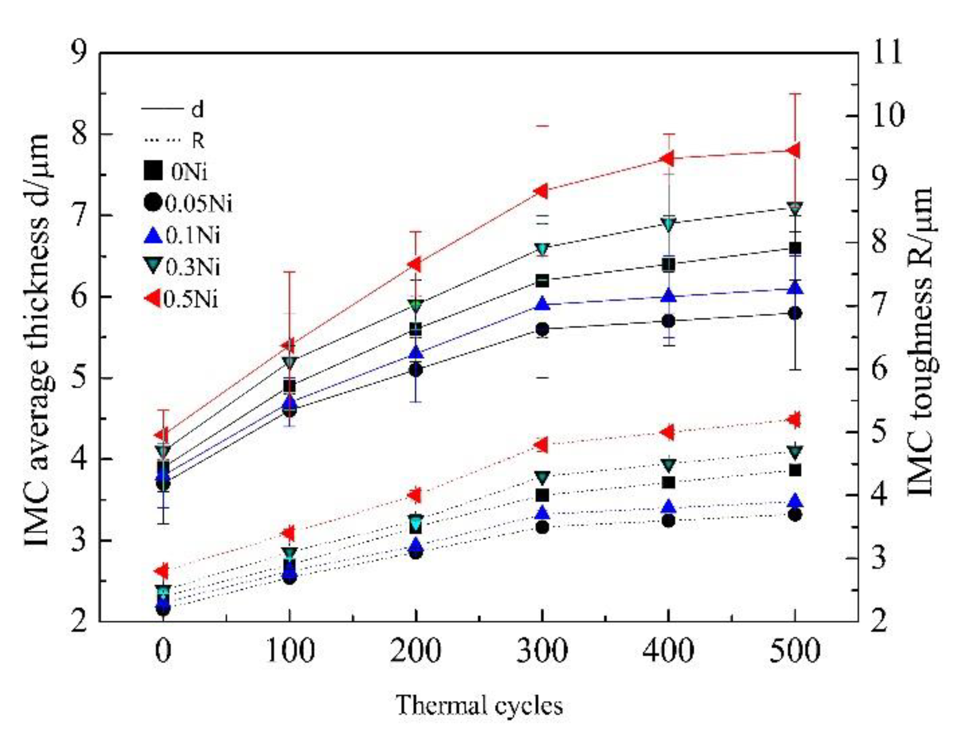
3.1.2. Effect of Ni Content

The interface IMC microstructure of Sn2.5Ag0.7Cu0.1RExNi/Cu solder joints after 500 thermal cycles is shown in Figure 9. The size of interface single scalloped IMC in the solder joint is larger when no Ni is added. The embedded soldering seam with 0.05wt.% Ni added is shorter than that without adding Ni and the interface single scalloped IMC size in that case is the smallest, of the three Ni cases (0 Ni, 0.05 Ni and 0.5 Ni), while the average thickness of which is smallest. This is consistent with the results that the interface roughness and average thickness of Sn2.5Ag0.7Cu0.1RE0.05Ni/Cu solder joints is lowest under thermal-cycle loading as shown in Figure 8. At the same time, it can be seen from Figure 8 that the interface IMC layer roughness and average thickness of Sn2.5Ag0.7Cu0.1RE0.05Ni/Cu solder joins and Sn2.5Ag0.7Cu0.1RE0.1Ni/Cu solder joins are both smaller than those of not adding Ni in solder joints under thermal cycles. It appears that the addition of a suitable amount of Ni into the Sn2.5Ag0.7Cu0.1RE/Cu solder joints can restrain growth of interfacial IMC under thermal-cycle loading. This must be associated with the small solubility of Ni in the Sn-based lead-free solder and the small reaction rate of Ni-Sn IMC. Adding a suitable amount of Ni increases the resistance of interface element diffusion, reducing generation rate of interface IMC and inhibiting the growth of IMC.

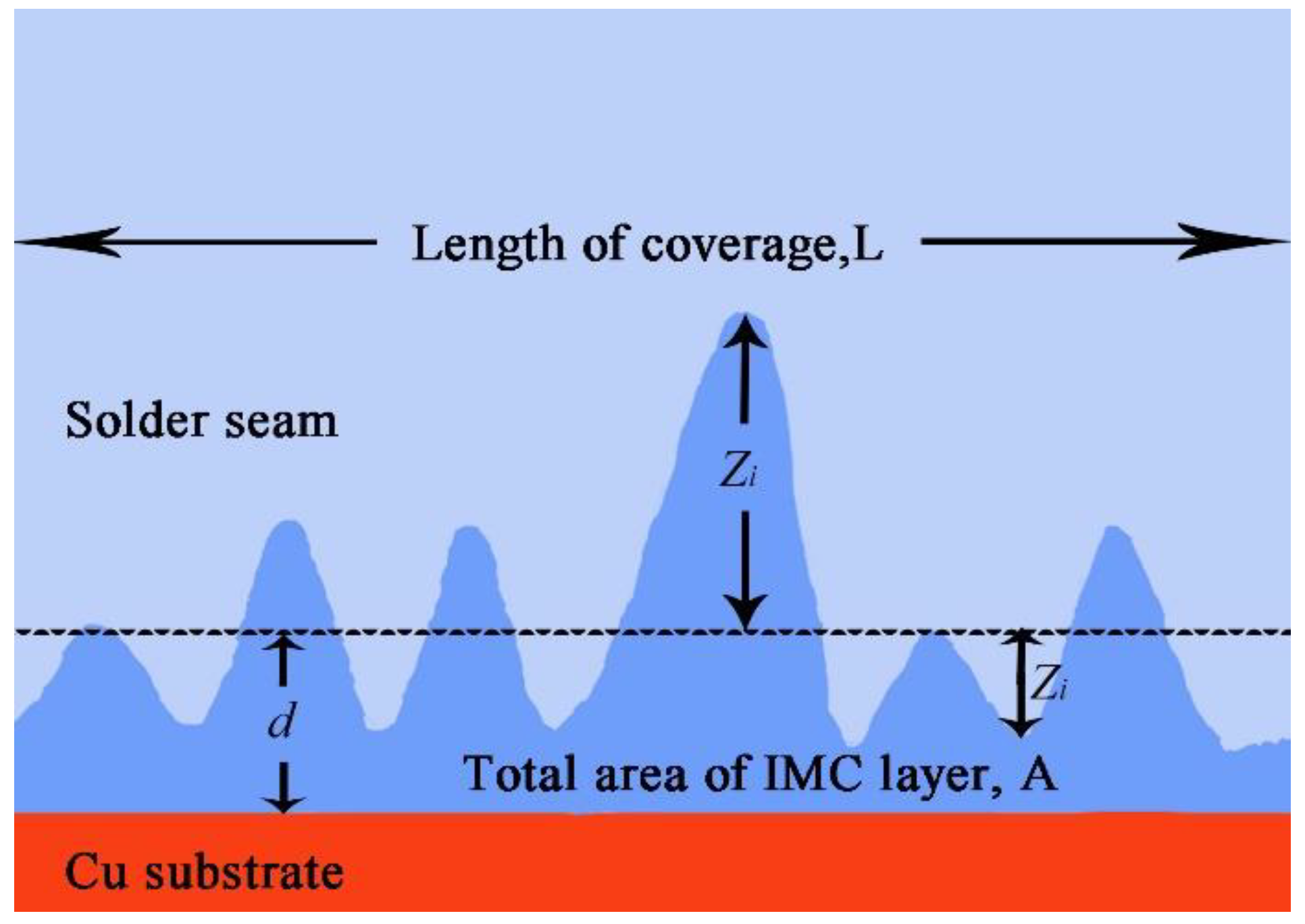
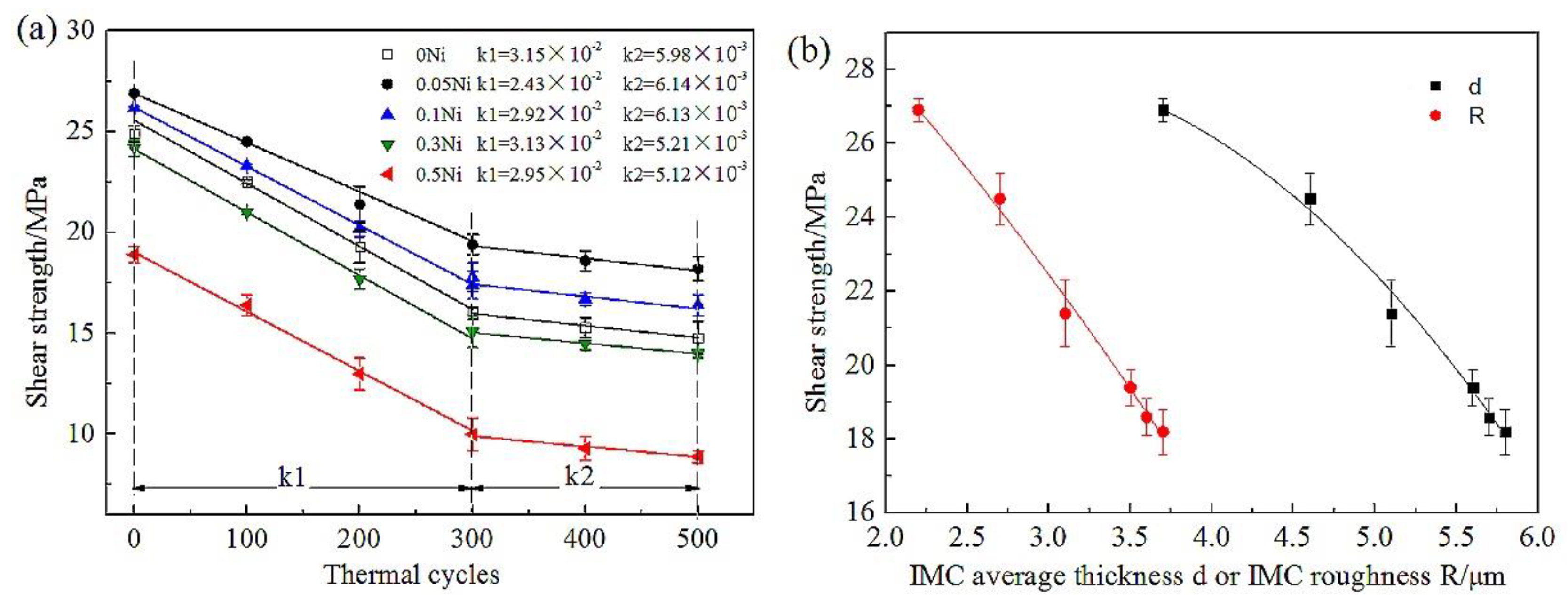
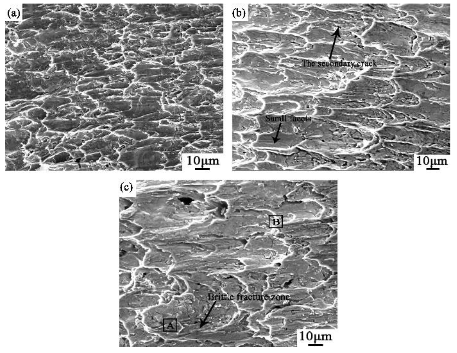
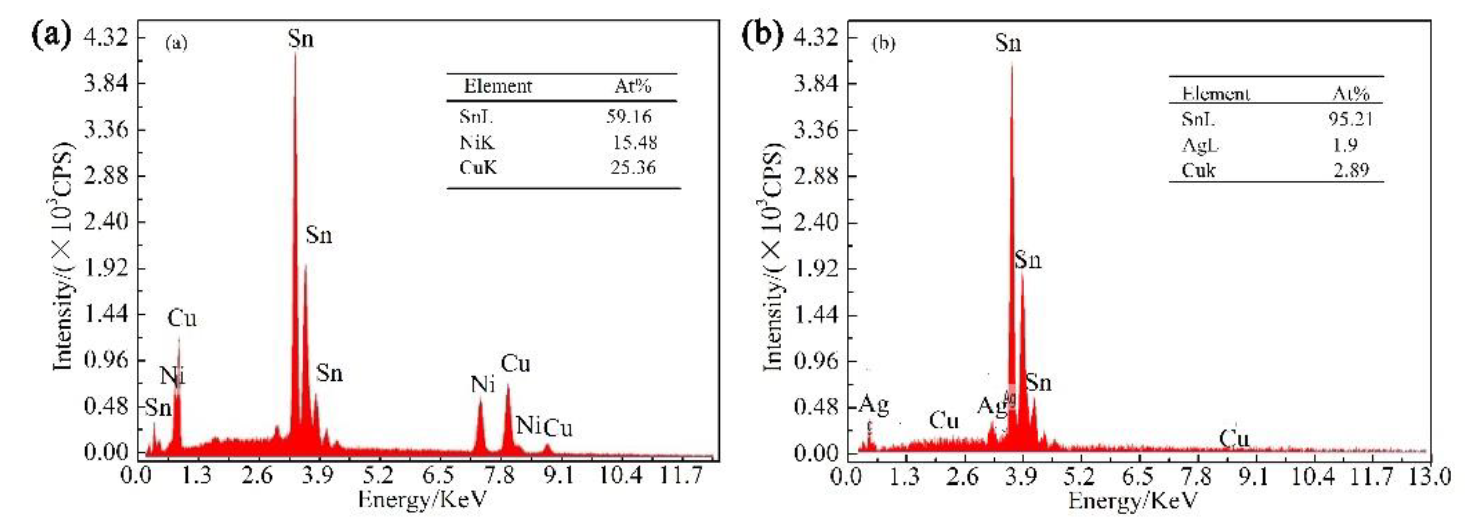
3.2. Shear Strength of Sn2.5Ag0.7Cu0.1RExNi/Cu Solder Joints under Thermal-Cycle Loading

The shear strength of the Sn2.5Ag0.7Cu0.1RExNi/Cu solder joints under different number of thermal cycles, and their average thickness (IMC d) and roughness (IMC R) is shown in Figure 10. It can be seen from Figure 10a that shear strength decreases with the number of thermal cycles applied up to 300 thermal cycles, and this rate of decrease changes following the 300 thermal-cycle limit (the slope k2 of the fitted line from 300 to 500 thermal cycles is about 1/4 to 1/6 of the slope k1 of the first part of the line up to 300 cycles). In the end, the shear strength of the solder joint has decreased about 40% after 500 thermal cycles. The shear strength of Sn2.5Ag0.7Cu0.1RExNi/Cu solder joints under thermal-cycle loading is closely related to the Ni content. The shear strength of the soldered joint with less than 0.1 wt.% Ni is higher than that of the soldered joint without any Ni. The shear strength of Sn2.5Ag0.7Cu0.1RE0.05Ni/Cu solder joint under 500 thermal-cycle loading was reduced to 36.4% of that with no thermal loading, which equals 18.2MPa. Out of the five cases of Ni content, i.e., from 0 up to 0.5% Ni, the highest shear strength achieved at the end of the 500 thermal-cycle loading was for the 0.05% Ni case. From Figure 10b, the relationship between the shear strength of soldered joints and average thickness of the interfacial IMC layer follows a quadratic power function, while the relationship between shear strength of soldering joints and roughness of the interfacial IMC layer follows a linear function. As less interface IMC is formed, the lower of the average thickness and roughness produced, and lower the toughness of solder joints obtained. When comparing Figure 8 and Figure 9, the roughness and average thickness of the interface IMC layer in Sn2.5Ag0.7Cu0.1RE0.05Ni/Cu solder joints is lowest under all thermal-cycle loads, which is consistent with the fact observed in Figure 10b that the shear strength of the joint is inversely proportional to average thickness and roughness of the IMC layer. Hence, the addition of a moderate amount of Ni suppresses the decline of shear strength of soldered joints under thermal-cycle loading.
The shear fracture morphology of Sn2.5Ag0.7Cu0.1RE0.05Ni/Cu soldered joints during thermal-cycle loading process is shown in Figure 11. The nest “parabola” dimples of various sizes were observed on the shear fracture surface after 100 thermal cycles, which illustrates a ductile mode of fracture occurring in the solder seam. As the number of thermal cycles increases, the nest dimples of shear fracture elongate and reduce in numbers gradually, which induce secondary cracks and short flat small face fracture appears on part of the fracture surface after 300 thermal cycles. As more thermal cycles continue to be applied, a small number of “mountain” dimples with larger size but shallow appear, together with a small brittle fracture zone after 500 thermal cycles. This means that the fracture mechanism of Sn2.5Ag0.7Cu0.1RExNi/Cu soldered joints changes gradually from a ductile to a mixed ductile-brittle fracture pattern as the number of thermal cycles increase. EDS analysis of areas A and B in Figure 11c is shown in Figure 12. Based on the SEM observation and EDS analysis result, ductile fracture with parabolic dimples was observed in region B, where the composition on the surface was mainly composed of Sn element, while brittle fracture appeared in region A which is mainly composed of Cu6Sn5 and Ni3Sn4 IMC.
The fracture mechanism and crack initiation site changed with the number of thermal cycles applied up to 500 thermal cycles. The schematic drawing illustrates of fracture model are shown in Figure 13. As the thermal cycle increased, the fracture pathway evolved from the ductile fracture of the solder seam (P1) to the ductile-brittle mixed-type fracture of solder seam/IMC layer (P2).
The shear fracture microstructure of Sn2.5Ag0.7Cu0.1RExNi/Cu solder joints for different Ni content after 300 thermal cycles is shown in Figure 14. The shear fracture morphology of the solder joints has “deformed dimples”, “parabola” fracture nest dimples, together with partial cleavage. From the shear fracture morphology of the solder joints adding Ni up to 0.05% has the effect of increasing the number and elongating the dimples (Figure 14a,b), while further increases in Ni content reduce their number while increasing their size (Figure 14b,c). The fracture morphology changed to a cleavage pattern. Therefore, adding Ni in the solder up to 0.05% transformed the way of shear fracture in soldering joints under the thermal-cycle loading, and improved the reliability of solder joints in the end.

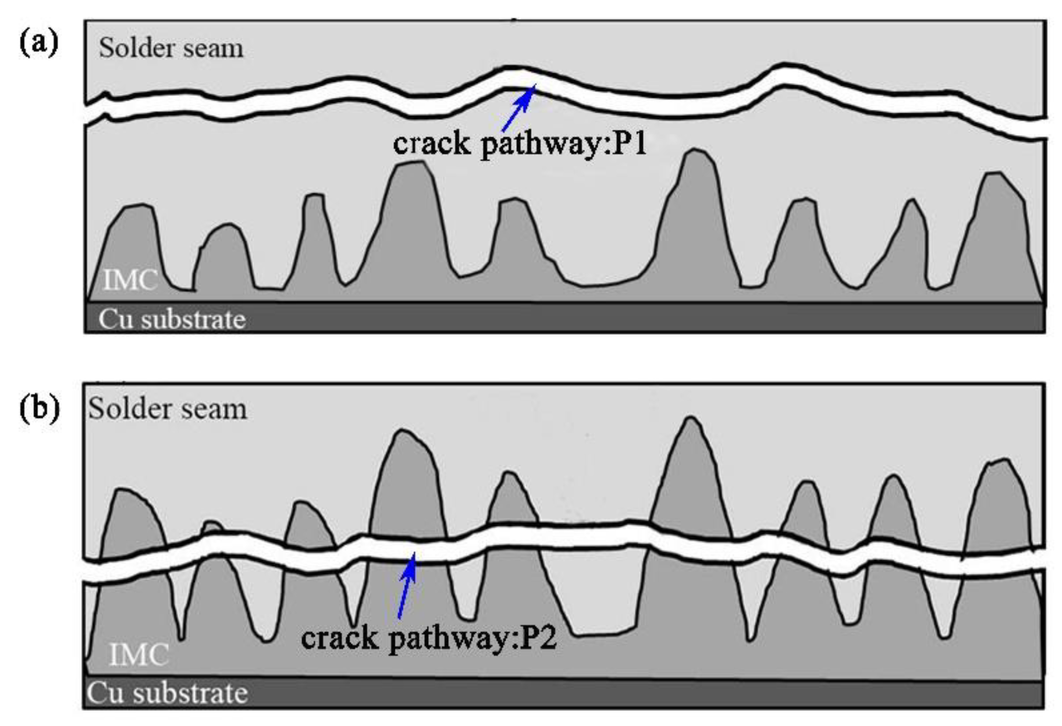
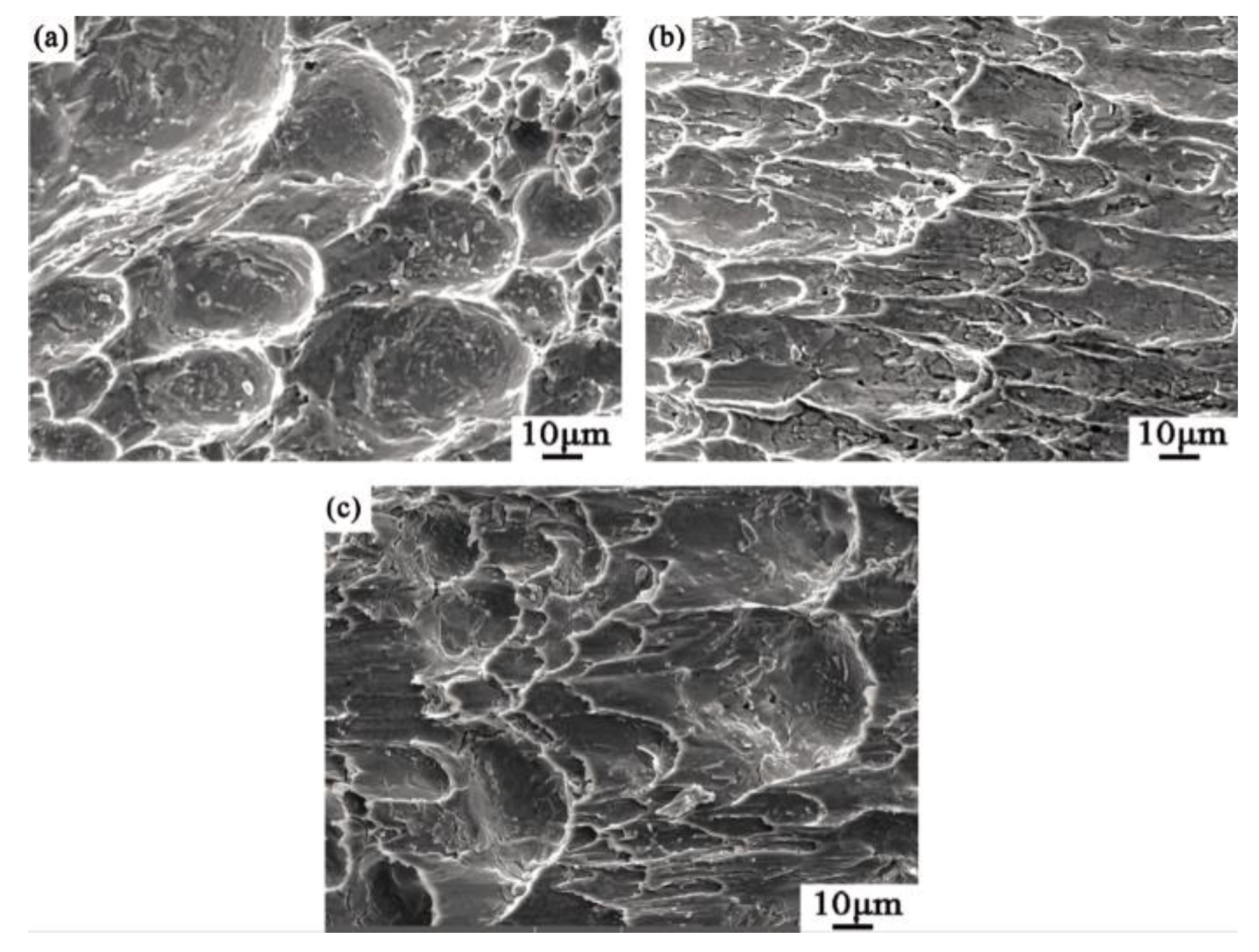
3.3. Analysis and Discussion

In the process of thermal-cycle loading, Sn2.5Ag0.7Cu0.1RExNi/Cu solder joints were under continuous non-uniform thermal loadings (ranging from 0 to 100 °C). The low melting point of Sn2.5Ag0.7Cu0.1RExNi system lead-free solder obviously affects the microstructure and mechanical properties of such solder joints. Microstructure and performance of these joints at the interface area are closely related to the morphology and size of interfacial IMCs and atomic diffusion during those thermal cycles [33,34]. Interface Cu atoms react with interface Sn and Ni atoms to generate Cu3Sn, Cu6Sn5 and Ni3Sn4. The IMC layer evolves into scalloped IMC in a gradual manner while introducing crystalline defects such as grain boundaries and dislocations, followed by growth into the solder seam. A new IMC is generated between the scalloped grooves where it is easier for Cu atoms to diffuse. This is followed by the IMC growing large. The roughness and average thickness of the interface IMC increases with the number of thermal cycles. As the thermal expansion coefficient is different in the various areas of the solder joint micro-cracks form and extent into the interface area. As the joint is under accumulated thermal stress during the thermal-cycle loading, its shear strength is reduced. At the same time, fracture characteristics of the solder joints gradually changes from ductile fracture in the solder seam to a mixed mode fracture where there is brittle fracture at the interface IMC layer and ductile fracture in the solder seam, with the increase of thermal cycles. This affects joint reliability accordingly.
The atomic number and crystal lattice structure of Ni are closer to that of Cu; however, the rate of dissolution and diffusion of Ni in the Sn-based lead-free solder is slower than that of Cu. The reaction activation energy of Ni and Sn is lower than that of Cu and Sn, so the Ni-Sn IMC reaction rate is lower than that of Cu-Sn [35]. By adding suitable amounts of Ni will increase the interface element diffusion resistance, while reduce the generation rate of the interface IMC in solder joints, which will inhibit IMC quick growth. An appropriate amount of Ni, added to Sn2.5Ag0.7Cu0.1RE solder alloy, can significantly refine the primary β-Sn phase and eutectic structure in the solder seam, while inhibit the growth of Cu6Sn5 IMC in solder joints at the interface area. In the end, the microstructure of the interface zone IMC and the shear fracture morphology of solder joints were improved, where high shear strength and remarkable reliability solder joints were obtained.

4. Conclusions

The following conclusions were made from the study of IMC of Sn2.5Ag0.7Cu0.1RExNi/Cu solder joins under thermal cycles:
(1) With thermal-cycle loading increasing from 0 to 500 cycles, the shape of interfacial IMC layer of Sn2.5Ag0.7Cu0.1RExNi/Cu solder joints gradually evolves from scalloped to large wavy form, and the interface roughness and average thickness of the IMC layer increases. The corresponding shear strength of the solder joints is reduced by 40%. The fracture pathway evolved from the ductile fracture of the solder seam to the ductile-brittle mixed-type fracture of solder seam/IMC layer, when the number of thermal cycles increased from 100 cycle to 500 cycle.
(2) Adding 0.05 wt.% Ni can inhibit the growth of the interface IMC of Sn2.5Ag0.7Cu0.1RE/Cu solder joints under thermal-cycle loading, and decrease the average thickness and roughness of the interface IMC layer; the shear strength of solder joints is higher than that without Ni. The roughness and average thickness of the interface IMC layer in Sn2.5Ag0.7Cu0.1RE0.05Ni/Cu solder joints is lowest under thermal-cycle loading, the shear strength of such solder joints under 500 thermal cycles is reduced to a minimum of 36.4% of the initial value of the unloaded case, reaching a shear strength value of 18.2 MPa.

Author Contributions

C.C. and K.Z. conceived and designed the experiments; D.Z. and M.S. contributed to the process of the preparation of samples; C.Z. analyzed the date; C.C. wrote the paper; B.S. and H.W. revised the paper; Funding Acquisition, K.Z.

Funding

This research was funded by the National Natural Science Foundation of China (U1604132), the Plan for Scientific Innovation Talent of Henan Province, China (154200510022) and Collaborative Innovation Center of Nonferrous Metals, Henan Province, China.

Conflicts of Interest

The authors declare no conflict of interest.

References

  1. Gain, A.K.; Zhang, L.; Chan, Y.C. Microstructure, elastic modulus and shear strength of alumina (Al2O3) nanoparticles-doped tin-silver-copper (Sn-Ag-Cu) solders on copper (Cu) and gold/nickel (Au/Ni)-plated Cu substrates. J. Mater. Sci.-Mater. Electron. 2015, 26, 7039–7048. [Google Scholar] [CrossRef]
  2. Gain, A.K.; Zhang, L. Interfacial microstructure, wettability and material properties of nickel (Ni) nanoparticle doped tin-bismuth-silver (Sn-Bi-Ag) solder on copper (Cu) substrate. J. Mater. Sci.-Mater. Electron. 2016, 27, 3982–3994. [Google Scholar] [CrossRef]
  3. Gnecco, F.; Ricci, E.; Amore, S.; Borzone, G.; Novakovic, R. Wetting behaviour and reactivity of lead free Au–In–Sn and Bi–In–Sn alloys on copper substrates. Int. J. Adhes. Adhes. 2007, 27, 409–416. [Google Scholar] [CrossRef]
  4. Gain, A.K.; Zhang, L.; Quadir, M.Z. Thermal aging effects on microstructures and mechanical properties of an environmentally friendly eutectic tin-copper solder alloy. Mater. Des. 2016, 110, 275–283. [Google Scholar] [CrossRef]
  5. Kotadia, H.R.; Howes, P.D.; Mannan, S.H. A review: On the development of low melting temperature Pb-free solders. Microelectron. Reliab. 2014, 54, 1253–1273. [Google Scholar] [CrossRef]
  6. Gain, A.K.; Zhang, L. Microstructure, thermal analysis and damping properties of Ag and Ni nano-particles doped Sn-8Zn-3Bi solder on OSP-Cu substrate. J. Alloys Compd. 2014, 617, 779–786. [Google Scholar] [CrossRef]
  7. Gain, A.K.; Zhang, L. Growth mechanism of intermetallic compound and mechanical properties of nickel (Ni) nanoparticle doped low melting temperature tin–bismuth (Sn–Bi) solder. J. Mater. Sci.-Mater. Electron. 2016, 27, 781–794. [Google Scholar] [CrossRef]
  8. Chan, Y.C.; Yang, D. Failure mechanisms of solder interconnects under current stressing in advanced electronic packages. Prog. Mater. Sci. 2010, 55, 428–475. [Google Scholar] [CrossRef]
  9. Gain, A.K.; Zhang, L. Microstructure, mechanical and electrical performances of zirconia nanoparticles-doped tin-silver-copper solder alloys. J. Mater. Sci.-Mater. Electron. 2017, 27, 7524–7533. [Google Scholar] [CrossRef]
  10. Zhang, L.; Tu, K.N. Structure and properties of lead-free solders bearing micro and nano particles. Mater. Sci. Eng. R. 2014, 82, 1–32. [Google Scholar] [CrossRef]
  11. Gain, A.K.; Zhang, L. Harsh service environment effects on the microstructure and mechanical properties of Sn-Ag-Cu-1 wt% nano-Al solder alloy. J. Mater. Sci.-Mater. Electron. 2016, 27, 11273–11283. [Google Scholar] [CrossRef]
  12. Zhang, L.; Xue, S.B.; Zeng, G.; Gao, L.L.; Ye, H. Interface reaction between SnAgCu/SnAgCuCe solders and Cu substrate subjected to thermal cycling and isothermal aging. J. Alloys Compd. 2012, 510, 38–45. [Google Scholar] [CrossRef]
  13. Zhang, L.; Fan, X.Y.; Guo, Y.H.; He, C.W. Properties enhancement of SnAgCu solders containing rare earth Yb. Mater. Des. 2014, 57, 646–651. [Google Scholar] [CrossRef]
  14. Li, G.; Shi, Y.; Hao, H.; Xia, Z.; Lei, Y. Effect of rare earth addition on shear strength of SnAgCu lead-free solder joints. J. Mater. Sci.-Mater. Electron. 2009, 20, 186–192. [Google Scholar] [CrossRef]
  15. Zhang, K.K.; Zhang, X.J.; Qiu, R.F.; Shi, H.X.; Liu, Y.J. The combined effects of ultrasonic wave and electric field on the microstructure and properties of Sn2.5Ag0.7Cu0.1RE/Cu soldered joints. J. Mater. Sci.-Mater. Electron. 2014, 25, 1681–1686. [Google Scholar] [CrossRef]
  16. El-Daly, A.A.; El-Taher, A.M. Evolution of thermal property and creep resistance of Ni and Zn-doped Sn-2.0Ag-0.5Cu lead-free solders. Mater. Des. 2013, 51, 789–796. [Google Scholar] [CrossRef]
  17. Tao, Q.B.; Benabou, L.; Le, V.N.; Wang, H.; Lu, D.B. Viscoplastic characterization and post-rupture microanalysis of a novel lead-free solder with small additions of Bi, Sb and Ni. J. Alloys Compd. 2016, 694, 892–904. [Google Scholar] [CrossRef]
  18. Park, Y.; Bang, J.H.; Oh, C.M.; Hong, W.S.; Kang, N. Effect of eutectic structure on creep properties of Sn-3.0Ag-0.5Cu and Sn-8.0Sb-3.0Ag solders. Metals 2017, 7, 540. [Google Scholar] [CrossRef]
  19. Li, S.; Yan, Y.F. Intermetallic growth study at Sn-3.0Ag-0.5Cu/Cu solder joint interface during different thermal conditions. J. Mater. Sci.-Mater. Electron 2015, 26, 9470–9477. [Google Scholar] [CrossRef]
  20. Zhang, K.K.; Li, C.Y.; Qiu, R.F.; Shi, H.X.; Wang, Y.L. Effect of Ni on growing of intermetallic compound in interface of Sn2.5Ag0.7Cu0.1RE/Cu solder joint during aging. Mater. Sci. Technol. 2012, 28, 760–765. [Google Scholar] [CrossRef]
  21. Xiao, H.; Li, X.Y.; Hu, Y.; Guo, F.; Shi, Y.W. Damage behavior of SnAgCu/Cu solder joints subjected to thermomechanical cycling. J. Alloys Compd. 2013, 578, 110–117. [Google Scholar] [CrossRef]
  22. Han, Y.D.; Jing, H.Y.; Nai, S.M.L.; Xu, L.Y.; Tan, C.M. Interfacial reaction and shear strength of Ni-coated carbon nanotubes reinforced Sn-Ag-Cu solder joints during thermal cycling. Intermetallics 2012, 3, 72–78. [Google Scholar] [CrossRef]
  23. Zhou, Q.; Zhou, B.; Lee, T.K.; Bieler, T. Microstructural evolution of SAC305 solder joints in wafer level chip-scale packaging (WLCSP) with continuous and interrupted accelerated thermal cycling. J. Electron. Mater. 2016, 45, 3013–3024. [Google Scholar] [CrossRef]
  24. Bang, J.; Yu, D.Y.; Yang, M.; Ko, Y.H.; Yoon, J.W.; Nishikawa, H.; Lee, C.W. Improvement in thermomechanical reliability of low cost Sn-Based BGA interconnects by Cr Addition. Metals 2018, 8, 586. [Google Scholar] [CrossRef]
  25. IPC-9701. Performance Test Methods and Qualification Requirements for Surface Mount Solder Attachments; IPC: Northbrook, IL, USA, 2002. [Google Scholar]
  26. Yu, D.Q.; Wang, L. The growth and roughness evolution of intermetallic compounds of Sn-Ag-Cu/Cu interface during soldering reaction. J. Alloys Compd. 2008, 458, 542–547. [Google Scholar] [CrossRef]
  27. Zhao, D.; Zhang, K.; Cui, J.; Ma, N.; Pan, Y.; Yin, C. Effect of ultrasonic vibration on the interfacial IMC three-dimensional morphology and mechanical properties of Sn2.5Ag0.7Cu0.1RE0.05Ni/Cu halogen free solder joints. J. Mater. Sci.-Mater. Electron. 2018, 29, 18828–18839. [Google Scholar] [CrossRef]
  28. Li, C.Y.; Zhang, K.K.; Wang, Y.L.; Zhao, K.; Du, Y.L. Effect of Ni on interfacial IMC and mechanical properties of Sn2.5Ag0.7Cu0.1RE/Cu solder joints. Trans. China Weld. Inst. 2012, 33, 39–42. (In Chinese) [Google Scholar]
  29. Cui, J.G.; Zhang, K.K.; Zhao, D.; Ma, N.; Cao, C.C.; Pan, Y.B. Microstructure and properties of Sn2.5Ag0.7Cu0.1RE0.05Ni/Cu solder joints obtained by external energy assisted soldering. Rare Metal. Mat. Eng. 2018, 47, 2800–2806. (In Chinese) [Google Scholar]
  30. Guo, X.D.; Zhang, K.K.; Qiu, R.F.; Shi, H.X.; Wang, Y.L.; Ma, N. Effect on interface and property of Sn2.5Ag0.7Cu0.1RExNi/Cu solder joints in severe thermal cycling. Chin. J. Nonferrous. Met. 2016, 26, 2573–2579. (In Chinese) [Google Scholar]
  31. Zhang, K.K.; Guo, X.D.; Wang, H.G. Interfacial microstructure and mechanical properties of Sn2.5Ag0.7Cu0.1RE0.05Ni/Cu solder joint under thermal shock. Rare Metal. Mat. Eng. 2017, 46, 1353–1358. (In Chinese) [Google Scholar]
  32. Shen, J.; Zhao, M.; He, P.; Pu, Y. Growth behaviors of intermetallic compounds at Sn-3Ag-0.5Cu/Cu interface during isothermal and non-isothermal aging. J. Alloys Compd. 2013, 574, 451–458. [Google Scholar] [CrossRef]
  33. Yang, D.; Cai, J.; Wang, Q.; Li, J.; Hu, Y. IMC growth and shear strength of Sn-Ag-Cu/Co-P ball grid array solder joints under thermal cycling. J. Mater. Sci.-Mater. Electron. 2015, 26, 962–969. [Google Scholar] [CrossRef]
  34. Zeng, G.; Mcdonald, S.D.; Mu, D.; Terada, Y.; Yasuda, H. The influence of ageing on the stabilisation of interfacial (Cu,Ni)6(Sn,Zn)5,and(Cu,Au,Ni)6Sn5, intermetallics in Pb-free Ball Grid Array (BGA) solder joints. J. Alloys Compd. 2016, 685, 471–482. [Google Scholar] [CrossRef]
  35. Yang, S.T.; Chung, Y.; Kim, Y.H.; Hong, B.H. Intermetallic growth between Sn-Ag-(Cu) solder and Ni. Proceed. Adv. Electron. Mater. Pack. 2001, 19–22, 219–224. [Google Scholar]
Figure 1. Details of Cu substrate sample (a) and solder joint (b). (Unit: mm)
Metals 09 00518 g001
Figure 2. Thermal cycles.
Metals 09 00518 g002
Figure 3. Typical cross section of a solder joints interfacial IMC layer with an average thickness d and roughness R.
Metals 09 00518 g003
Figure 4. Solder seam (a) and interface microstructure (b) of Sn2.5Ag0.7Cu0.1RE0.05Ni/Cu solder joint before thermal cycles.
Metals 09 00518 g004
Figure 5. Interface SEM morphology of Sn2.5Ag0.7Cu0.1RE0.05Ni/Cu solder joint after thermal cycles. (a) 100 cycles; (b) 300 cycles; (c) 500 cycles.
Metals 09 00518 g005
Figure 6. EDS results of the solder joint interface in Figure 5b.
Metals 09 00518 g006
Figure 7. XRD analysis of fracture after 300 cycles.
Metals 09 00518 g007
Figure 8. Relationship between Sn2.5Ag0.7Cu0.1RexNi/Cu solder joint interface area IMC layer roughness R, average thickness d, and thermal-cycle loading.
Metals 09 00518 g008
Figure 9. Interface IMC microstructure of Sn2.5Ag0.7Cu0.1RExNi/Cu solder joints after 500 thermal cycles. (a) 0Ni; (b) 0.05Ni; (c) 0.5Ni.
Metals 09 00518 g009
Figure 10. Relationship between shear strength and number of thermal cycles (a) and the IMC thickness and roughness (b). (a) Thermal-cycle effect; (b) IMC d and IMC R effect.
Metals 09 00518 g010
Figure 11. Fracture microstructure of Sn2.5Ag0.7Cu0.1RE0.05Ni/Cu solder joints under thermal cycles. (a) 100 cycles; (b) 300 cycles; (c) 500 cycles.
Metals 09 00518 g011
Figure 12. EDS analysis of Sn2.5Ag0.7Cu0.1RExNi/Cu soldering joint under thermal-cycle loading. (a) A area in Figure 11c; (b) B area in Figure 11c.
Metals 09 00518 g012
Figure 13. Schematic drawing illustrates of fracture model. (a) Crack propagation after 100cycle; (b) Crack propagation after 500 cycles.
Metals 09 00518 g013
Figure 14. Shear fracture microstructure of Sn2.5Ag0.7Cu0.1RExNi/Cu solder joint under 300 thermal-cycle loading for different Ni content. (a) 0Ni; (b) 0.05Ni; (c) 0.5Ni.
Metals 09 00518 g014

