
Effects of Isothermal Aging on Interfacial Microstructure and Shear Properties of Sn-4.5Sb-3.5Bi-0.1Ag Soldering with ENIG and ENEPIG Substrates

 and
and 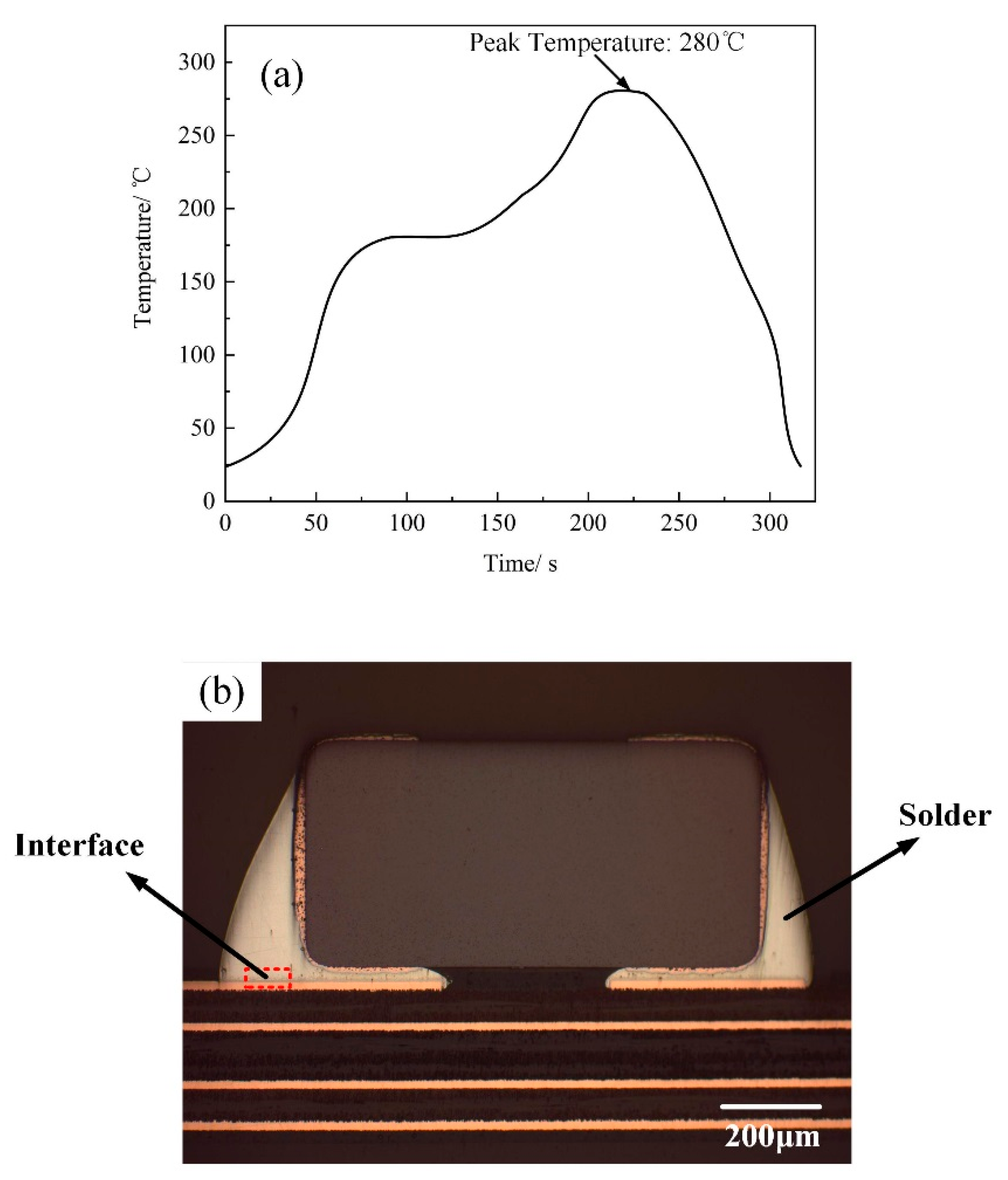
Abstract
:1. Introduction
2. Materials and Methods
3. Results and Discussion
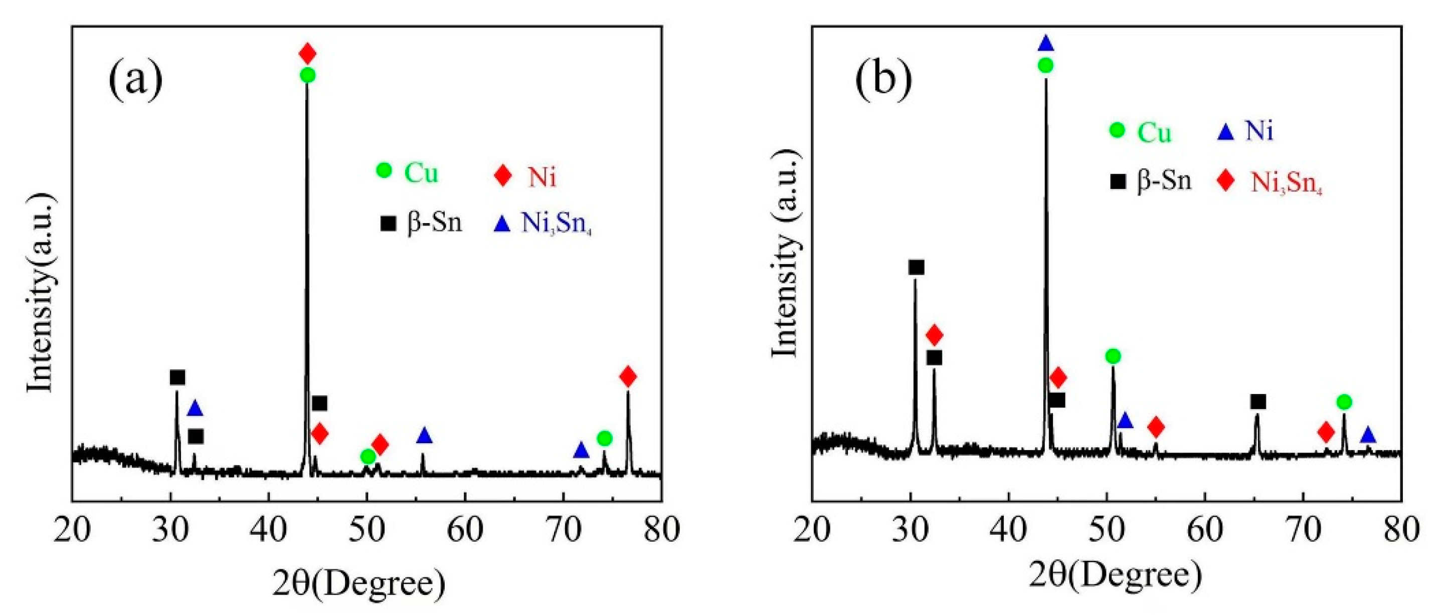
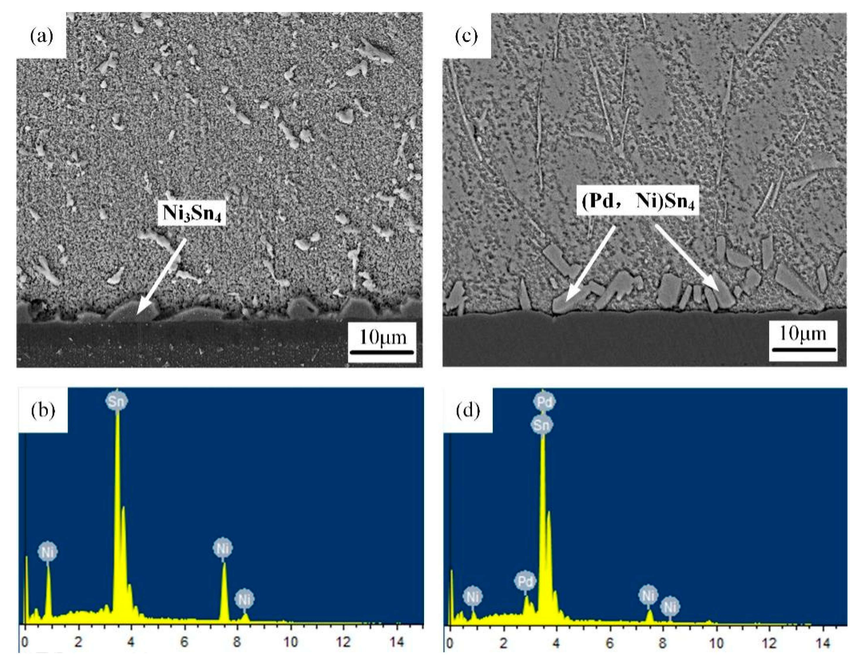
3.1. Original Morphology and Compositions of IMC
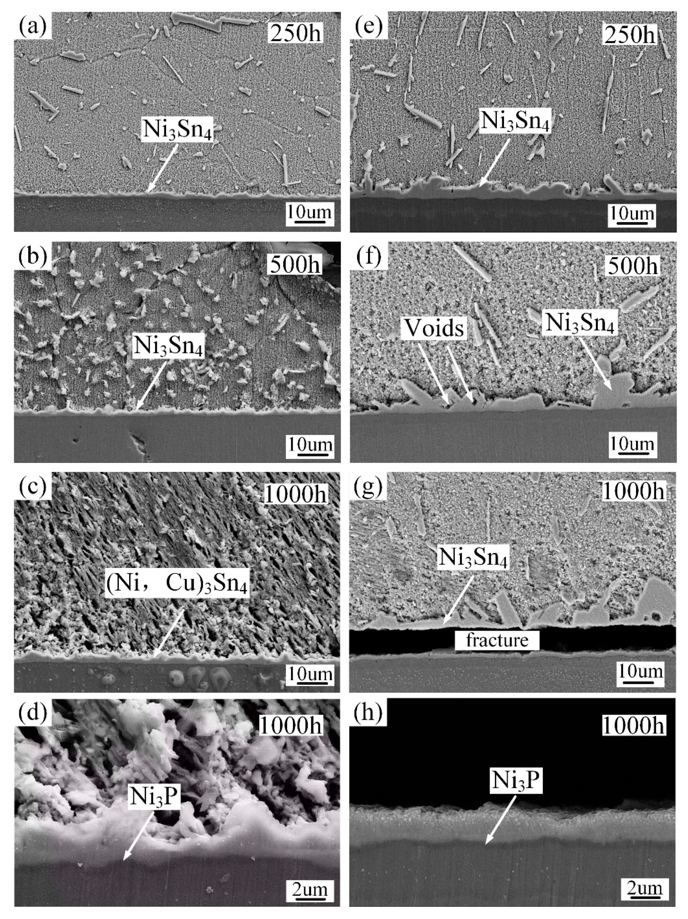
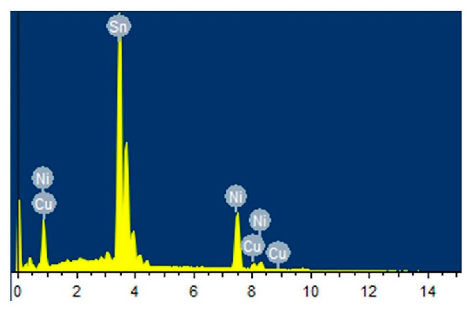
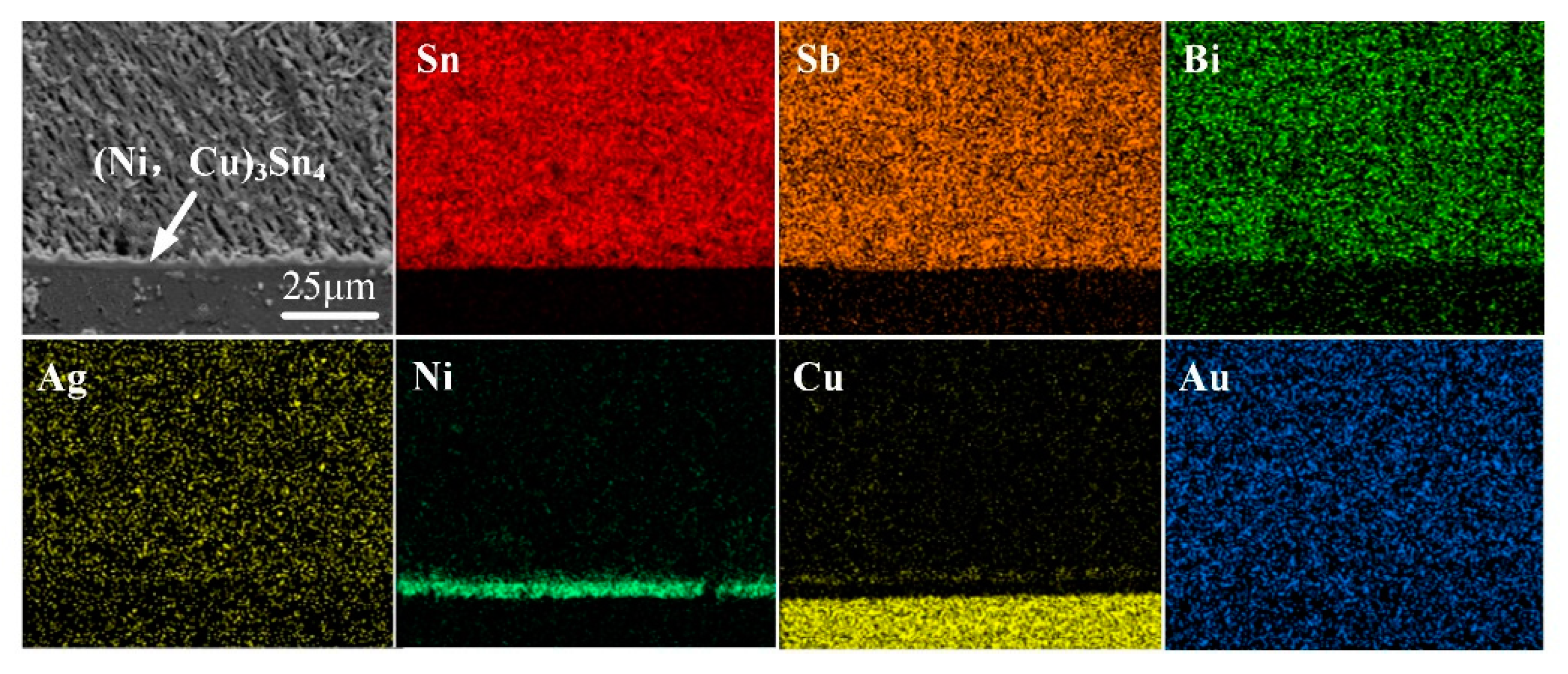
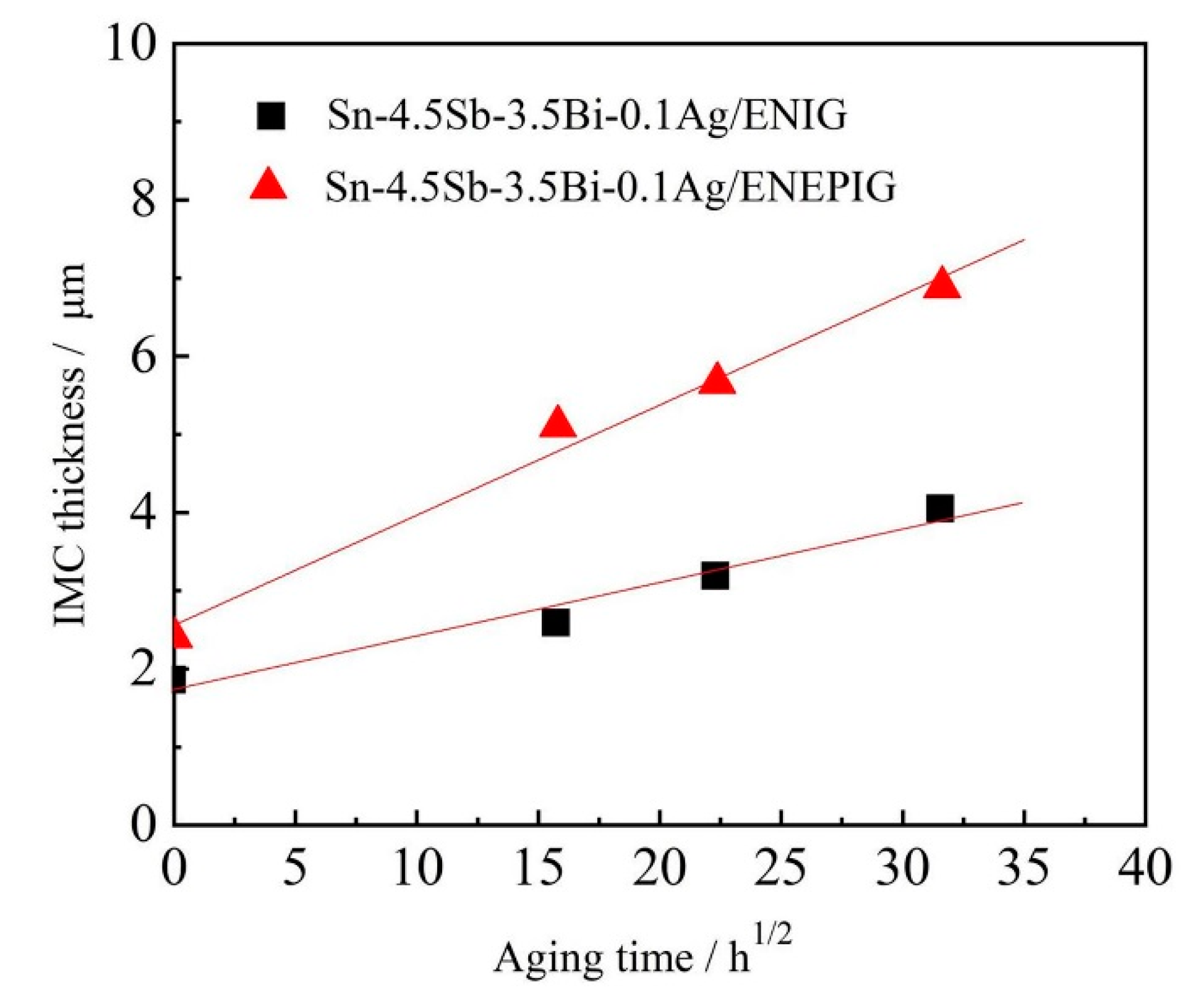
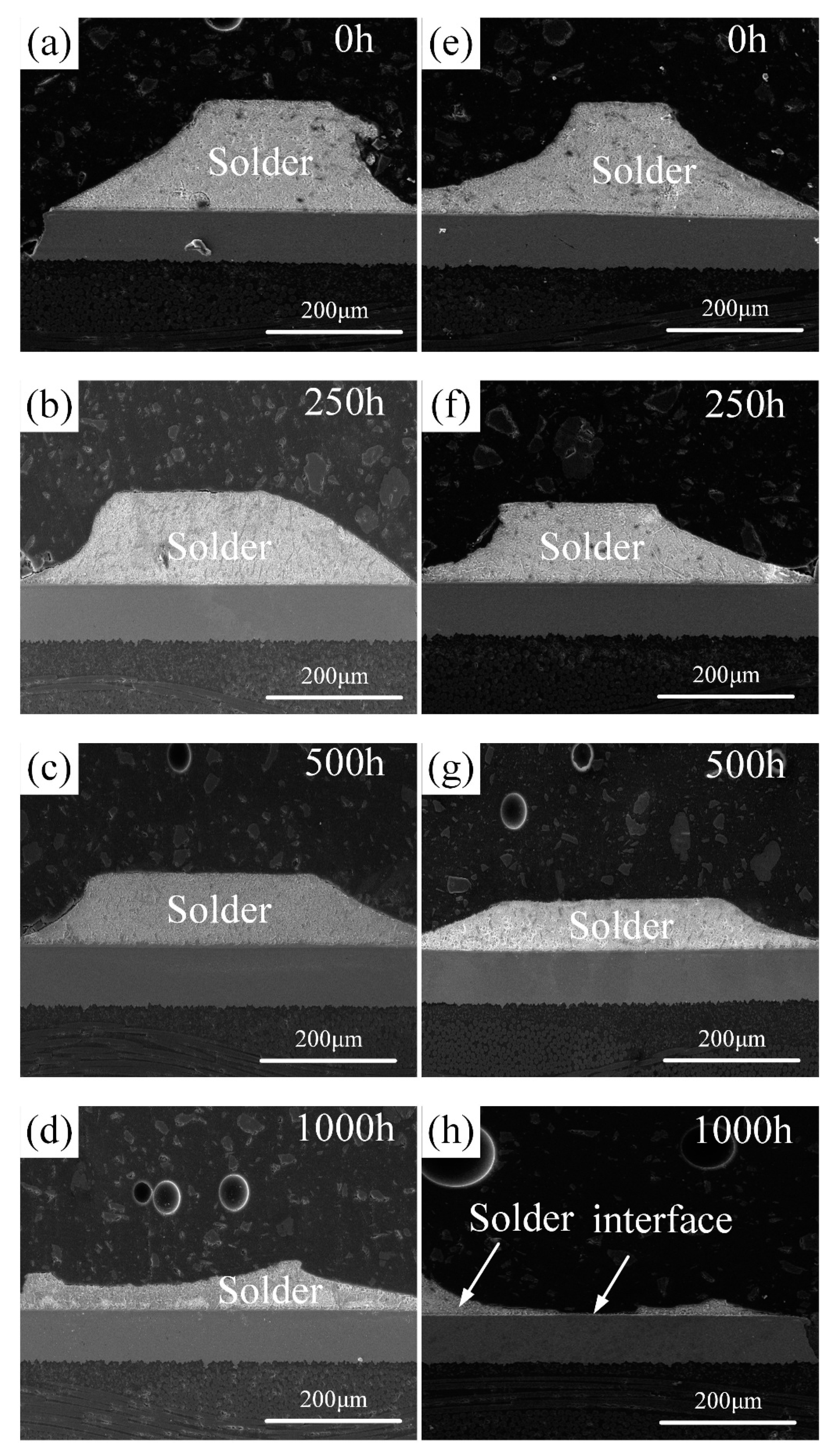
3.2. The Impact of Aging Treatment on IMC
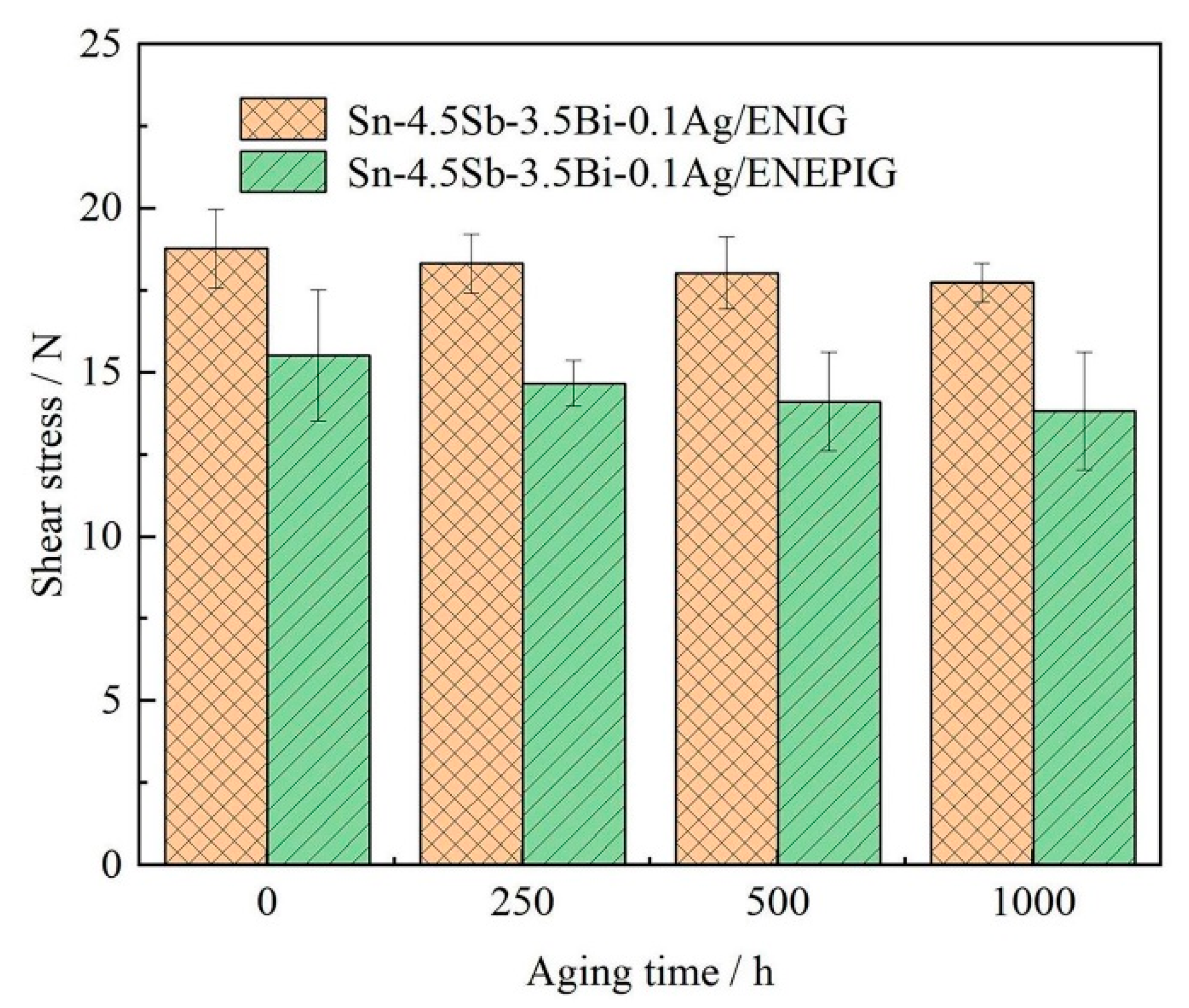
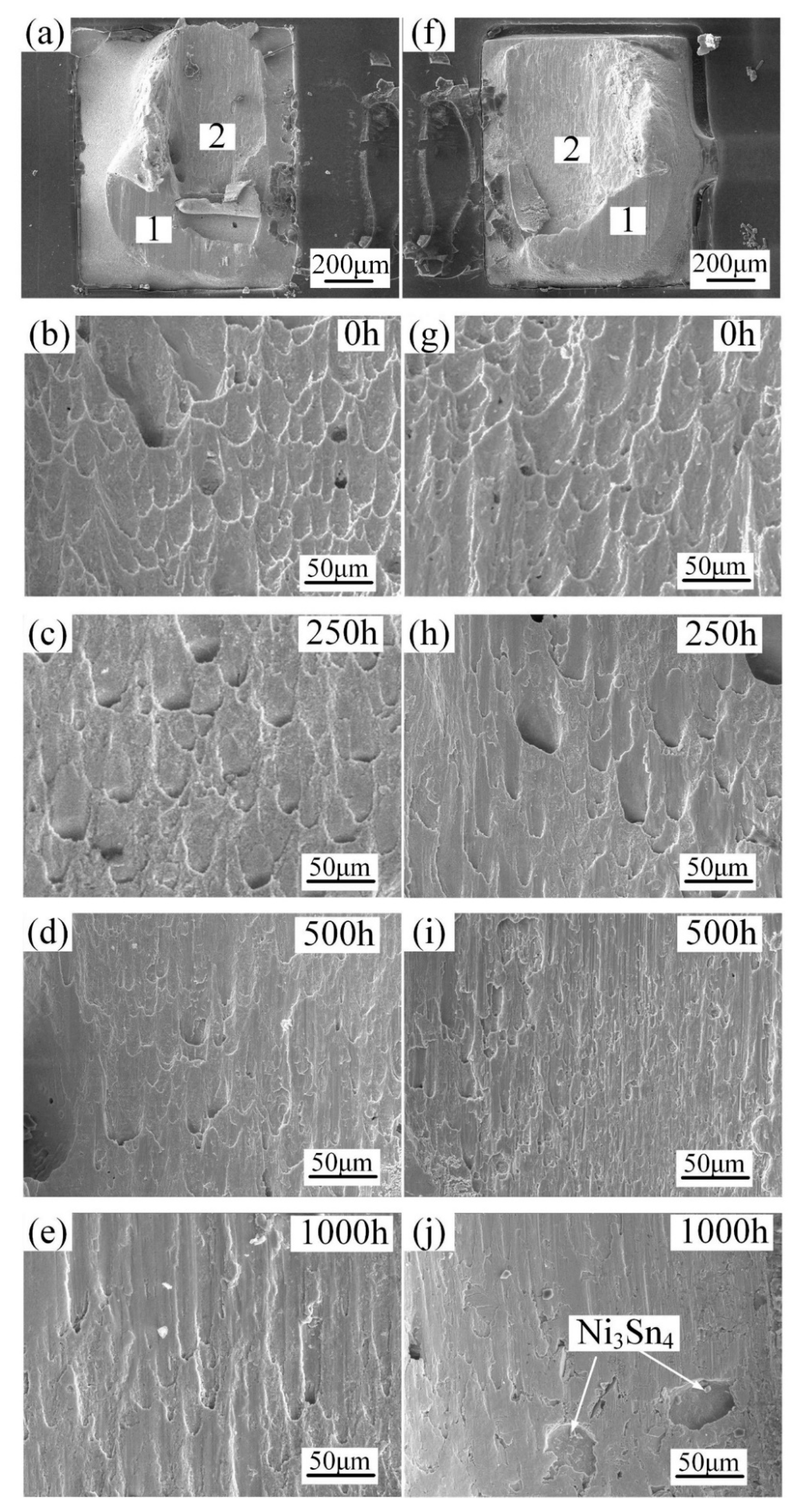
3.3. Mechanical Properties
4. Conclusions
Author Contributions
Funding
Institutional Review Board Statement
Informed Consent Statement
Data Availability Statement
Acknowledgments
Conflicts of Interest
Abbreviations
| ENIG | Electroless Nickel-Immersion Gold |
| ENEPIG | Electroless Nickel-Electroless Palladium-Immersion Gold |
| Sn | Tin |
| Sb | Antimony |
| Bi | Bismuth |
| Ag | Silver |
| Cu | Copper |
| Ni | Nickel |
| Pd | Palladium |
| Au | Gold |
| SEM | Scanning Electron Microscopy |
| EDS | Energy Dispersive X-Ray Spectroscopy |
| XRD | X-ray diffraction |
| IMC | Intermetallic compound |
References
- Puttlitz, K.J.; Stalter, K.A. Handbook of Lead-Free Solder Technology for Microelectronic Assemblies; Marcel Dekker, Inc.: New York, NY, USA, 2004. [Google Scholar]
- Murty, K.L.; Haggag, F.M.; Mahidhara, R.K. Tensile, creep, and ABI tests on sn5%sb solder for mechanical property evaluation. J. Mater. 1997, 26, 839–846. [Google Scholar] [CrossRef]
- McCabe, R.J.; Fine, M.E. Creep of tin, Sb-solution-strengthened tin, and SbSn-precipitate-strengthened tin. Metall. Mater. A 2002, 33, 1531–1539. [Google Scholar] [CrossRef]
- Mahmudi, R.; Geranmayeh, A.R.; Bakherad, M.; Allami, M. Indentation creep study of lead-free Sn-5%Sb solder alloy. Mater. Sci. Eng. A 2007, 457, 173–179. [Google Scholar] [CrossRef]
- Mahmudi, R.; Geranmayeh, A.R.; Rezaee-Bazzaz, A. Impression creep behavior of lead-free Sn-5Sb solder alloy. Mater. Sci. Eng. A 2007, 448, 287–293. [Google Scholar] [CrossRef]
- El-Daly, A.A.; Fawzy, A.; Mohamad, A.Z.; El-Taher, A.M. Microstructural evolution and tensile properties of Sn-5Sb solder alloy containing small amount of Ag and Cu. J. Alloys Compd. 2011, 509, 4574–4582. [Google Scholar] [CrossRef]
- Geranmayeh, A.R.; Nayyeri, G.; Mahmudi, R. Microstructure and impression creep behavior of lead-free Sn-5Sb solder alloy containing Bi and Ag. Mater. Sci. Eng. A 2012, 547, 110–119. [Google Scholar] [CrossRef]
- Duan, N.; Scheer, J.; Bielen, J.; van Kleef, M. The influence of Sn-Cu-Ni(Au) and Sn-Au intermetallic compounds on the solder joint reliability of flip chips on low temperature co-fired ceramic substrates. Microelectron. Reliab. 2003, 43, 1317–1327. [Google Scholar] [CrossRef]
- Zeng, K.; Tu, K.N. Six cases of reliability study of Pb-free solder joints in electronic packaging technology. Mater. Sci. Eng. R 2002, 38, 55–105. [Google Scholar] [CrossRef]
- Foley, J.C.; Gickler, A.; Leprevost, F.H.; Brown, D. Analysis of ring and plug shear strengths for comparison of lead-free solders. J. Mater. 2000, 29, 1258–1263. [Google Scholar] [CrossRef]
- Gong, J.C.; Liu, C.Q.; Conway, P.P.; Silberschmidt, V.V. Evolution of CuSn intermetallics between molten SnAgCu solder and Cu substrate. Acta. Mater. 2008, 56, 4291–4297. [Google Scholar] [CrossRef]
- Wang, F.J.; Yu, Z.S.; Qi, K. Intermetallic compound formation at Sn-3.0Ag-0.5Cu-1.0Zn lead-free solder alloy/Cu interface during as-soldered and as-aged conditions. J. Alloy. Compd. 2007, 438, 110–115. [Google Scholar] [CrossRef]
- Lee, Y.H.; Lee, H.T. Shear strength and interfacial microstructure of Sn-Ag-xNi/Cu single shear lap solder joints. Mater. Sci. Eng. A 2007, 444, 75–83. [Google Scholar] [CrossRef]
- Zhang, R.; Tian, Y.H.; Hang, C.J.; Liu, B.L.; Wang, C.Q. Formation mechanism and orientation of Cu3Sn grains in Cu-Sn intermetallic compound joints. Mater. Lett. 2013, 110, 137–140. [Google Scholar] [CrossRef]
- Sohn, Y.C.; Yu, J. Correlation between chemical reaction and brittle fracture found in electroless Ni(P)/immersion gold–solder interconnection. J. Mater. Res. 2005, 20, 1931–1934. [Google Scholar] [CrossRef]
- Yoon, J.W.; Noh, B.I.; Jung, S.B. Comparison of Interfacial Stability of Pb-Free Solders (Sn-3.5Ag, Sn-3.5Ag-0.7Cu, and Sn-0.7Cu) on ENIG-Plated Cu During Aging. IEEE. Trans. Compon. Packag. Technol. 2010, 33, 64–70. [Google Scholar] [CrossRef]
- Yoon, J.W.; Moon, W.C.; Jung, S.B. Interfacial reaction of ENIG/Sn-Ag-Cu/ENIG sandwich solder joint during isothermal aging. Microelectron. Eng. 2006, 83, 2329–2334. [Google Scholar] [CrossRef]
- Sun, P.; Andersson, C.; Wei, X.C.; Cheng, Z.N.; Shangguan, D.K.; Liu, J. High temperature aging study of intermetallic compound formation of Sn-3.5Ag and Sn-4.0Ag-0.5Cu solders on electroless Ni(P) metallization. J. Alloys Compd. 2006, 425, 191–199. [Google Scholar] [CrossRef]
- Snugovsky, P.; Arrowsmith, P.; Romansky, M. Electroless Ni/Immersion Au interconnects: Investigation of black pad in wire bonds and solder joints. J. Electron. Mater. 2001, 30, 1262–1270. [Google Scholar] [CrossRef]
- Yoon, J.W.; Noh, B.I.; Yoon, J.H.; Kang, H.B.; Jung, S.B. Sequential interfacial intermetallic compound formation of Cu6Sn5 and Ni3Sn4 between Sn-Ag-Cu solder and ENEPIG substrate during a reflow process. J. Alloys Compd. 2011, 509, 153–156. [Google Scholar] [CrossRef]
- Kim, P.G.; Tu, K.N.; Abbott, D.C. Time-and temperature-dependent wetting behavior of eutectic SnPb on Cu leadframes plated with Pd/Ni and Au/Pd/Ni thin films. J. Appl. Phys. 1998, 84, 770–775. [Google Scholar] [CrossRef]
- Tseng, C.F.; Duh, J.G. Correlation between microstructure evolution and mechanical strength in the Sn-3.0Ag-0.5Cu/ENEPIG solder joint. Mater. Sci. Eng. A 2013, 580, 169–174. [Google Scholar] [CrossRef]
- Bader, W.G. Dissolution of Au, Pd, Pt, Cu and Ni in a molten tin-lead solder. Weld. Res. Supp. 1969, 48, 551–557. [Google Scholar]
- Tanaka, S.; Kajihara, M. Kinetics of solid-state reactive diffusion between Sn-Ni alloys and Pd. J. Alloys Compd. 2009, 484, 273–279. [Google Scholar] [CrossRef]
- Baek, Y.H.; Chung, B.M.; Choi, Y.S.; Choi, J.H.; Huh, J.Y. Effects of Ni3Sn4 and (Cu,Ni)6Sn5 intermetallic layers on cross-interaction between Pd and Ni in solder joints. J. Alloys Compd. 2013, 579, 75–81. [Google Scholar] [CrossRef]
- Tseng, C.F.; Lee, T.K.; Ramakrishna, G.; Liu, K.C.; Duh, J.G. Suppressing Ni3Sn4 formation in the Sn–Ag–Cu solder joints with Ni–P/Pd/Au surface finish. Mater. Lett. 2011, 65, 3216–3218. [Google Scholar] [CrossRef]
- Yoon, J.W.; Lee, C.B.; Jung, S.B. Growth of an intermetallic compound layer with Sn-3.5Ag-5Bi on Cu and Ni-P/Cu during aging treatment. J. Electron. Mater. 2003, 32, 1195–1202. [Google Scholar] [CrossRef]
- Cao, L.H.; Chen, Y.B.; Shi, Y.Y. Effects of Alloy Elements on the Interfacial Microstructure and Shear Strength of Sn-Ag-Cu Solder. Acta Metall Sin 2019, 55, 1606–1614. [Google Scholar]
- Ahat, S.; Mei, S.; Le, L. Microstructure and shear strength evolution of SnAg/Cu surface mount solder joint during aging. J. Electron. Mater. 2001, 30, 1317–1322. [Google Scholar] [CrossRef]
- Che, F.X.; Pang, J. Characterization of IMC layer and its effect on thermomechanical fatigue life of Sn-38Ag-0.7Cu solder joints. J. Alloys Compd. 2012, 541, 6–13. [Google Scholar] [CrossRef]


Publisher’s Note: MDPI stays neutral with regard to jurisdictional claims in published maps and institutional affiliations. |
© 2021 by the authors. Licensee MDPI, Basel, Switzerland. This article is an open access article distributed under the terms and conditions of the Creative Commons Attribution (CC BY) license (https://creativecommons.org/licenses/by/4.0/).
Share and Cite
Liang, Z.; Shen, F.; Yang, Z.; Xu, D.; Wei, S.; Peng, Z.; Wang, L.; Wang, D. Effects of Isothermal Aging on Interfacial Microstructure and Shear Properties of Sn-4.5Sb-3.5Bi-0.1Ag Soldering with ENIG and ENEPIG Substrates. Metals 2021, 11, 2027. https://doi.org/10.3390/met11122027
Liang Z, Shen F, Yang Z, Xu D, Wei S, Peng Z, Wang L, Wang D. Effects of Isothermal Aging on Interfacial Microstructure and Shear Properties of Sn-4.5Sb-3.5Bi-0.1Ag Soldering with ENIG and ENEPIG Substrates. Metals. 2021; 11(12):2027. https://doi.org/10.3390/met11122027
Chicago/Turabian StyleLiang, Zhimin, Fei Shen, Zongyuan Yang, Da Xu, Shaowei Wei, Zhenzhen Peng, Liwei Wang, and Dianlong Wang. 2021. "Effects of Isothermal Aging on Interfacial Microstructure and Shear Properties of Sn-4.5Sb-3.5Bi-0.1Ag Soldering with ENIG and ENEPIG Substrates" Metals 11, no. 12: 2027. https://doi.org/10.3390/met11122027
APA StyleLiang, Z., Shen, F., Yang, Z., Xu, D., Wei, S., Peng, Z., Wang, L., & Wang, D. (2021). Effects of Isothermal Aging on Interfacial Microstructure and Shear Properties of Sn-4.5Sb-3.5Bi-0.1Ag Soldering with ENIG and ENEPIG Substrates. Metals, 11(12), 2027. https://doi.org/10.3390/met11122027