Article

Comprehensive Evaluation and Optimization of Level Count for Cascaded H-Bridge Multilevel Inverters with Carrier-Phase-Shifted PWM


by
Zhengxing Li
1,2 and
Jinfeng Li
1,2,3,*
1
School of Interdisciplinary Science, Beijing Institute of Technology, Beijing 100081, China
2
Beijing Key Laboratory of Millimeter Wave and Terahertz Technology, School of Integrated Circuits and Electronics, Beijing Institute of Technology, Beijing 100081, China
3
Department of Electrical and Electronic Engineering, Imperial College London, London SW7 2AZ, UK
*
Author to whom correspondence should be addressed.
Machines 2026, 14(6), 628; https://doi.org/10.3390/machines14060628
Submission received: 7 May 2026 / Revised: 27 May 2026 / Accepted: 28 May 2026 / Published: 1 June 2026
(This article belongs to the Special Issue Power Converters: Topology, Control, Reliability, and Applications)

Abstract

Cascaded H-bridge (CHB) multilevel inverters are pivotal in high-power applications, such as renewable energy subsystems and motor drives, due to their superior modularity and harmonic performance. However, selecting the optimal number of levels remains a complex engineering trade-off between power quality, switching losses, and system complexity. This study presents a systematic investigation into CHB inverters ranging from three to twenty-one levels under carrier-phase-shifted sinusoidal pulse width modulation (CPS-SPWM) control. A detailed MATLAB/Simulink framework in version R2023a was established, incorporating a zero-order hold (ZOH) data synchronization protocol and parameterized macro-model MOSFETs to accurately quantify total harmonic distortion (THD) and individual switching energy dissipation. To evaluate the efficiency–quality equilibrium, a novel comprehensive evaluation index, the performance-to-loss ratio (PLR), is proposed. Simulation results indicate that while THD improves significantly with higher level counts, the marginal gains diminish beyond the 13-level configuration. Utilizing the PLR framework, the nine-level configuration is identified as a local optimum for cost-sensitive modularity, whereas the twenty-one-level setup provides the global optimum for high-performance scenarios where spectral purity is paramount. Accordingly, this proof-of-concept study provides a quantitative roadmap for designers and experimentalists to navigate the complex design space of multilevel inverters, enabling optimal allocation of hardware resources toward the net-zero vision while guiding future experimental efforts away from costly, exhaustive hardware characterization.

1. Introduction

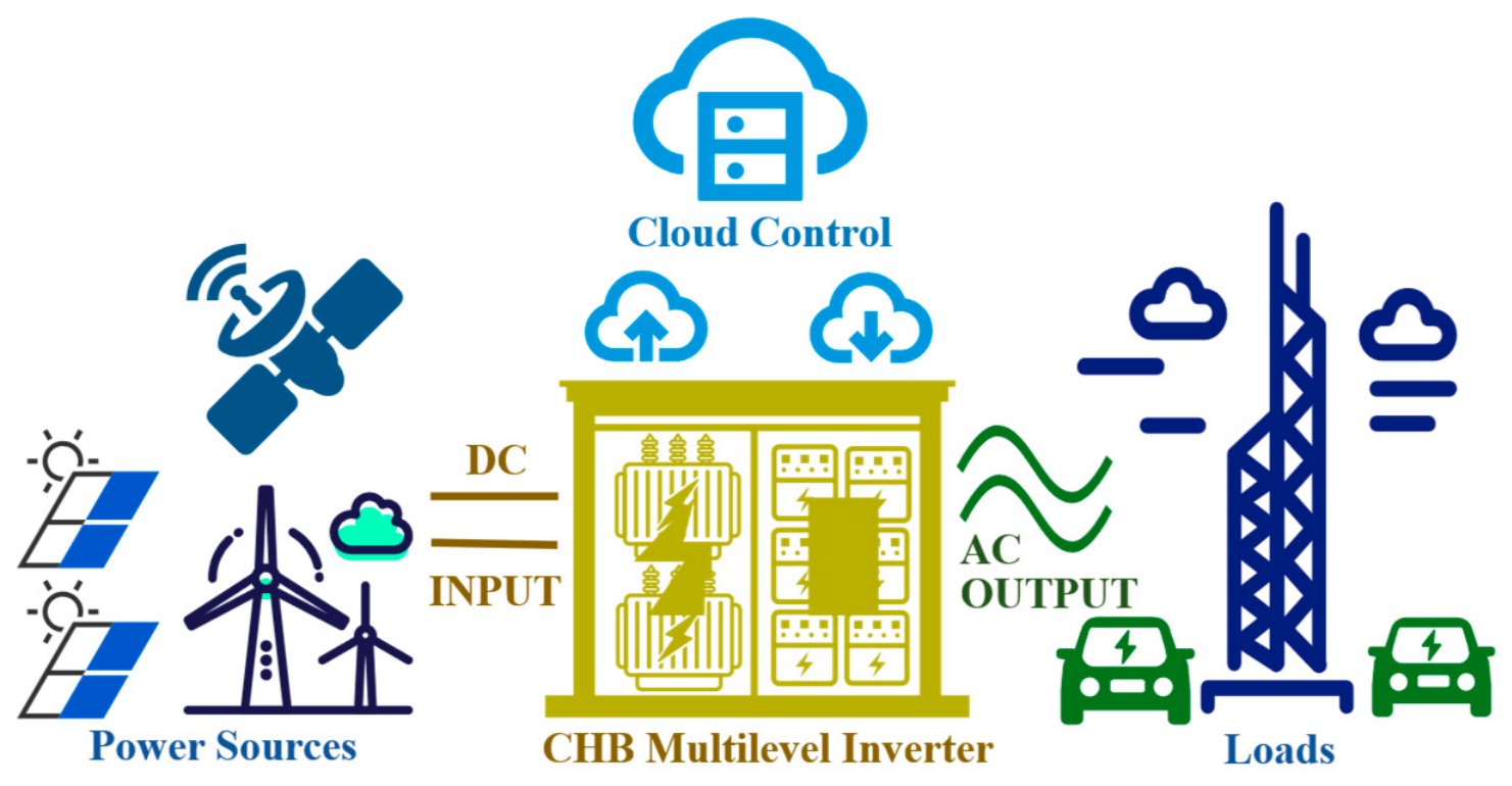
Power electronics [1,2,3,4] establishes a fundamental link between electrical and electronic engineering, specifically within the domain of switching techniques [5,6,7], encompassing both hardware architectures [8,9,10] and control methodologies [11,12]. Instead of employing dissipative linear methods, such as resistive regulation, to manage power flow, modern power electronics utilizes semiconductor switches (e.g., MOSFETs [13] and IGBTs [14]) to turn power on and off at high frequencies. Built upon this foundational switching paradigm and driven by the global imperative of carbon neutrality, multilevel inverters (MLIs) [15] have become pivotal in modern medium-to-high voltage power electronic systems. As macro-architectures of energy networks evolve toward cloud-edge-device collaborative paradigms [16], MLIs serve as the critical energy routing hubs. As conceptualized in Figure 1, they play an indispensable role in bridging decentralized DC sources—such as grid-connected renewable energy subsystems (solar photovoltaics and wind power [17]) and aerospace DC buses—with dynamic AC loads, including advanced motor drives [18] and electric vehicle (EV) propulsion systems [19,20].
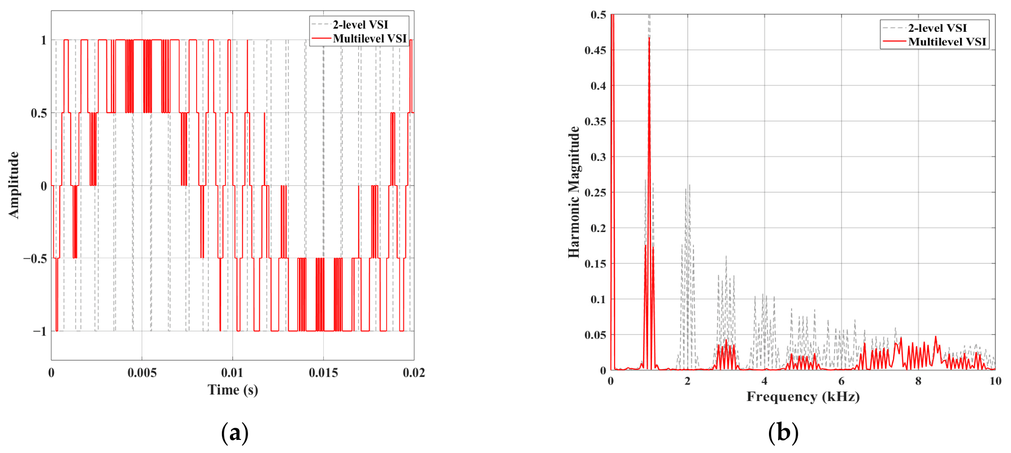
Compared to conventional two-level inverters [21], MLIs synthesize a staircase output voltage waveform by combining multiple lower DC voltage levels. This fundamental structural shift provides significant advantages. As comparatively illustrated in Figure 2a, the conventional two-level topology subjects the semiconductor switches to the full DC-link voltage, resulting in extremely steep d v / d t gradients during switching transitions. This severe d v / d t stress accelerates the degradation of motor winding insulation and introduces significant common-mode currents [22]. By contrast, the refined staircase waveform of MLIs drastically reduces the voltage step size ( V ), which fundamentally suppresses the d v / d t stress. Consequently, this yields a substantial reduction in high-frequency electromagnetic interference (EMI) emissions (Figure 2b) and superior total harmonic distortion (THD) profiles, while eliminating the need for bulky, expensive step-up transformers or heavy passive filters. These inherently translate to lower cost and reduced footprint, guiding the power electronics industry toward sustainability.
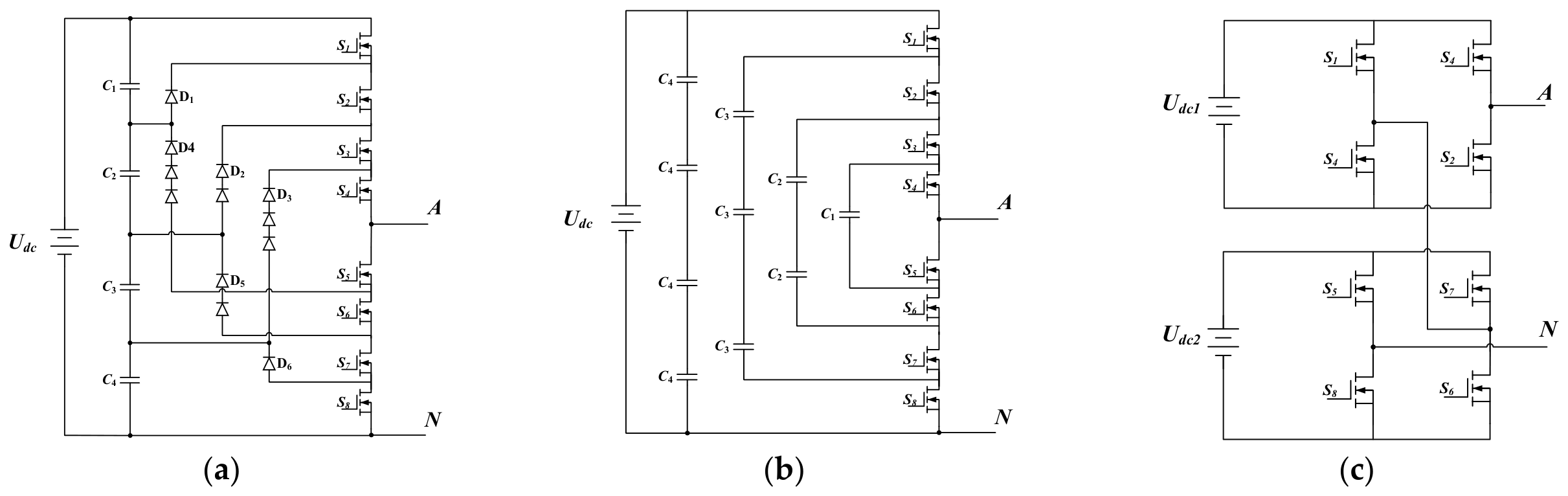
To physically realize these high-resolution multilevel waveforms, various topologies have been proposed. Figure 3 presents a structural comparison of the three classic MLI architectures. The neutral point clamped (NPC) [23,24] and flying capacitor (FC) [25] topologies rely on passive components (clamping diodes and flying capacitors, respectively) to synthesize intermediate voltage levels. However, as the required number of levels increases, these topologies suffer from exponential growth in hardware complexity and severe capacitor voltage balancing challenges. Among them, the cascaded H-Bridge (CHB) topology [26,27] stands out due to its exceptional modularity, high reliability, and linear scalability. By utilizing completely independent DC sources, CHB inverters entirely bypass the voltage balancing bottlenecks inherent in NPC and FC topologies. To effectively drive the metal-oxide-semiconductor field-effect transistors (MOSFETs) within the CHB architecture, carrier-phase-shifted sinusoidal pulse width modulation (CPS-SPWM) [28,29] is widely adopted as a core control strategy. By comparing a single modulating wave with multiple phase-shifted triangular carriers, CPS-SPWM effectively multiplies the equivalent output switching frequency, thereby significantly improving harmonic performance [30] without compromising the energy efficiency of individual MOSFETs.
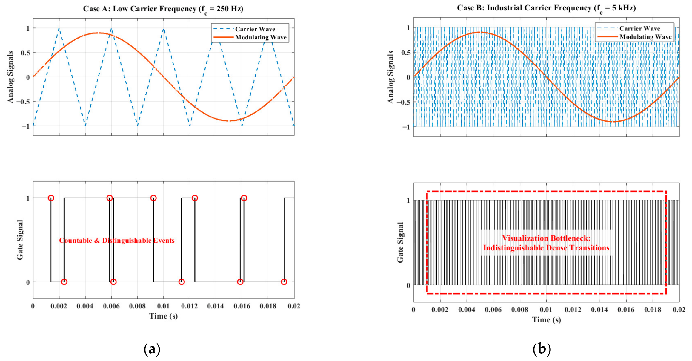
Despite the well-documented advantages [31,32] of CHB inverters and CPS-SPWM, one of the critical unanswered questions in the field remains the optimum number of levels for practical industrial deployment. While increasing the level count monotonically improves the output power quality and decentralizes the thermal stress per cell, it simultaneously necessitates a linear increase in the number of active components and gate-drive isolation circuits. This escalating structural complexity [33] inherently amplifies the cumulative switching losses and introduces potential hardware failure points. Furthermore, accurately quantifying these switching losses—a prerequisite for solving this optimum-level puzzle and achieving reliable thermal management—is severely hindered by the “visualization bottleneck”. As visually demonstrated in Figure 4, when the carrier frequency is relatively low, switching events are clearly distinguishable. However, as the carrier frequency increases to industrially relevant high frequencies (e.g., above 1 kHz), traditional timing diagrams become extremely dense blocks of ink. This makes it impossible to reliably identify individual switching transitions by manual or visual inspection, severely hindering precise switching count statistics and loss calculations. Conventional evaluation methods typically isolate THD or switching loss, failing to capture the holistic “system-level trade-off” required for modern cost-sensitive and high-performance applications.
To bridge these research gaps, this study presents a comprehensive evaluation and optimization framework for CHB multilevel inverters ranging from 3 to 21 levels. The upper bound of 21 levels (i.e., cascading 10 H-bridge units per phase) is selected as a proof-of-concept ceiling, capturing the transition from diminishing returns in harmonic performance to escalating hardware complexity beyond this point. Given that experimental characterization of switching losses across multiple level configurations is technically demanding, time-consuming, and costly, this work introduces a simulation-driven framework that directly informs future experimental design. The main contributions of this paper are summarized as follows:
(1) A universal MOSFET switching count mathematical model under CPS-SPWM is derived and empirically validated through a novel proportional-scaling simulation methodology, effectively bypassing the high-frequency observability bottleneck.
(2) A detailed MATLAB/Simulink framework, incorporating non-ideal parameterized macro-models and a zero-order hold (ZOH) data synchronization protocol, is established to precisely quantify THD and individual transient switching energy dissipation across different level configurations.
(3) A multidimensional evaluation index, the performance-to-loss ratio (PLR), is proposed to mathematically penalize both harmonic distortion and hardware complexity. By applying the PLR framework, this research quantitatively identifies the nine-level configuration as a local optimum for economical modularity, and the twenty-one-level configuration as the global optimum for maximum spectral purity, providing a robust quantitative roadmap for the next generation of power converters.
Importantly, the proposed PLR-driven framework is not limited to simulation. By explicitly identifying which level configurations yield optimal trade-offs between performance and hardware complexity, it enables experimentalists to focus their efforts on the most promising candidates (e.g., nine-level for economical designs, twenty-one-level for high-performance applications). This targeted approach bypasses the need for exhaustive experimental characterization of every possible level count—a process that is often impractical due to the high cost and technical difficulty of accurately measuring transient switching losses in multilevel inverters.

2. Materials and Methods

2.1. Theoretical Paradigms of CHB Multilevel Inverters and Boundary Condition Preservation

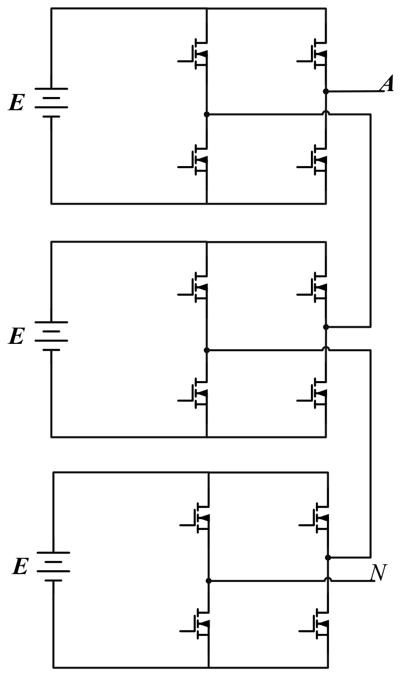
The cascaded H-Bridge (CHB) topology offers a modular alternative to traditional multilevel architectures by employing independent DC sources (as illustrated in Figure 5 for a representative 7-level configuration), achieving a linear scaling relationship with superior ease of control. From a mathematical perspective, the total output phase voltage U a b of an N -cell cascaded inverter is the sum of the individual cell outputs. For a single-phase system with N cascaded units, each cell provides three discrete voltage levels ( + E ,   0 ,   E ). Consequently, the maximum output voltage is N E , and the total number of phase voltage levels ( L p h a s e ) and the maximum possible number of distinct line-to-line voltage levels ( L l i n e ) in a star (Y) configuration are determined by (1) and (2), respectively:
L p h a s e = 2 N + 1 ,
L l i n e = 4 N + 1 .
To derive a scientifically valid comparison across different level counts (ranging from 3 to 21 levels), it is imperative to isolate the effect of the “level count” from the voltage magnitude. Therefore, a rigorous “Boundary Condition Preservation via DC-Link Scaling” protocol is implemented in this study. As the number of cascaded H-bridge cells ( N ) increases, the DC-link voltage assigned to each individual cell ( U d c _ c e l l ) is inversely scaled following the relationship U d c _ c e l l = U p e a k / N . The detailed scaling configurations for all investigated topologies are systematically tabulated in Table 1. This systematic adjustment ensures that the maximum output phase voltage remains fixed at a nominal 240 V regardless of the topology’s complexity, allowing subsequent performance and loss analyses to reflect the intrinsic characteristics of the multilevel architecture rather than artifacts of varying voltage stress.

2.2. CPS-SPWM Control and Switching Count Mathematical Modeling

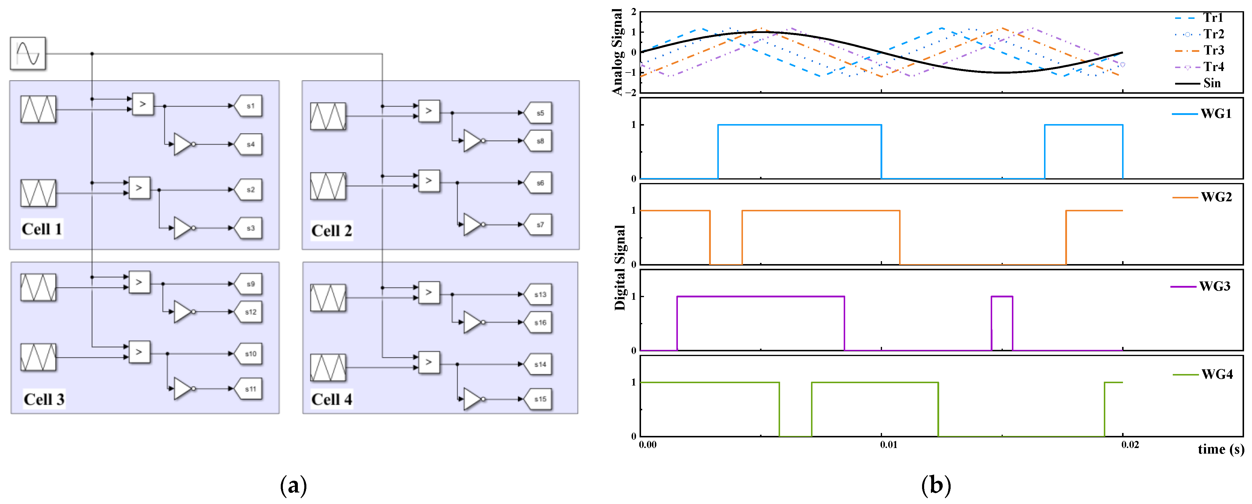
To effectively drive the MOSFETs within the CHB array, the carrier-phase-shifted sinusoidal pulse width modulation (CPS-SPWM) strategy is adopted. In this mechanism (exemplified by the 9-level control logic in Figure 6a), all H-bridge cells share the same sinusoidal modulating wave but utilize triangular carriers that are phase-shifted by a specific angle. For an N -cell system using unipolar modulation, the phase shift θ between adjacent carriers is θ = π / N . This coordinated phase-shifting facilitates an equivalent output switching frequency of 2 N f c (where f c is the carrier frequency), significantly improving the harmonic performance without increasing the switching stress on individual MOSFETs.
Furthermore, accurately quantifying the switching events is critical for evaluating the thermal dissipation of the inverter. Under the CPS-SPWM paradigm, the triangular carrier intersects the modulating wave twice per period, resulting in one turn-on and one turn-off event per carrier cycle (as visually demonstrated in the timing diagram in Figure 6b). Given the carrier frequency ( f c ) and the modulation frequency ( f m ), the theoretical number of switching events for a single MOSFET per modulation cycle ( N s w i t c h ) is formulated as (3):
N s w i t c h = 2 × f c f m .
This universal formula proves that the phase-shifting manipulation only redistributes the switching events uniformly in the time domain without altering the total count per component. To overcome the “visualization bottleneck” at high frequencies (e.g., f c = 1 kHz), a “Proportional Scaling Methodology” was employed in our preliminary validation. By executing a dedicated simulation benchmark at a reduced carrier frequency ( f c = 100 Hz) while maintaining f m = 50 Hz (which corresponds to the exact waveforms plotted in Figure 6b), the manual count yielded exactly 4 events per cycle, achieving a 0% deviation from the theoretical prediction and thereby verifying the accuracy of (3).

2.3. Detailed Simulation Infrastructure and Data Synchronization

To bridge the gap between idealized circuit theory and practical engineering, a detailed physical-layer simulation framework was constructed using the MATLAB/Simulink Simscape Electrical library. The MOSFET components were implemented using parameterized macro-models, meticulously calibrated to account for non-ideal conduction characteristics, including the field-effect on-resistance ( R o n ) and the non-linear response of internal anti-parallel diodes. To validate the trustworthiness of these macro-models, the simulated switching loss characteristics were cross-referenced with the experimental data of equivalent MOSFETs documented in the existing literature. To ensure numerical convergence across the 10 cascaded cells in the 21-level model, a fixed-step solver (ode3, Bogacki–Shampine) was utilized with a fundamental sample time of 1   μ s, providing a 1000-fold oversampling of the 1 kHz carrier signal.
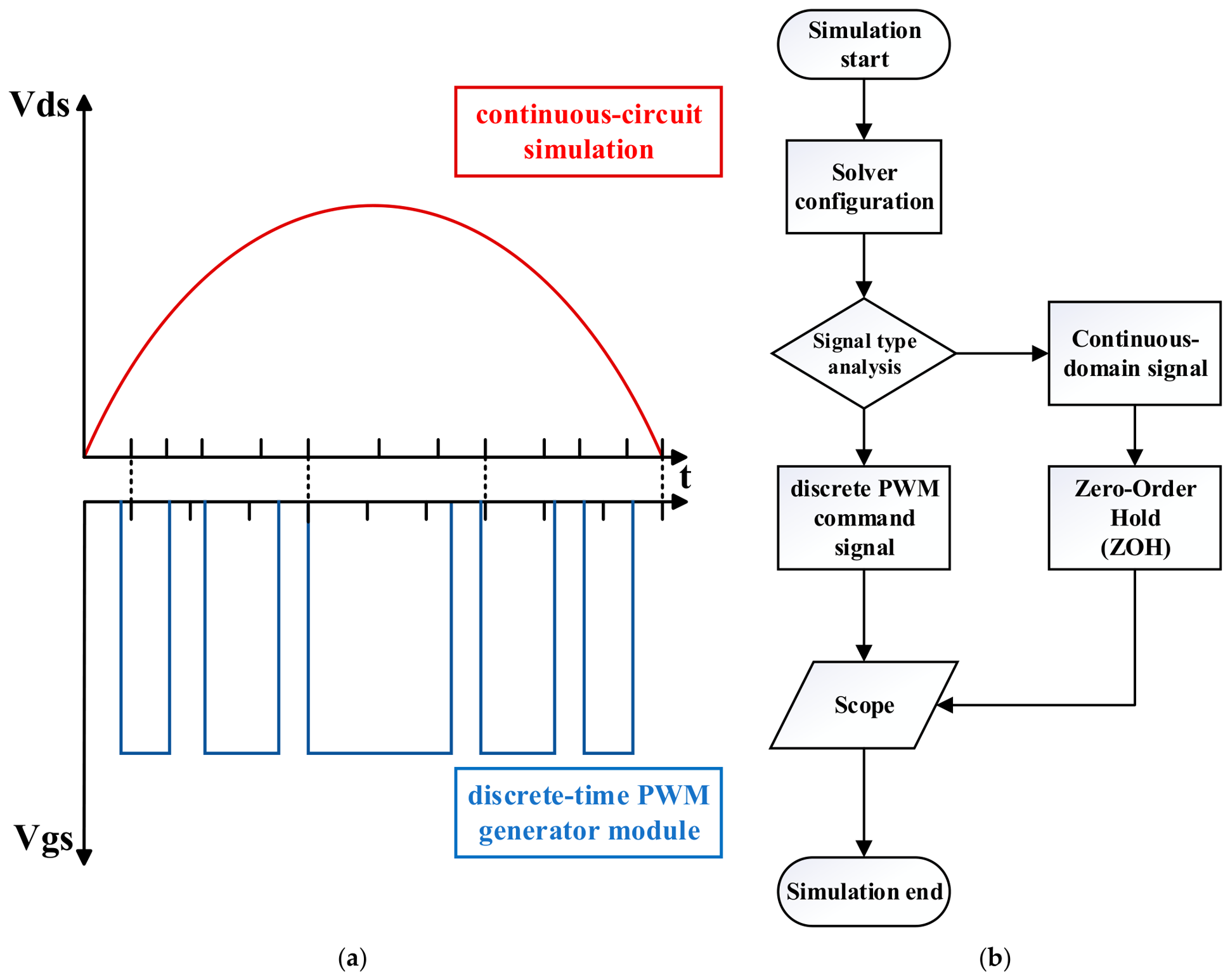
A sophisticated challenge in power electronic modeling involves the interaction between the discrete-time PWM control domain and the continuous-time physical power stage. Preliminary tests identified a critical “sampling density mismatch” (as graphically illustrated in Figure 7a), which prevented the accurate element-wise multiplication required for instantaneous power calculation ( P = V d s · I d ) and subsequent transient energy integration. To remediate this vulnerability, a specialized data synchronization protocol was established utilizing zero-order hold (ZOH) blocks (see the operational flowchart in Figure 7b).
The ZOH strategy serves as a temporal bridge, effectively freezing the discrete control signals at the 1   μ s sampling intervals to align perfectly with the continuous-time feedback from the physical sensors. This methodology ensures that the switching energy dissipation integration is based on mathematically aligned data arrays, providing the precision necessary to evaluate marginal efficiency changes as the level count scales from 3 to 21 in this proof-of-concept study.

3. Results and Analysis

3.1. Detailed Waveform Synthesis and Harmonic Characterization

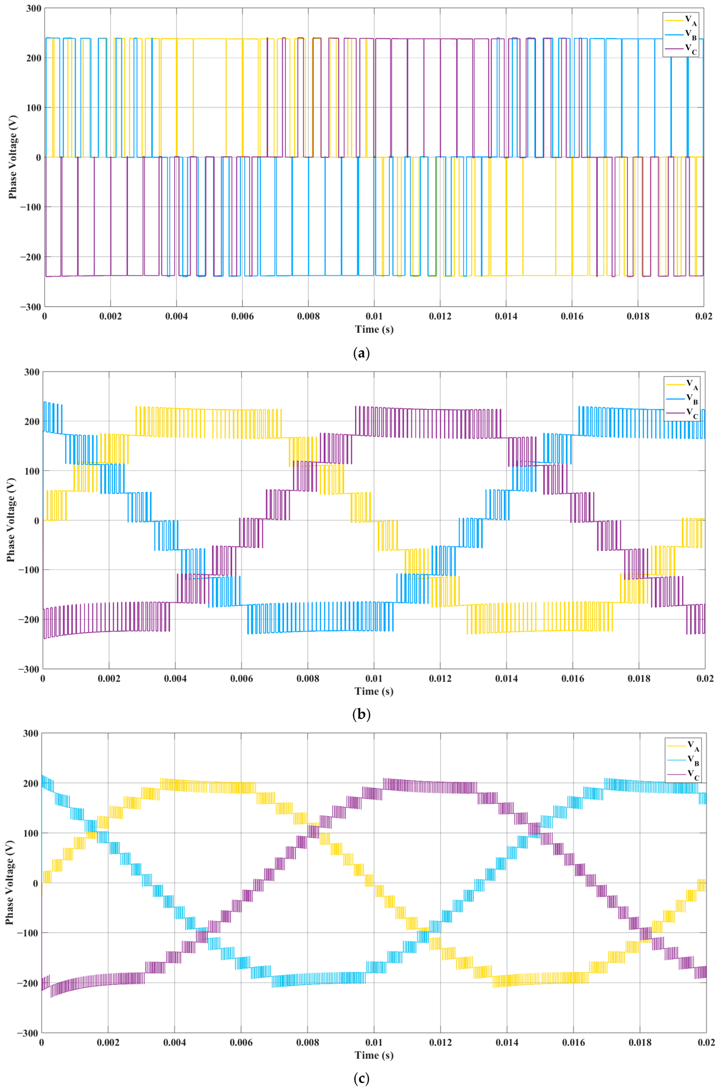
The empirical validation of the modular expansion protocol begins with the synthesis of output waveforms. A comprehensive sequence of simulations was conducted to capture the phase voltage and current profiles for configurations ranging from three to twenty-one levels. As the level count scales up, a clear “staircase refinement” trend is observable (as depicted in Figure 8 for representative three-level, nine-level, and twenty-one-level configurations). While the baseline three-level waveform exhibits pronounced discrete voltage steps, the twenty-one-level output achieves a near-sinusoidal profile even before the application of any inductive filtering. This progressive refinement significantly reduces the d v / d t stress on the load, serving as the primary justification for adopting higher-level architectures.
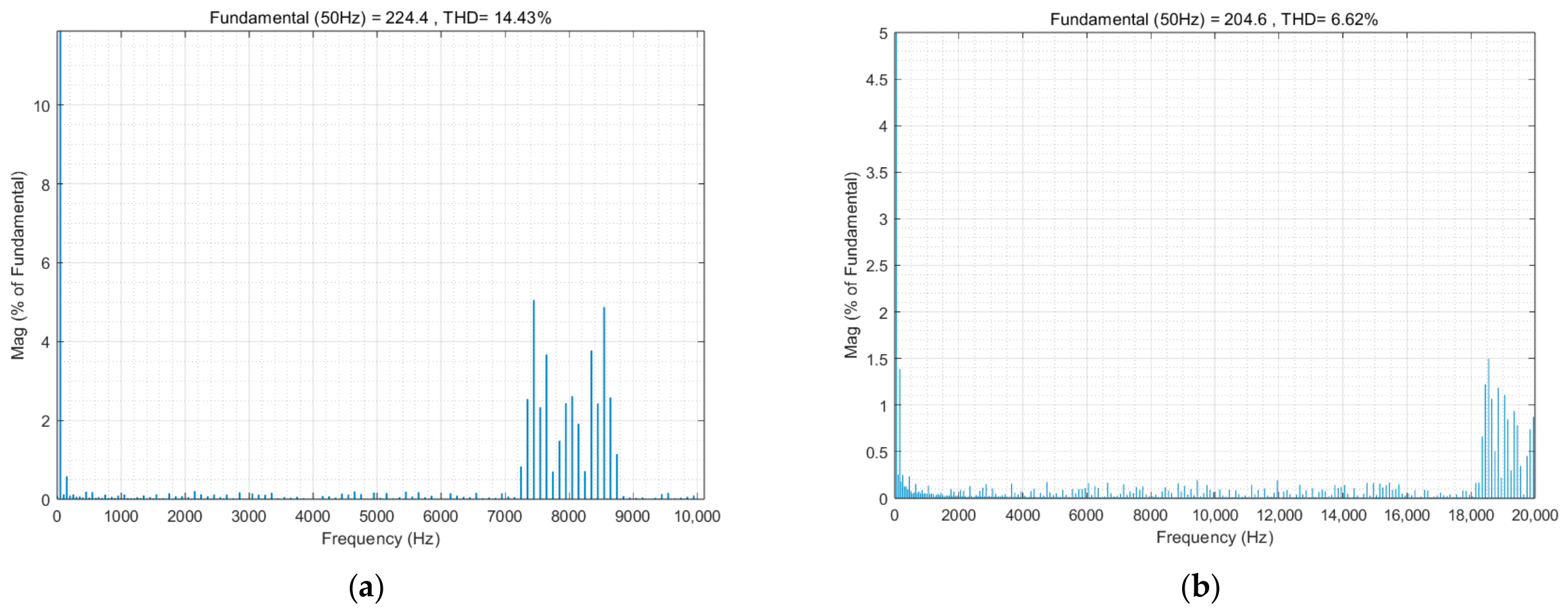
Beyond time-domain improvements, the spectral integrity of the CHB inverter was evaluated using fast Fourier transform (FFT) analysis. In accordance with the frequency multiplication theory of the CPS-SPWM strategy, the dominant harmonic clusters are strategically shifted toward the high-frequency sidebands centered around 2 N f c (see Figure 9). For instance, in the nine-level system ( N = 4), the dominant cluster appears around 8 kHz. Similarly, in the twenty-one-level system ( N = 10) with a 1 kHz carrier, the primary harmonic noise is pushed to the vicinity of 20 kHz. This “spectral shifting” phenomenon leaves the low-frequency range near the 50 Hz fundamental remarkably clean, thereby drastically relaxing the size and cost requirements for output LC filters in grid-tied applications.
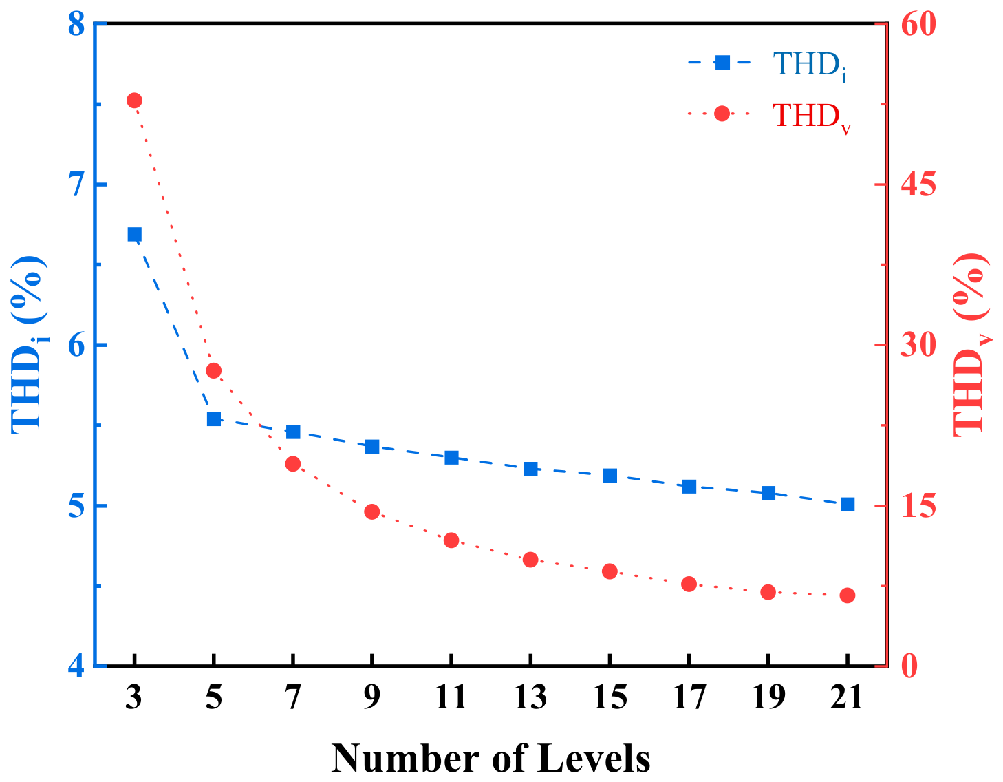
Quantitatively, the relationship between the number of levels and the total harmonic distortion (THD) demonstrates a robust inverse correlation. As the level count increases from three to twenty-one, the voltage THD drops dramatically from 52.83% to 6.62% (illustrated in Figure 10). However, a critical non-linear asymptotic behavior is observed: the marginal gain in THD reduction becomes notably shallower beyond the 13-level mark. This diminishing return suggests that simply maximizing the level count for improved power quality may eventually be outweighed by the escalating system complexity.

3.2. Microscopic Assessment of Intra-Cell Switching Energy

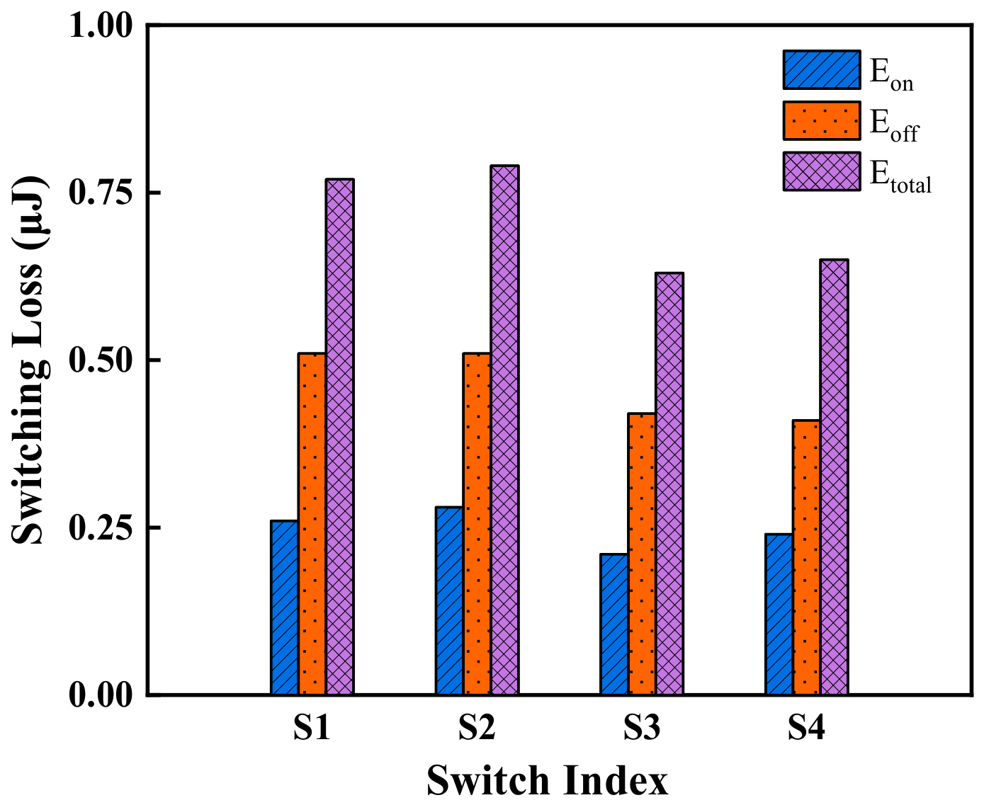
While macroscopic power quality improves with modular expansion, evaluating the localized thermal stress on individual semiconductor devices is equally vital for system reliability. Utilizing the established precise integration windows, the transient energy dissipation during turn-on ( E o n ) and turn-off ( E o f f ) transitions was captured. A microscopic breakdown of the switching losses for the four transistors ( S 1 S 4 ) within the first H-bridge unit (Cell 1) of the nine-level inverter is presented in Figure 11.
A critical physical insight derived from these measurements is that the turn-off energy dissipation consistently exceeds the turn-on energy across all components, typically accounting for over 60% of the total switching loss. This discrepancy is attributed to the inherent capacitance and current-tailing effects during the MOSFET’s transition from a saturated to a cutoff state. Furthermore, the total loss distribution is shown to be non-uniform within the cell. Under balanced load conditions, S 1 and S 2 handle a slightly higher proportion of the switching losses compared to S 3 and S 4 . This intra-cell asymmetry highlights the necessity for component-specific thermal management strategies, particularly in space power applications where convective cooling is unavailable.

3.3. Macroscopic Scaling Effects on Total Power Dissipation

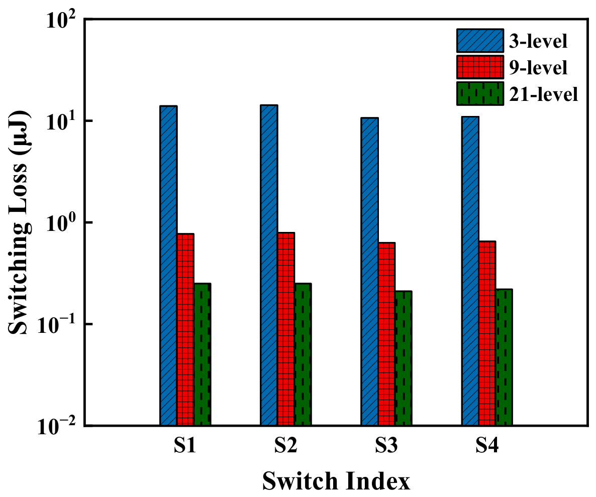
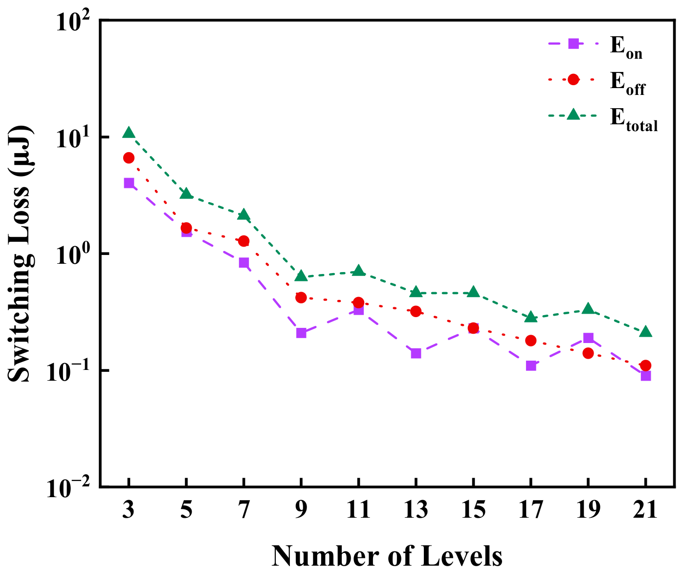
The implementation of the DC-link scaling protocol yields a profound impact on the switching energy dissipation. The evolution of switching losses as a function of level count is quantified in Table 2. A direct comparison (Figure 12) reveals a drastic, significant reduction in per-component switching energy as the topology scales up. Specifically, the total switching energy per event plummets from 10.66 μ J in the three-level baseline to 0.63 μ J in the nine-level configuration, and further down to a mere 0.21 μ J in the twenty-one-level case. This exceptional reduction is a direct consequence of the decentralized voltage stress, where each module in the 21-level system handles only a fraction (24 V) of the 240 V peak voltage.
However, a broader examination across the three to twenty-one level spectrum (plotted using a semi-logarithmic scale in Figure 13) reveals a complex trade-off. While the per-device switching losses decline monotonically from three to eleven levels, the absolute changes become extremely subtle and exhibit minor asymptotic fluctuations beyond the thirteen-level mark. Crucially, although the individual transistor efficiency is maximized in higher-level configurations, this benefit must be balanced against the cumulative loss penalty. For instance, the 21-level system employs 120 MOSFETs across three phases, resulting in a linear accumulation of baseline conduction losses and gate-drive power consumption. This contradiction between individual thermal relief and system-level structural penalty strictly limits the blind pursuit of higher-level counts.
It should be noted that this study primarily evaluates transient switching losses. In practical deployments, the total system efficiency will be further degraded by conduction losses, gate-driver power consumption, and dead-time effects. For high-level configurations such as the 21-level inverter (employing 120 MOSFETs), the linear accumulation of gate-driver losses will significantly amplify the total power dissipation, further justifying the necessity of penalizing the component count ( N ) in the evaluation metric.

4. Discussions and Outlook

4.1. The Engineering Dilemma: Power Quality vs. Hardware Complexity

The empirical results presented in Section 3 highlight a fundamental engineering conflict in the design of CHB multilevel inverters: the simultaneous pursuit of high power quality and high system efficiency. As the level count scales from three to twenty-one, a monotonic reduction in THD is achieved, accompanied by a significant decrease in individual MOSFET switching losses due to the decentralized voltage stress. However, these benefits are counterbalanced by the “law of diminishing marginal returns”. Beyond the 13-level configuration, the gradient of improvement in THD becomes notably shallower. Concurrently, the system necessitates a linear increase in the number of active components (e.g., 40 MOSFETs per phase for a 21-level setup) and their associated gate-drive isolation complexities. Conventional evaluation methods that isolate THD or switching loss individually fail to capture this holistic system-level trade-off, making it strategically imperative to establish a unified metric that penalizes both harmonic distortion and hardware redundancy.

4.2. Formulation of the Performance-to-Loss Ratio (PLR) Framework

To bridge the gap between idealized simulation results and practical industrial decision-making, this research proposes the performance-to-loss ratio (PLR) as a comprehensive multidimensional figure-of-merit. Unlike standard efficiency metrics, the PLR integrates power quality (THD), thermal stress (individual switching power loss, P l o s s ), and structural complexity (total component count, N ) into a single optimization objective. The indices for current ( P L R i ) and voltage ( P L R v ) are formulated as (4) and (5), respectively:
P L R i = 1 ( T H D i ) α × ( P l o s s ) β × N γ   W 1 ,
P L R v = 1 ( T H D v ) α × ( P l o s s ) β × N γ   W 1 .
where α ,   β , and γ are empirical weighting factors representing the relative importance of power quality, thermal management, and system cost/complexity, respectively. In our baseline analysis, equal weights ( α = β = γ = 1 ) are assumed to establish a generalized framework.
In these expressions, the product in the denominator represents the composite system penalty. As the level count increases, the rapid decline in P l o s s and T H D must outpace the linear growth of N for the PLR to show an upward trend. The inclusion of N as a primary variable ensures that the index mathematically accounts for the heightened failure rate, procurement costs, and control latency associated with adding H-bridge cells.

4.3. Identification of Optimal Level Nodes: Local vs. Global Optima

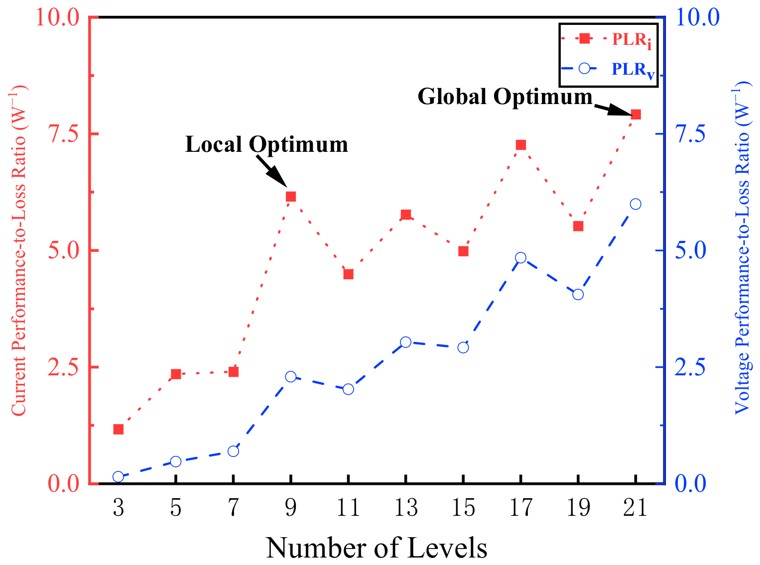
The empirical evaluation of the PLR indices across the 3 to 21 level spectrum reveals a distinct non-monotonic optimization trajectory (as illustrated in Figure 14).
A rigorous analysis of the resulting curves identifies three critical engineering decision nodes:
  • Local Optimum (Nine-Level Configuration): Up to the nine-level mark, the improvements in THD and the reduction in per-component voltage stress significantly outweigh the increase in hardware count. The system achieves a “sweet spot” where high performance is maintained with a relatively modest component count (four cells per phase). This node is particularly recommended for cost-sensitive applications, such as medium-voltage grid-connected renewable energy subsystems, where initial capital expenditure and maintenance are primary constraints.
  • Global Optimum (21-Level Configuration): Beyond the nine-level mark, the PLR curves exhibit a plateau followed by a secondary surge, eventually reaching a global optimum at the twenty-one-level configuration. As the system scales toward 21 levels, the ultra-low d v / d t stress and near-sinusoidal profile drastically minimize switching losses, providing the highest performance-to-loss efficiency in the tested range. Although system complexity is maximized, individual component reliability is exceptionally enhanced. This makes the 21-level setup the definitive high-performance bound, ideally suited for mission-critical scenarios such as detailed space power electronics (e.g., 240 V spacecraft DC buses), where pure spectral output and stringent thermal radiation constraints are paramount.
  • Sensitivity Analysis: Furthermore, a parametric sensitivity analysis reveals the adaptability of the PLR index. Through parametric sensitivity analysis, if economic constraints are prioritized (e.g., γ = 2), the nine-level configuration becomes the absolute global optimum. Conversely, if thermal dissipation is the strictest bottleneck (e.g., β = 2, such as in aerospace applications), the 21-level configuration retains its position as the global optimum. This demonstrates that the PLR is not merely a heuristic metric, but a tunable optimization criterion.

4.4. Implications and Future Research Directions

The proposed integrated methodology and the PLR framework offer a significant contribution to guiding the development of power conversion systems toward the global net-zero [34,35] vision. By quantifying the efficiency–quality equilibrium, designers can navigate the complex design space of CHB inverters with quantitative confidence, selecting optimal hardware expenditure tailored to specific application constraints.
However, a limitation of this proof-of-concept study is the reliance on simulation-based validation. While the models incorporate non-ideal characteristics, future work will include hardware-in-the-loop (HIL) testing or low-power prototype experiments to capture real-world EMI phenomena and gate-driver delays. Furthermore, while this study establishes a robust foundation under balanced and linear load conditions, extending the PLR framework to account for unbalanced, non-linear inductive loads [36] and dynamic grid fault scenarios [37] is a critical next step. Such practical conditions introduce uneven harmonic distributions that could significantly shift the optimal level count outcomes. Finally, investigating the reliability implications and PLR shifts when substituting traditional silicon (Si) devices with advanced wide-bandgap (WBG) semiconductors [38], e.g., silicon carbide (SiC) [39,40] or gallium nitride (GaN) [41], in ultra-high-level configurations remains a compelling direction for next-generation power electronics.

5. Conclusions

This study established a comprehensive analytical and simulation-based framework to systematically evaluate and optimize cascaded H-Bridge (CHB) multilevel inverters ranging from three to twenty-one levels. By demystifying the intricate trade-offs between harmonic performance, component-level energy dissipation, and system complexity under CPS-SPWM control, the principal conclusions are drawn as follows:
  • Theoretical Modeling Breakthrough: A universal MOSFET switching count mathematical model ( N s w i t c h = 2 × f c f m ) was derived for CPS-SPWM. Its accuracy was empirically validated with 0% deviation through a novel “Proportional Scaling Methodology”, providing a robust analytical tool that effectively overcomes the high-frequency visualization bottleneck in complex multilevel topologies.
  • Quantification of the Engineering Trade-off: Utilizing a detailed, ZOH-synchronized electro-thermal simulation infrastructure, this study confirmed that modular expansion yields a significant reduction in individual switching losses and drastically relieves d v / d t stress. However, a critical law of diminishing marginal returns was identified: the gradient of THD improvement flattens significantly beyond the 13-level mark, directly conflicting with the linear escalation of hardware components.
  • Multidimensional Evaluation Innovation: To resolve the aforementioned design dilemma, this research proposed the performance-to-loss ratio (PLR). This novel figure-of-merit mathematically integrates power quality, individual thermal stress, and total component count into a unified optimization objective, successfully penalizing both harmonic distortion and hardware redundancy.
  • Identification of Definitive Design Boundaries: The PLR framework quantitatively mapped the complex design space, identifying two critical engineering nodes. The nine-level configuration emerges as a local optimum, offering the ideal “sweet spot” for cost-sensitive modular applications such as medium-voltage renewable energy subsystems. Conversely, the 21-level configuration is identified as the global optimum, providing the ultimate detailed performance and ultra-low thermal dissipation essential for mission-critical scenarios such as space power electronics.
Arguably, this research bridges the gap between theoretical pulse-width modulation principles and practical power electronic design, providing a quantitative roadmap for engineers to optimize hardware expenditure and accelerate the development of next-generation power converters toward the global net-zero vision.

Author Contributions

Conceptualization, J.L.; methodology, Z.L. and J.L.; software, Z.L. and J.L.; validation, Z.L. and J.L.; formal analysis, Z.L. and J.L.; investigation, J.L.; resources, J.L.; data curation, Z.L. and J.L.; writing—original draft preparation, Z.L. and J.L.; writing—review and editing, J.L.; visualization, Z.L. and J.L.; supervision, J.L.; project administration, J.L.; funding acquisition, J.L. All authors have read and agreed to the published version of the manuscript.

Funding

This research was funded by the National Natural Science Foundation of China, grant number 62301043, and Fundamental Research Funds for the Central Universities (Beijing Institute of Technology Research Fund Programme for Young Scholars), grant number 1750012222642.

Institutional Review Board Statement

Not applicable.

Informed Consent Statement

Not applicable.

Data Availability Statement

The original contributions presented in this study are included in the article. Further inquiries can be directed to the corresponding author.

Conflicts of Interest

The authors declare no conflicts of interest. The funders had no role in the design of the study; in the collection, analyses, or interpretation of data; in the writing of the manuscript; or in the decision to publish the results.

Abbreviations

The following abbreviations are used in this manuscript:
ACAlternating Current
CHBCascaded H-Bridge
CPS-SPWMCarrier-Phase-Shifted Sinusoidal Pulse Width Modulation
DCDirect Current
EMIElectromagnetic Interference
FCFlying Capacitor
FFTFast Fourier Transform
GaNGallium Nitride
MLIMultilevel Inverter
MOSFETMetal-Oxide-Semiconductor Field-Effect Transistor
NPCNeutral Point Clamped
PLRPerformance-to-Loss Ratio
PWMPulse Width Modulation
SiSilicon
SiCSilicon Carbide
THDTotal Harmonic Distortion
VSIVoltage Source Inverter
WBGWide-Bandgap
ZOHZero-Order Hold

References

  1. Bose, B.K. Power electronics, smart grid, and renewable energy systems. Proc. IEEE 2017, 105, 2011–2018. [Google Scholar] [CrossRef] [Scilit]
  2. Kolar, J.W.; Drofenik, U.; Biela, J.; Heldwein, M.L.; Ertl, H.; Friedli, T.; Round, S.D. PWM converter power density barriers. In Proceedings of the Power Conversion Conference (PCC), Nagoya, Japan, 2–5 April 2007; pp. 9–29. [Google Scholar]
  3. Franquelo, L.G.; Rodriguez, J.; Leon, J.I.; Kouro, S.; Portillo, R.; Prats, M.A.M. The age of multilevel converters arrives. IEEE Ind. Electron. Mag. 2008, 2, 28–39. [Google Scholar] [CrossRef] [Scilit]
  4. Kamel, T.; Biletskiy, Y.; Chang, L. Data communication to monitor power electronic converters. In Proceedings of the 2015 IEEE 24th International Symposium on Industrial Electronics (ISIE), Buzios, Brazil, 3–5 June 2015; pp. 992–997. [Google Scholar]
  5. Holmes, D.G.; Lipo, T.A. Pulse Width Modulation for Power Converters: Principles and Practice; IEEE Press: Piscataway, NJ, USA, 2003. [Google Scholar]
  6. Leon, J.I.; Kouro, S.; Franquelo, L.G.; Rodriguez, J.; Wu, B. The essential role and the continuous evolution of modulation techniques for voltage-source inverters in the past, present, and future power electronics. IEEE Trans. Ind. Electron. 2016, 63, 2688–2701. [Google Scholar] [CrossRef] [Scilit]
  7. McGrath, B.P.; Holmes, D.G. Multicarrier PWM strategies for multilevel inverters. IEEE Trans. Ind. Electron. 2002, 49, 858–867. [Google Scholar] [CrossRef] [Scilit]
  8. Rodriguez, J.; Lai, J.-S.; Peng, F.Z. Multilevel inverters: A survey of topologies, controls, and applications. IEEE Trans. Ind. Electron. 2002, 49, 724–738. [Google Scholar] [CrossRef] [Scilit]
  9. Kouro, S.; Malinowski, M.; Gopakumar, K.; Pou, J.; Franquelo, L.G.; Rodriguez, J.; Perez, M.A.; Leon, J.I. Recent advances and industrial applications of multilevel converters. IEEE Trans. Ind. Electron. 2010, 57, 2553–2580. [Google Scholar] [CrossRef] [Scilit]
  10. Lai, J.-S.; Peng, F.Z. Multilevel converters-a new breed of power converters. IEEE Trans. Ind. Appl. 1996, 32, 509–517. [Google Scholar] [CrossRef] [Scilit]
  11. Zhao, T.; Wang, G.; Bhattacharya, S.; Huang, A.Q. Voltage and power balance control for a cascaded H-bridge converter-based solid-state transformer. IEEE Trans. Power Electron. 2013, 28, 1523–1532. [Google Scholar] [CrossRef] [Scilit]
  12. Ahmed, M.; Hendawi, E.; Alamri, B.; Alharthi, M.; Salem, F.; Orabi, M.; Mekhilef, S.; Ghoneim, S. Classical control for unequal DC sources five-level inverter-based SHE technique. Energies 2020, 13, 4715. [Google Scholar] [CrossRef] [Scilit]
  13. Shen, J.M.; Jou, H.L.; Wu, J.C. Switching loss analysis and modeling of power semiconductor devices in multilevel converters. IEEE Trans. Power Electron. 2012, 27, 1234–1243. [Google Scholar]
  14. Bierhoff, M.H.; Fuchs, F.W. Semiconductor losses in voltage source and current source IGBT converters based on analytical derivation. In Proceedings of the IEEE Power Electronics Specialists Conference (PESC), Aachen, Germany, 20–25 June 2004; pp. 2836–2842. [Google Scholar]
  15. Taha, T.A.; Shalaby, M.; Wahab, N.I.A.; Zaynal, H.I.; Hassan, M.K.; Al-Sowayan, S.; Alawad, M.A. Recent advancements in multilevel inverters: Topologies, modulation techniques, and emerging applications. Symmetry 2025, 17, 1010. [Google Scholar] [CrossRef] [Scilit]
  16. Huber, J.E.; Kolar, J.W. Solid-state transformers: On the origins and evolution of key concepts. IEEE Ind. Electron. Mag. 2016, 10, 19–28. [Google Scholar] [CrossRef] [Scilit]
  17. Islam, M.T.; Alam, M.A.; Lipu, M.S.H.; Hasan, K.; Meraj, S.T.; Masrur, H.; Rahman, M.F. A single DC source five-level switched capacitor inverter for grid-integrated solar photovoltaic system: Modeling and performance investigation. Sustainability 2023, 15, 8405. [Google Scholar] [CrossRef] [Scilit]
  18. Hammond, P.W. A new approach to enhance power quality for medium voltage AC drives. IEEE Trans. Ind. Appl. 1997, 33, 202–208. [Google Scholar] [CrossRef] [Scilit]
  19. Li, J. Design and control optimisation of a novel bypass-embedded multilevel multicell inverter for hybrid electric vehicle drives. In Proceedings of the IEEE 11th International Symposium on Power Electronics for Distributed Generation Systems (PEDG), Dubrovnik, Croatia, 28 September–1 October 2020; pp. 382–385. [Google Scholar]
  20. Li, J. Hybrid propulsion motor drives model based on multi-level inverters with optimised fuel economy. In Proceedings of the IEEE Vehicular Power and Propulsion Conference (VPPC), Gijón, Spain, 18–19 November 2020; pp. 1–5. [Google Scholar]
  21. Akagi, H. Classification, terminology, and application of the modular multilevel cascade converter (MMCC). IEEE Trans. Power Electron. 2011, 26, 3119–3130. [Google Scholar] [CrossRef] [Scilit]
  22. Batschauer, A.L.; Mussa, S.A.; Heldwein, M.L. Three-phase hybrid multilevel inverter based on half-bridge modules. IEEE Trans. Ind. Electron. 2012, 59, 668–678. [Google Scholar] [CrossRef] [Scilit]
  23. Nabae, A.; Takahashi, I.; Akagi, H. A new neutral-point-clamped PWM inverter. IEEE Trans. Ind. Appl. 1981, IA-17, 518–523. [Google Scholar] [CrossRef] [Scilit]
  24. Kurdkandi, N.V.; Cao, Z.; Mi, C.C. A novel five-level neutral point clamped (NPC) single-phase inverter. IEEE J. Emerg. Sel. Top. Power Electron. 2025, 13, 3138–3146. [Google Scholar] [CrossRef] [Scilit]
  25. Meynard, T.A.; Foch, H. Multi-level choppers for high voltage applications. Eur. Trans. Electr. Power 1992, 2, 45–50. [Google Scholar] [CrossRef] [Scilit]
  26. Malinowski, M.; Gopakumar, K.; Rodriguez, J.; Perez, M.A. A survey on cascaded multilevel inverters. IEEE Trans. Ind. Electron. 2010, 57, 2197–2206. [Google Scholar] [CrossRef] [Scilit]
  27. Alnuman, H.; Hussain, E.; Aly, M.; Ahmed, E.M.; Alshahir, A. Cascaded H-Bridge multilevel converter topology for a PV connected to a medium-voltage grid. Machines 2025, 13, 540. [Google Scholar] [CrossRef] [Scilit]
  28. Nguyen, M.H.; Kwak, S.; Kim, T. Phase-shifted carrier pulse-width modulation algorithm with improved dynamic performance for modular multilevel converters. IEEE Access 2019, 7, 170949–170960. [Google Scholar] [CrossRef] [Scilit]
  29. Cai, X.J.; Wu, Z.X.; Li, Q.F.; Wang, S.X. Phase-shifted carrier pulse width modulation based on particle swarm optimization for cascaded H-bridge multilevel inverters with unequal DC voltages. Energies 2015, 8, 9670–9687. [Google Scholar] [CrossRef] [Scilit]
  30. Lopez, A.R.; López-Núñez, O.A.; Pérez-Zúñiga, R.; Radilla, J.G.; Martínez-García, M.; López-Osorio, M.A.; Ortiz-Torres, G.; Mena-Enriquez, M.G.; Ramos-Martinez, M.; Mixteco-Sánchez, J.C.; et al. Total harmonic distortion reduction in multilevel inverters through the utilization of the moth–flame optimization algorithm. Appl. Sci. 2023, 13, 12060. [Google Scholar] [CrossRef] [Scilit]
  31. Villanueva, E.; Correa, P.; Rodriguez, J.; Pacas, M. Control of a single-phase cascaded H-bridge multilevel inverter for grid-connected photovoltaic systems. IEEE Trans. Ind. Electron. 2009, 56, 4399–4406. [Google Scholar] [CrossRef] [Scilit]
  32. Lee, S.S.; Yang, Y.; Siwakoti, Y.P.; Barzegarkhoo, R. Improved cascaded H-bridge multilevel inverters with voltage-boosting capability. Electronics 2021, 10, 2801. [Google Scholar] [CrossRef] [Scilit]
  33. Subramanian, R.; Chittibabu, K. Triple-source reduced-component-count multilevel inverter integrated with a carrier-less hybrid pulse-width modulation strategy for enhanced power conversion performance. Symmetry 2025, 17, 1937. [Google Scholar] [CrossRef] [Scilit]
  34. Fankhauser, S.; Smith, S.M.; Allen, M.; Axelsson, K.; Hale, T.; Hepburn, C.; Kendall, J.M.; Khosla, R.; Lezaun, J.; Mitchell-Larson, E.; et al. The meaning of net zero and how to get it right. Nat. Clim. Change 2022, 12, 15–21. [Google Scholar] [CrossRef] [Scilit]
  35. DeAngelo, J.; Azevedo, I.; Bistline, J.; Clarke, L.; Luderer, G.; Byers, E.; Davis, S.J. Energy systems in scenarios at net-zero CO2 emissions. Nat. Commun. 2021, 12, 6096. [Google Scholar] [CrossRef] [Scilit]
  36. Singh, B.; Chandra, A.; Al-Haddad, K. Power Quality Problems and Mitigation Techniques; John Wiley & Sons: Chichester, UK, 2015. [Google Scholar]
  37. Blaabjerg, F.; Teodorescu, R.; Liserre, M.; Timbus, A.V. Overview of control and grid synchronization for distributed power generation systems. IEEE Trans. Ind. Electron. 2006, 53, 1398–1409. [Google Scholar] [CrossRef] [Scilit]
  38. Baliga, B.J. Analytical Modeling of IGBTs: Challenges and Solutions. IEEE Trans. Electron Devices 2013, 60, 535–543. [Google Scholar] [CrossRef] [Scilit]
  39. Griffo, A.; Wang, J.; Colombage, K.; Kamel, T. Real-time measurement of temperature sensitive electrical parameters in SiC power MOSFETs. IEEE Trans. Ind. Electron. 2018, 65, 2663–2671. [Google Scholar] [CrossRef] [Scilit]
  40. Kamel, T.; Olagunju, O.; Johnson, T. Real-time temperature estimation of the machine drive SiC modules consisting of parallel chips per switch for reliability modelling and lifetime prediction. Machines 2025, 13, 689. [Google Scholar] [CrossRef] [Scilit]
  41. Jones, E.A.; Wang, F.; Costinett, D. Review of commercial GaN power devices and GaN-based converter design challenges. IEEE J. Emerg. Sel. Top. Power Electron. 2016, 4, 707–719. [Google Scholar] [CrossRef] [Scilit]
Figure 1. Macro-architecture of modern energy conversion systems, illustrating the pivotal role of multilevel inverters in bridging renewable energy subsystems and advanced motor drives.
Machines 14 00628 g001
Figure 2. Comparative illustrations of conventional two-level and multilevel voltage source inverters (VSIs): (a) time-domain voltage waveforms highlighting the d v / d t stress reduction; (b) conceptual frequency-domain spectrum demonstrating the mitigation of high-frequency EMI.
Machines 14 00628 g002
Figure 3. Structural comparison of classic multilevel inverter topologies (exemplified with a 5-level configuration): (a) neutral point clamped (NPC); (b) flying capacitor (FC); and (c) cascaded H-Bridge (CHB).
Machines 14 00628 g003
Figure 4. Demonstration of the “visualization bottleneck” in switching loss quantification: (a) at a low carrier frequency ( f c = 100   Hz), the intersection points and resulting gate transitions are clearly distinguishable and countable; (b) at an industrially relevant high carrier frequency ( f c = 5 kHz), the timing diagram degenerates into an indistinguishable dense block, rendering manual switching count statistics and direct loss observation unfeasible.
Machines 14 00628 g004
Figure 5. Circuit topology of a single-phase cascaded H-bridge (CHB) multilevel inverter (exemplified with a 3-cell, 7-level configuration).
Machines 14 00628 g005
Figure 6. Carrier-phase-shifted sinusoidal pulse width modulation (CPS-SPWM) deployed for the CHB multilevel inverter: (a) control logic configuration modeled in MATLAB/Simulink (exemplified with a 9-level, 4-cell setup); (b) timing diagram illustrating the continuous modulating and phase-shifted carrier waves, alongside the resulting discrete gate driving signals under the proportional scaling condition ( f c = 100 Hz, f m = 50 Hz).
Machines 14 00628 g006
Figure 7. Data synchronization methodology for detailed electro-thermal co-simulation: (a) illustration of the sampling density mismatch between the continuous physical power stage ( V d s ) and the discrete PWM control signal ( V g s ); (b) flowchart of the proposed data synchronization protocol utilizing zero-order hold (ZOH) blocks.
Machines 14 00628 g007
Figure 8. Evolution of the output phase voltage waveforms across representative CHB configurations: (a) 3-level; (b) 9-level; and (c) 21-level. The progressive staircase refinement distinctly illustrates the reduction in discrete voltage steps.
Machines 14 00628 g008
Figure 9. Voltage harmonic spectra derived from FFT analysis, illustrating the spectral shifting phenomenon to high-frequency sidebands: (a) 9-level configuration with the dominant harmonic cluster centered around 8 kHz ( 2 N f c ); (b) 21-level configuration with the primary harmonic noise pushed to the vicinity of 20 kHz ( 2 N f c ).
Machines 14 00628 g009
Figure 10. Evolution of total harmonic distortion (THD) in current (blue) and voltage (red) with respect to the number of cascaded levels.
Machines 14 00628 g010
Figure 11. Microscopic switching loss distribution (turn-on, turn-off, and total) among the four MOSFETs (S1–S4) within Cell 1 of the 9-level CHB inverter.
Machines 14 00628 g011
Figure 12. Direct comparison of total switching loss per MOSFET among the representative 3-level, 9-level, and 21-level CHB topologies.
Machines 14 00628 g012
Figure 13. Evolution trend of turn-on, turn-off, and total switching energy loss per MOSFET versus the number of levels.
Machines 14 00628 g013
Figure 14. Current and voltage performance-to-loss ratios (PLR) versus the number of levels for CHB multilevel inverters. The non-monotonic optimization trajectory distinctly highlights the 9-level configuration as the local optimum and the 21-level configuration as the global optimum.
Machines 14 00628 g014
Table 1. DC-link voltage scaling protocol for the investigated CHB inverters to preserve a constant maximum phase voltage ( U p e a k = 240 V).
Level Count (L)Number of Cell (N)Cell Voltage U d c _ c e l l (V)
3-level1240
5-level2120
7-level380
9-level460
11-level548
13-level640
15-level734.3
17-level830
19-level926.7
21-level1024
Table 2. Measured switching energy dissipation per MOSFET across different level configurations.
Inverter LevelsTurn-On Energy
E o n ( μ J )
Turn-Off Energy
E o f f ( μ J )
Total Switching
Energy ( μ J )
Switching Power
Loss ( m W )
3-level4.046.6210.6610.66
5-level1.541.663.203.20
7-level0.841.282.122.12
9-level0.210.420.630.63
11-level0.330.380.700.70
13-level0.140.320.460.46
15-level0.230.230.460.46
17-level0.110.180.280.28
19-level0.190.140.330.33
21-level0.090.110.210.21
Disclaimer/Publisher’s Note: The statements, opinions and data contained in all publications are solely those of the individual author(s) and contributor(s) and not of MDPI and/or the editor(s). MDPI and/or the editor(s) disclaim responsibility for any injury to people or property resulting from any ideas, methods, instructions or products referred to in the content.