1. Introduction
With the vigorous development of space artificial intelligence infrastructure in China and the United States, it is becoming increasingly important to study the upset of SRAM cells caused by particle radiation in information system SRAM arrays. SRAM is a type of storage array, which is a place where information systems run operating systems and application software store temporary data. SRAM arrays occupy most of the area in computer processing systems, and soft errors caused by particle-induced radiation effects in SRAM are the main source of mis-operation in space computer systems. The irradiation-hardened performance of space SRAM has become one of the most concerning indicators for system designers. In semiconductor materials, whether they are field-effect transistors or bipolar transistors, the movement of charge carriers is driven by concentration gradients or electric fields. There are two mechanisms for SRAM cell upsets caused by the particle radiation of transistors: one is the collection of charge carriers by sensitive nodes, and the other is the activation of parasitic bipolar transistors formed by transistor structures. There are few reports on the verification of cell upsets under particle radiation for SRAM designed using a domestic 22 nm FDSOI integrated circuit process [
1,
2]. Usually, when semiconductor materials are exposed to particle radiation, it causes changes in carrier concentration inside the semiconductor.
The physical mechanism of carrier motion in impurity semiconductors has been extensively studied in materials science, and carrier motion is mainly driven by two mechanisms: drift and diffusion. We also conducted extensive research on the current behavior of charge carriers in transistor devices, mainly focusing on the processes of 40 nm and 65 nm bulk silicon integrated circuit technology. In field-effect transistors, the movement of charge carriers involves drift and diffusion, while parasitic bipolar transistors formed by the structure of field-effect transistors play a major role in the movement of charge carriers. In the FDSOI integrated circuit process, the presence of a deeply buried silicon dioxide insulation layer changes the conductivity of thin-layer silicon, and the amplification effect of parasitic bipolar transistors needs further research. Due to the characteristics of the FDSOI integrated circuit process, the manifestation of charge carriers on sensitive nodes of particle-irradiated transistors needs to be verified through particle experiments.
The FDSOI integrated circuit process has a buried oxygen layer in its structure, which provides many advantages to the FDSOI integrated circuit process, such as isolating the substrate from the conductive channel, reducing leakage current, reducing the thickness of the source and drain junctions, and lowering the supply voltage [
3,
4,
5]. These advantages make the FDSOI integrated circuit process suitable for use in low-power integrated circuit design. Due to the shallow source and drain junction depth, low sensitive volume, and low critical charge for expressing the states of field-effect transistors produced using the FDSOI integrated circuit process, this integrated circuit process is suitable for designing SRAM. When the SRAM is used in aerospace information systems, the effects of particle radiation on the SRAM must be studied [
6]. Previously, we mainly focused on the study of particle effects in bulk silicon integrated circuit processes, investigating the performance of SRAM in 65 nm and 40 nm bulk silicon integrated circuit processes under particle irradiation [
7,
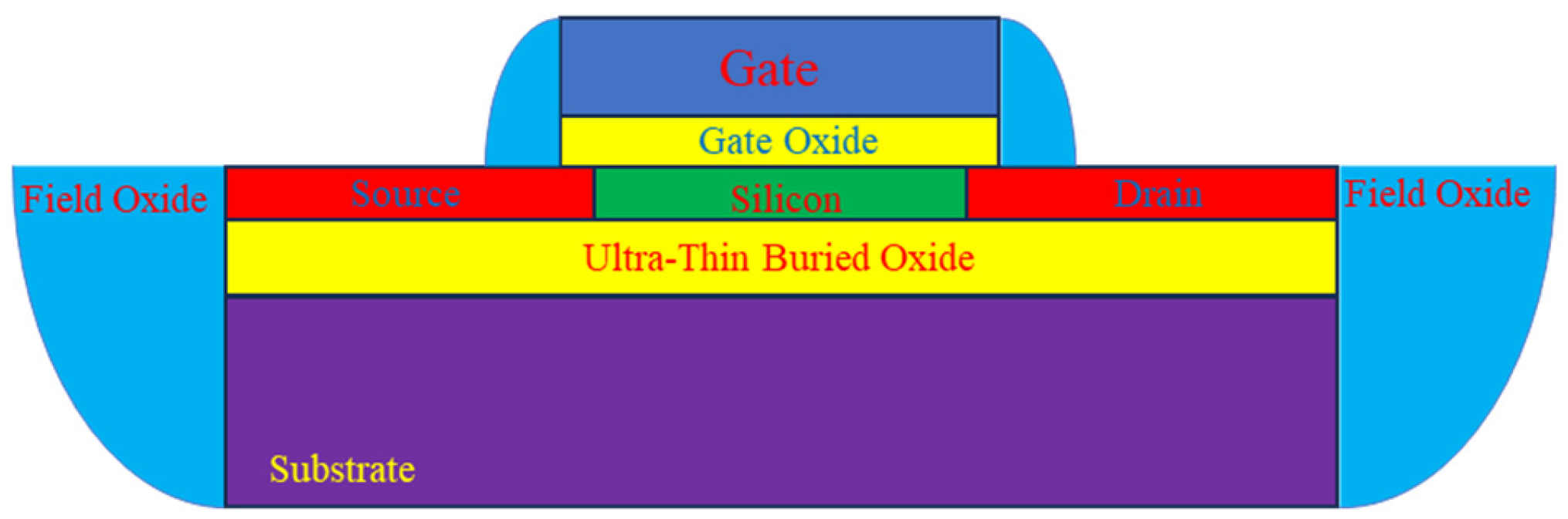
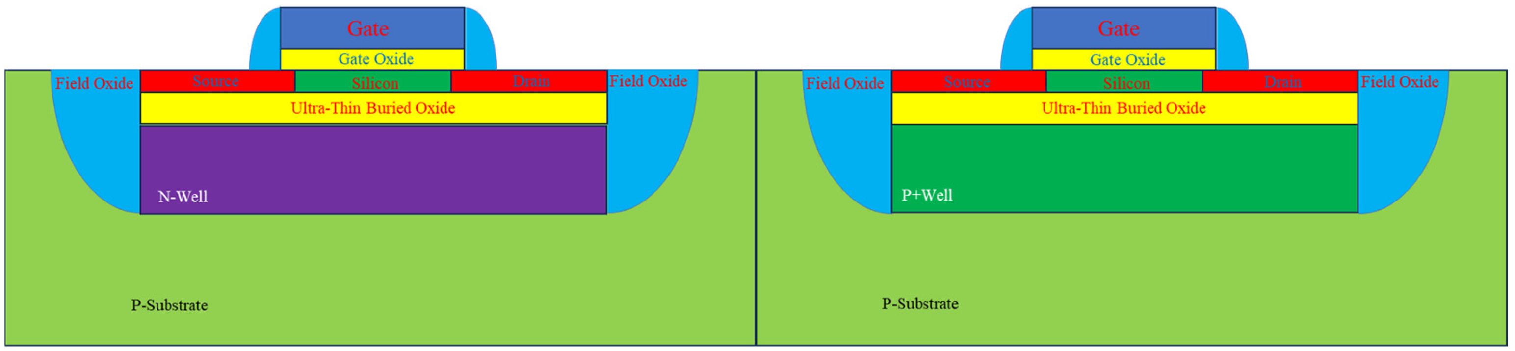
8]. SRAM designed using a 22 nm FDSOI integrated circuit process has not been studied through particle radiation experiments. Therefore, an SRAM was designed using a 22 nm FDSOI integrated circuit process to quantify the effects of particle radiation on the SRAM. Due to the high insulation properties of the buried oxygen layer, the control effect of the gate of an FDSOI transistor is enhanced, as shown in
Figure 1. In China, the 22 nm FDSOI integrated circuit process node is developing rapidly and is gradually being mass-produced at a large scale. Due to the presence of buried oxygen layers, bipolar transistors parasitized by field-effect transistors will not form latch-up effects, reducing the application of irradiation-hardened technology and improving the utilization rate of the wafer area.
In space, there are a large number of rays and particles, and the SRAM module in space-based artificial intelligence systems is inevitably exposed to radiation from rays and particles. In order to quantify the impact of particles on SRAM modules, this design adopts an advanced domestic 22 nm FDSOI CMOS integrated circuit process and designs an SRAM module [
9,
10]. In the peripheral circuit, depending on the different applications required in information systems, some use EDAC technology, while others do not [
11]. Whether it is a bulk silicon CMOS integrated circuit process or an FDSOI CMOS integrated circuit process, the core aim is to form a current through the inversion layer of the homogeneous impurity semiconductor under the action of voltage.
Simulation and verification are two methods for studying single-event effects. There are more studies on single-event upsets caused by particle radiation in bulk silicon integrated circuit processes, and fewer studies on single-event upsets caused by particle radiation in an FDSOI integrated circuit process. From the perspective of the transistor structure, the non-equilibrium charge carriers caused by particle irradiation collected by sensitive nodes, as well as parasitic bipolar effects, are the main reasons for the generation of single-event transients.
2. Device and Simulation Details
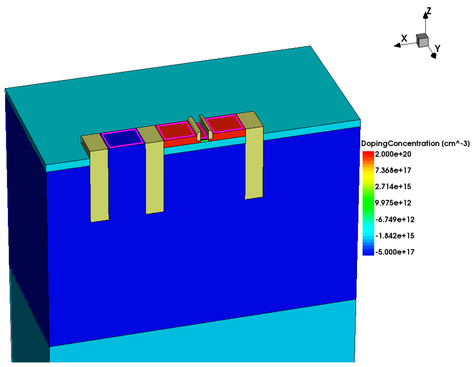
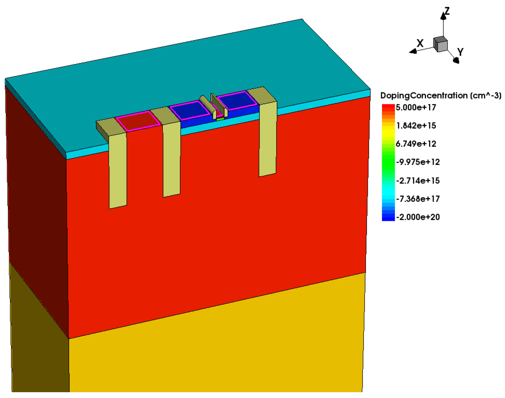
Based on the design rule kit provided by the process manufacturer, The NMOS transistor model structure and PMOS transistor model structure were constructed using the 2024 version of Technology Computer-Aided Design (TCAD) software to theoretically analyze the performance of integrated circuit process devices.
Figure 2 presents a 3D structural diagram of an NMOS transistor, and
Figure 3 shows a 3D structural diagram of a PMOS transistor. For metal oxide semiconductor field-effect transistors, the source and drain structures are completely symmetrical, and when in use, they are only connected at different potentials.
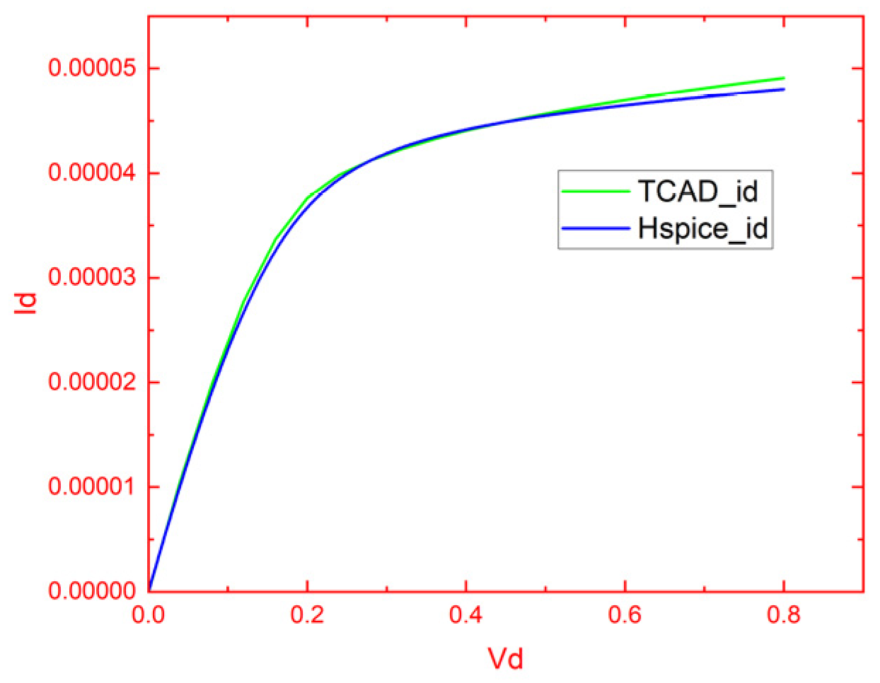
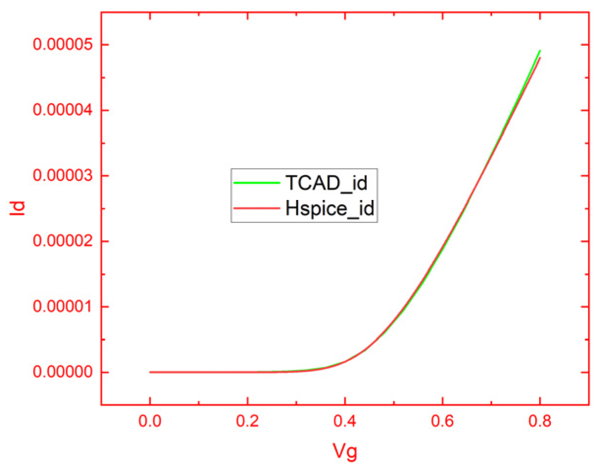
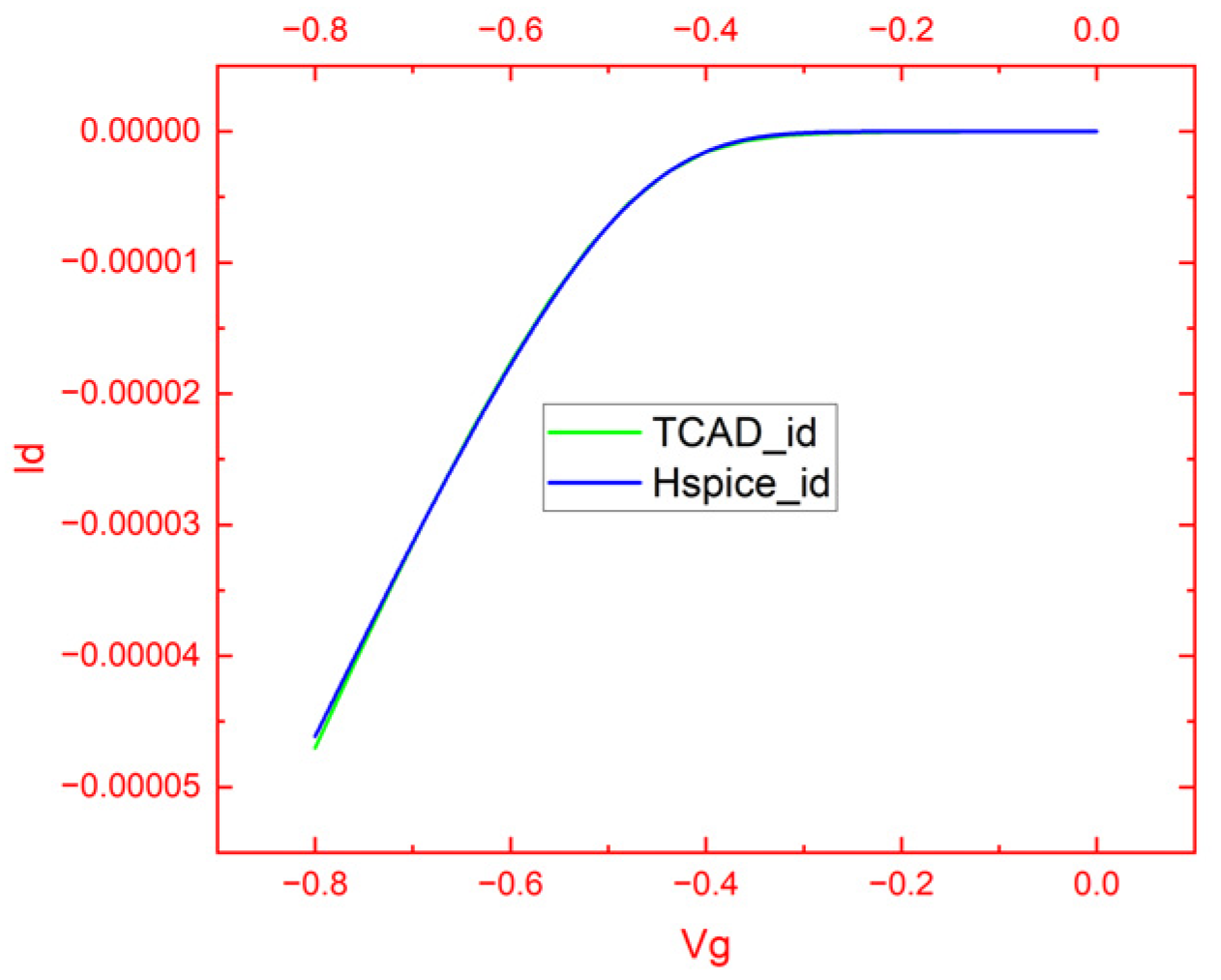
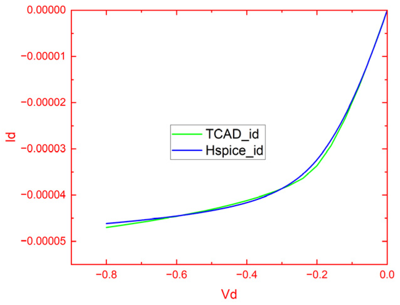
In order to make the parameters of the transistor model as close as possible to the actual transistor parameters, the transfer characteristic curve and output characteristic curve of the transistor model need to be calibrated so as to truly reflect the performance of the actual transistor. The characteristic curves of field-effect transistors were calibrated according to the integrated circuit process design kit.
Figure 4 shows the transfer characteristic curve of an NMOS transistor,
Figure 5 shows the output characteristic curve of an NMOS transistor,
Figure 6 shows the transfer characteristic curve of a PMOS transistor, and
Figure 7 shows the output characteristic curve of a PMOS transistor. The maximum scanning calibration voltage is 0.8 v.
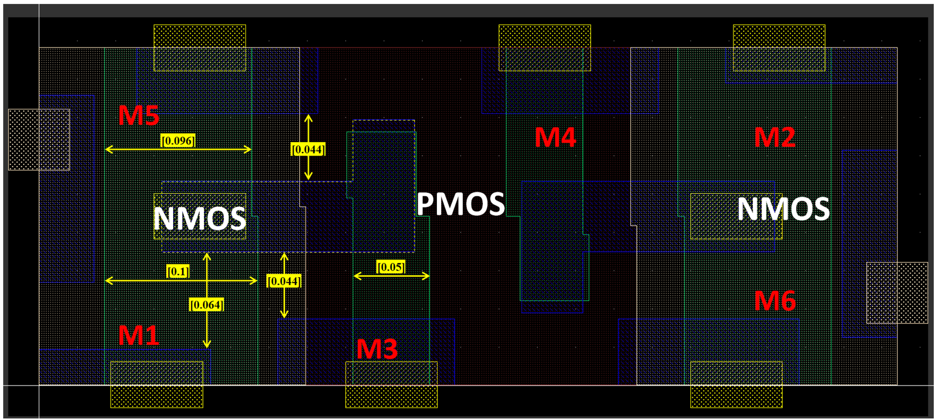
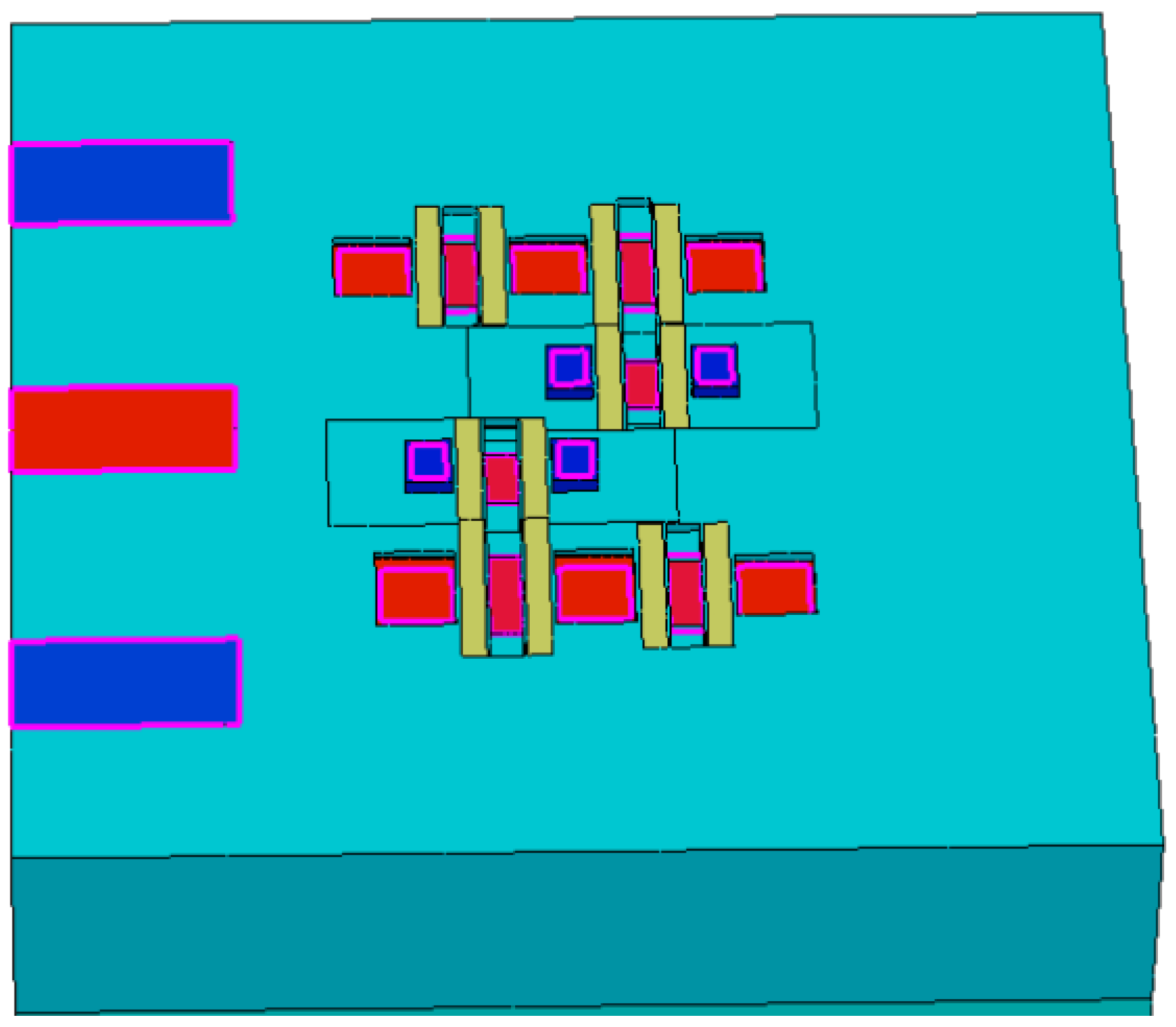
According to the structure of an FDSOI transistor, the buried oxygen layer is above the substrate, below the thin silicon layer, source, and drain. The W/L ratio of the FDSOI NMOS was 0.1/0.03 µm in the TCAD model and the W/L ratio of the FDSOI PMOS was 0.05/0.03 µm in the TCAD model. An SRAM was designed using the process design kit provided by the integrated circuit process manufacturer. Its layout structure is shown in
Figure 8 and was based on the design rules. The SRAM cell structure was constructed using Technology Computer-Aided Design (TCAD) software, and the 3D structure of the SRAM is shown in
Figure 9.
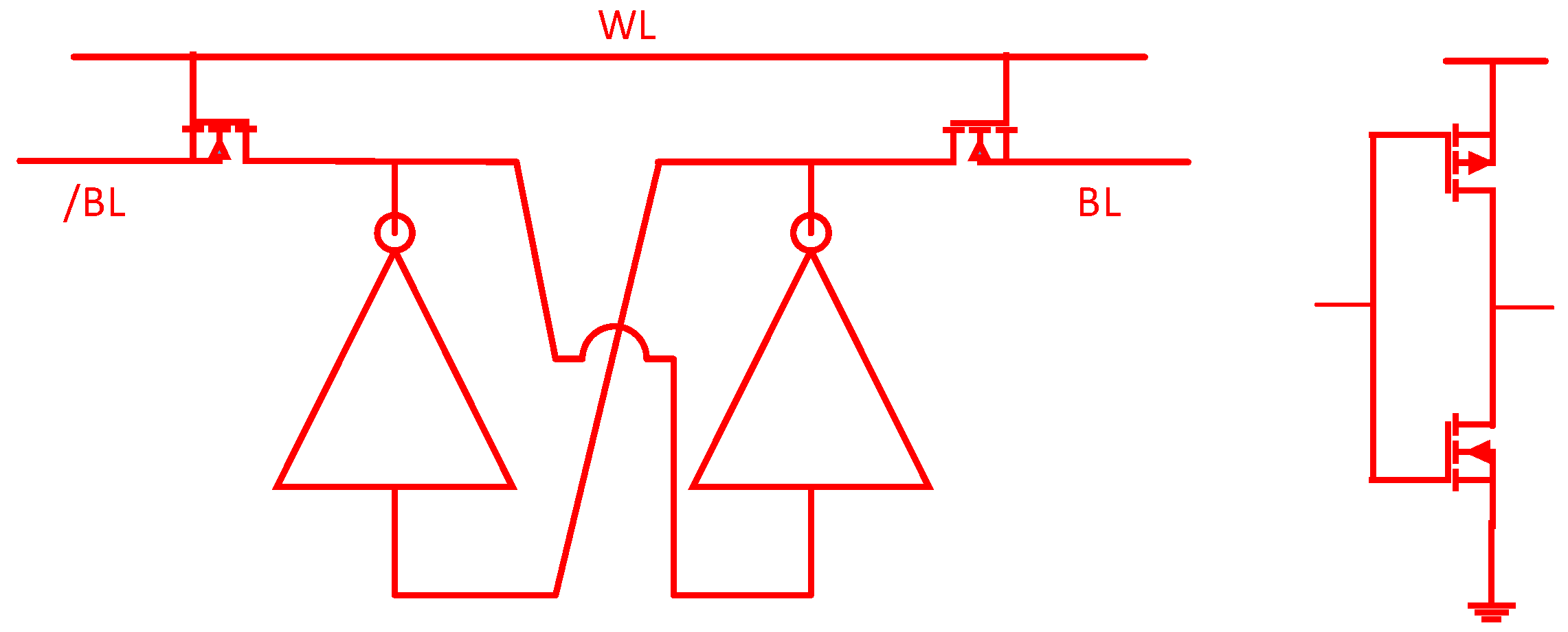
A single SRAM cell consists of two inverters forming a bi-stable structure, and two NMOS transistors forming a transmission channel. Under the action of a read signal, the storage state of the bi-stable structure is obtained. The SRAM structure is shown in
Figure 10.
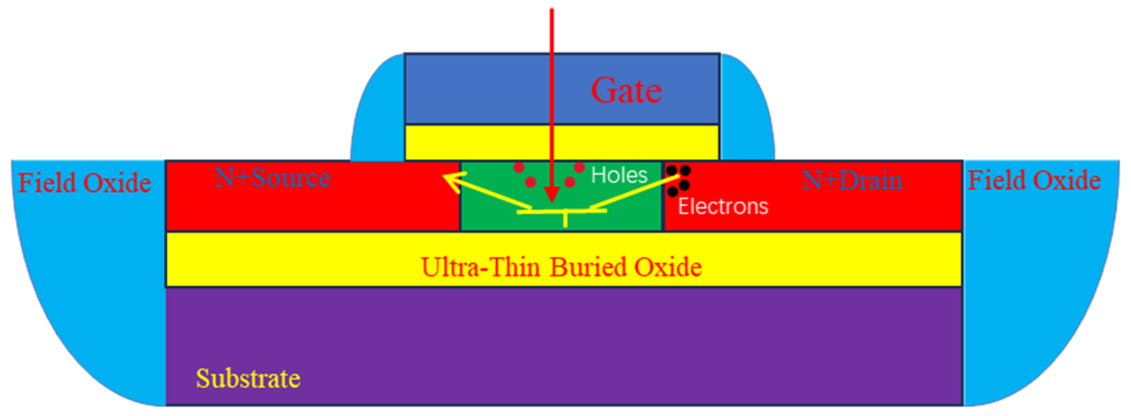
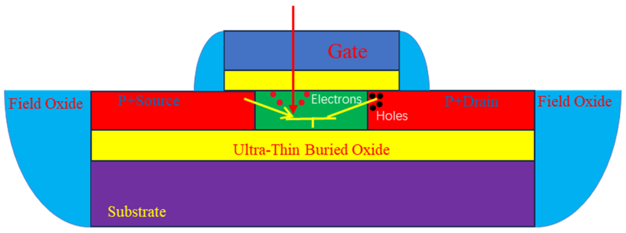
For the FDSOI integrated circuit process, the NMOS transistor forms a parasitic NPN bipolar transistor between the thin silicon, source, and drain; the PMOS transistor forms a parasitic PNP bipolar transistor between the thin silicon, source, and drain. When particles radiate on the NMOS transistor of the FDSOI integrated circuit process, a large number of non-equilibrium carriers are generated along the particle motion trajectory. Unbalanced electrons are absorbed by the drain, leaving non-equilibrium holes in the thin silicon. Due to the buried oxygen effect, these non-equilibrium holes cannot enter the underlying substrate. These holes raise the potential of the thin silicon, which can easily cause parasitic bipolar transistors to conduct and flip the state of the SRAM cell [
12]. A schematic diagram of the parasitic bipolar transistor is shown in
Figure 11. Particle radiation in PMOS transistors can also produce similar effects, as shown in
Figure 12.
3. Simulation Results
The ability of impurity semiconductors to conduct electricity is determined by the carrier concentration and the voltage applied to it. The carrier concentration is related to doping, and usually the majority carrier concentration is equal to the doping concentration. The minority carrier concentration is determined by Formula (1).
and
are the concentrations of electrons and holes in impurity semiconductors,
is the intrinsic carrier concentration at a certain temperature, and the carrier concentration is determined by Formula (2).
is the effective state density of the conduction band, and
is the effective state density of the valence band [
13,
14].
In equilibrium, the current density is determined by Formula (3), where
is the electron density,
is the hole density,
is the electron charge,
is the electron mobility,
is the hole mobility, and
is the electric field strength.
In non-equilibrium conditions, the current density is determined by Formula (4), where
is the Boltzmann constant,
is the absolute temperature,
is the concentration gradient of electrons, and
is the concentration gradient of holes.
In order to achieve a regular distribution of NMOS and PMOS transistors, the P-well of the NMOS transistor and the N-well of the PMOS transistor are alternately placed, as shown in
Figure 13. At the same time, a PN junction naturally forms between the N-well and P-well. The PN junction between the wells greatly reduces the influence of the leakage current of different types of transistors under the action of reverse bias voltage. The leakage current formula is shown in (5), where
is the electron diffusion coefficient,
is the hole diffusion coefficient,
is the diffusion length of minority carrier holes, and
is the diffusion length of minority carrier electrons.
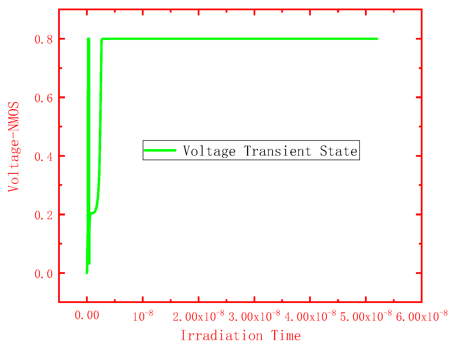
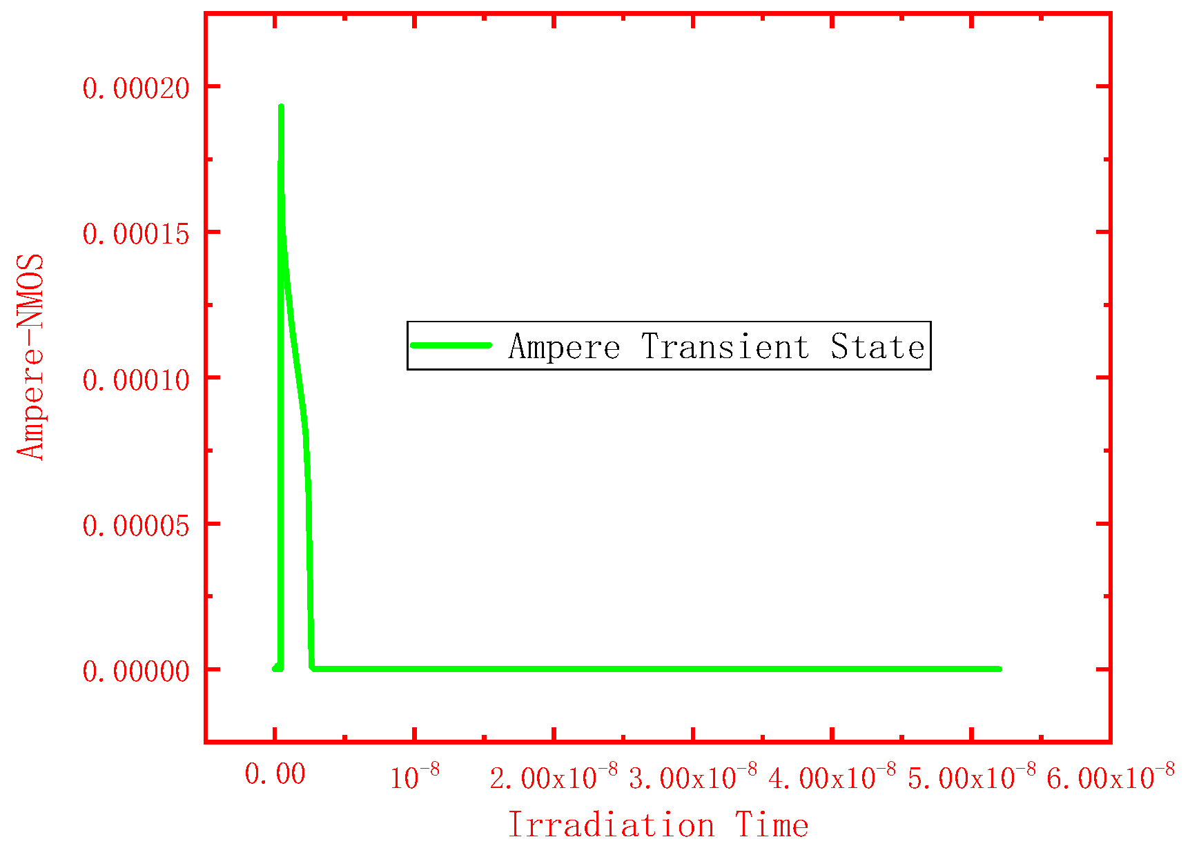
When particles radiate semiconductor materials, a large number of non-equilibrium charge carriers are generated along the particle trajectory, forming non-operational pulses at sensitive nodes and affecting the expression of logical states. When the particle energy is low, the non-equilibrium carriers generated by particle-induced radiation effects in SRAM cells are not sufficient to change the logical state of the SRAM cell. When the SRAM has high potential, the voltage and current transients of the NMOS transistor in the closed state under particle radiation are as shown in
Figure 14 and
Figure 15.
4. Experimentation Results and Discussion
A fully customized SRAM module with a capacity of 44 Kbits was designed using a domestic 22 nm FDSOI integrated circuit CMOS process, and a 1.375 Mbits SRAM array was composed of 32 × 44 Kbits SRAM modules. In the peripheral circuit, an SRAM array adopts EDAC technology, which adds a certain structure of logic circuits to the system. These logic circuits ensure the correctness of the SRAM cell data, reduce the probability of soft errors, and achieve a balance between read speed and correctness; an SRAM array does not use EDAC technology.
The experimental setup is as follows: the data format stored in the SRAM arrays is a checkerboard distribution, and the Field-Programmable Gate Array (FPGA) is responsible for communicating with the SRAM arrays. The computer controls the FPGA through control software to read data from the low address to the high address of the SRAM arrays. The FPGA reads out the data from the SRAM arrays when it is irradiated by particles and sends it to the computer for storage. Then, data from the SRAM arrays are compared with the original data in the SRAM arrays to determine which SRAM cells have flipped, and the SRAM cell information is rewritten based on the specific addresses for the next cycle of particle irradiation. SRAM arrays are placed in the irradiation area, and computers and FPGA are kept away from the irradiation area to avoid particle radiation.
When using Kr particles to radiate SRAM arrays with different peripheral circuits, the SRAM array without EDAC technology had 6486 cell upsets, 15 instances of 2-cell upsets, and no multi-cell upsets; the SRAM array using EDAC technology has no single-cell upsets, 430 two-cell upsets and one instance of multi-cell upsets. When the SRAM arrays with EDAC technology are irradiated with particles, only correct one instance of error can be corrected. When two or more errors occur, the EDAC system is unable to correct them. Therefore, under Kr particle radiation, the SRAM with an EDAC system was found to have 430 two-cell upsets and one multi-cell upset.
The total dose of Kr particles is 5 × 10 × 6 particles/cm
2, and the injection rate is 1.20 × 10 × 4 particles/cm
2s. The Kr particle energy is 449.2 MeV, the range in silicon is 54.9 μm, and the linear energy transfer (LET) is 37.9 MeV.
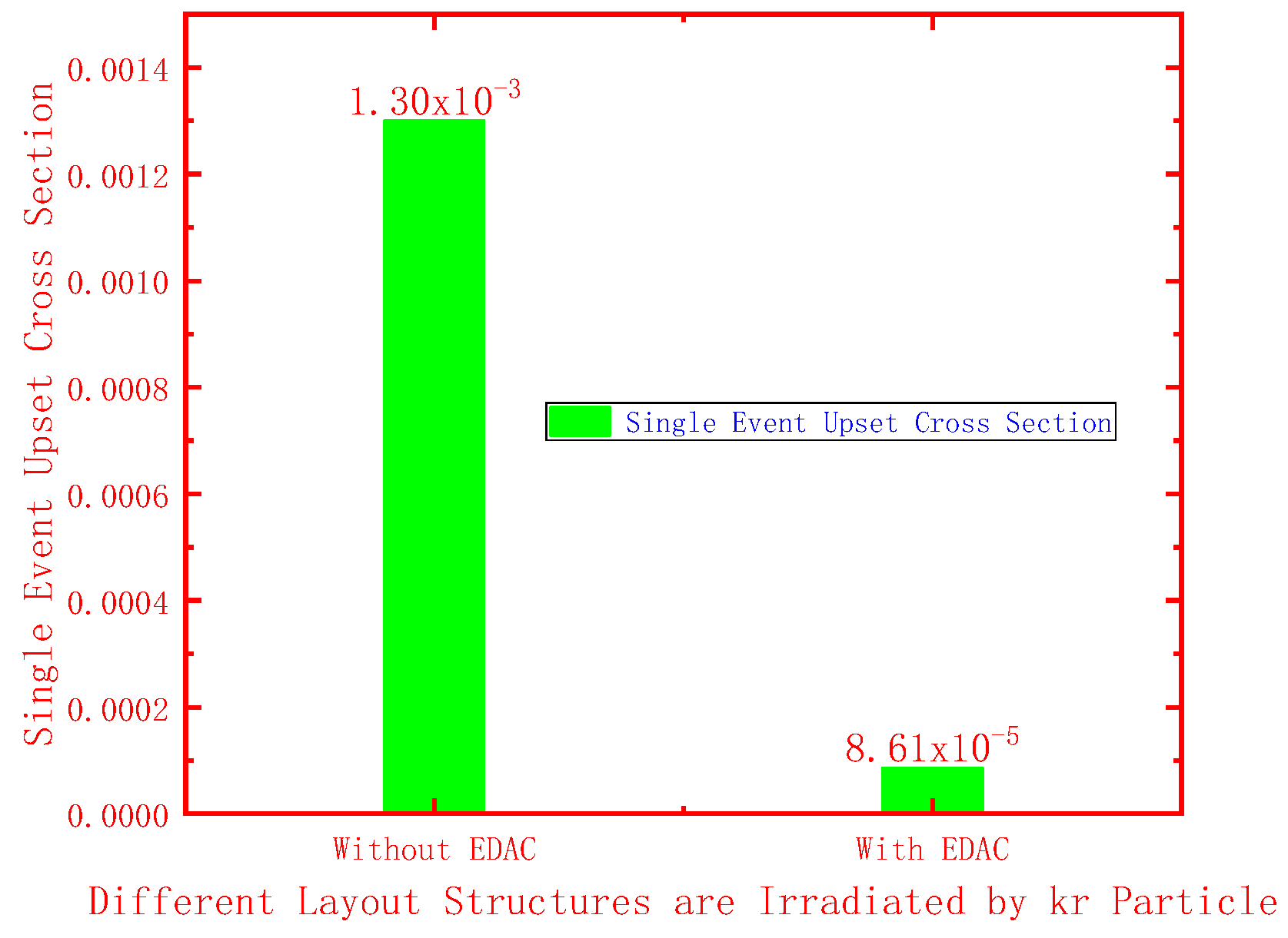
Figure 16 shows the different cross-sectional areas of single-event upsets under Kr particle radiation for layout structures with and without EDAC [
15].
Figure 16 shows the cross-sectional areas of cell upsets in SRAM module arrays with and without EDAC technology under Kr particle radiation. This irradiation of SRAM arrays was conducted in the space comprehensive irradiation environment simulation system of the Harbin Institute of Technology.
5. Conclusions
This paper describes the design of a fully customized 44 Kbits SRAM using domestic 22 nm FDSOI CMOS integrated circuit technology, using a 1.375 Mbits SRAM array to verify the SRAM cell-upset characteristics caused by Kr particle radiation. Under Kr particle irradiation, the SRAM array without EDAC technology had 6486 cell upsets, 15 instances of 2-cell upsets, and no multi-cell upsets. In the SRAM array using EDAC technology, under Kr particle radiation, there was no single-cell upset, 430 two-cell upsets, and one multi-cell upset. Reducing the number of soft errors can generally be achieved by combining irradiation-hardened technology with EDAC technology. From the number of cell upsets of SRAM module arrays observed when using EDAC technology, it can be seen that EDAC technology plays a significant role in the irradiation-hardened technology of SRAM. This provides strong support for fully utilizing EDAC technology to enhance irradiation-hardened digital integrated circuits. Mastering the physical mechanism of SRAM cell upsets and using irradiation-hardened technology to achieve certain design goals are the main ways to design aerospace integrated circuit information systems.
Author Contributions
Conceptualization, X.Y. and J.Z.; methodology, J.C.; software, X.J.; validation, Y.C., X.Y. and Y.C.; formal analysis, X.Y.; investigation, X.J.; resources, J.C.; writing—original draft preparation, J.Z.; writing—review and editing, X.Y.; visualization, T.C.; supervision, J.C.; project administration, J.C.; funding acquisition, J.Z. All authors have read and agreed to the published version of the manuscript.
Funding
This research was funded by Guangxi Natural Science Foundation Joint Special Project (Guilin University of Aerospace Technology), grant number 2026GXNSFHA00640048.
Data Availability Statement
The original contributions presented in this study are included in the article. Further inquiries can be directed to the corresponding author.
Conflicts of Interest
The authors declare no conflicts of interest.
References
- Cai, C.; Hu, M.; Shen, L.; Yu, J.; Chen, G. Design and Evaluation of a Radiation-Hardened FDSOI SRAM with High-Reliable Elements and Power Management Circuits for Space Application. IEEE Trans. Aerosp. Electron. Syst. 2025, 61, 5057–5066. [Google Scholar] [CrossRef] [Scilit]
- Cai, C.; Liu, Y.; Hu, M.; Chen, G.; Yu, J. Characterization of LDO Induced Increment of SEE Sensitivity for 22 nm FDSOI SRAM. IEEE Trans. Device Mater. Reliab. 2023, 23, 537–543. [Google Scholar] [CrossRef] [Scilit]
- Cai, C.; Zhao, P.X.; Xu, L.W.; Liu, T.Q.; Li, D.Q.; Ke, L.Y.; He, Z.; Liu, J. SEU tolerance improvement in 22 nm UTBB FDSOI SRAM based on a simple 8T hardened cell. Microelectron. Reliab. 2019, 100–101, 113322. [Google Scholar] [CrossRef] [Scilit]
- Haran, A.; Keren, E.; David, D.; Refaeli, N.; Giterman, R.; Assaf, M.; Atias, L.; Teman, A.; Fish, A. Single-Event Upset Tolerance Study of a Low-Voltage 13T Radiation-Hardened SRAM Bitcell. IEEE Trans. Nucl. Sci. 2020, 67, 1803–1812. [Google Scholar] [CrossRef] [Scilit]
- Luo, Y.-Y.; Chen, W.; Zhang, F.-Q.; Wang, T. Influences of supply voltage on single event upsets and multiple-cell upsets in nanometer SRAM across a wide linear energy transfer range. Chin. Phys. B 2021, 30, 679–688. [Google Scholar] [CrossRef] [Scilit]
- Huang, Z.-Q.; Jing, H.-T.; Mo, L.-H.; Hu, Z.-L.; Shen, G.-P.; Zhou, Z.-H.; Cai, C. Research of hardening strategies based on the single event effect induced by atmospheric-like neutrons. Nucl. Eng. Technol. 2025, 57, 103666. [Google Scholar] [CrossRef] [Scilit]
- He, Z.; Zhao, S.-W.; Liu, T.-Q.; Cai, C.; Yan, X.-Y.; Gao, S.; Liu, Y.-Z.; Liu, J. Verification of SEU resistance in 65 nm high-performance SRAM with dual DICE interleaving and EDAC mitigation strategies. Nucl. Sci. Tech. 2021, 32, 139. [Google Scholar] [CrossRef] [Scilit]
- Wang, J.; Wu, X.; Tian, H.; Li, L.; Shi, S.; Chen, L. Radiation Tolerant SRAM Cell Design in 65nm Technology. J. Electron. Test. 2021, 37, 255–262. [Google Scholar] [CrossRef] [Scilit]
- Xu, J.-Y.; Chen, S.-M.; Song, R.-Q.; Wu, Z.-Y.; Chen, J.-J. Analysis of single-event transient sensitivity in fully depleted silicon-on-insulator MOSFETs. Nucl. Sci. Technol. 2018, 29, 108–113. [Google Scholar] [CrossRef] [Scilit]
- Yin, Y.; Ma, H.; Zheng, Q.; Chen, J.; Duan, X.; Zhang, P.; Zhou, X. Total ionizing dose and single event effect response of 22 nm ultra-thin body and buried oxide fully depleted silicon-on-insulator technology. Microelectron. Reliab. 2024, 152, 115296. [Google Scholar] [CrossRef] [Scilit]
- Jo, E.; Yoon, H.; Park, H.; Choi, W.-y.; Kwon, I. Radiation tolerant capacitor-SRAM without area overhead. Nucl. Eng. Technol. 2024, 56, 2916–2922. [Google Scholar] [CrossRef] [Scilit]
- Lv, Y.; Xie, T.; Liu, Y.; Ren, Z.; Chen, J. Area-efficient radiation-hardened 6 T SOI SRAM cell design using TDBC Transistors. Microelectron. Reliab. 2023, 142, 114911. [Google Scholar] [CrossRef] [Scilit]
- Wu, X.; Mori, T.; Liu, W. Thermoelectric stability as a design constraint for energy conversion. Joule 2026, 10, 102421. [Google Scholar] [CrossRef] [Scilit]
- Wu, X.; Ye, C.; Wang, Y.; Liao, Z.; Zhang, W.; Liu, W. Negative enthalpy delivering improved thermal stability for Mg2Sn-based thermoelectric power generator. Acta Mater. 2025, 289, 120865. [Google Scholar] [CrossRef] [Scilit]
- Zhao, P.; Li, B.; Liu, H.; Yang, J.; Jiao, Y.; Chen, Q.; Sun, Y.; Liu, J. The Effects of Total Ionizing Dose on the SEU Cross-Section of SOI SRAMs. Electronics 2022, 11, 3188. [Google Scholar] [CrossRef] [Scilit]
| Disclaimer/Publisher’s Note: The statements, opinions and data contained in all publications are solely those of the individual author(s) and contributor(s) and not of MDPI and/or the editor(s). MDPI and/or the editor(s) disclaim responsibility for any injury to people or property resulting from any ideas, methods, instructions or products referred to in the content. |





 ,
,