Article

A Multi-Port Wireless Energy Interaction System Based on LC Series Resonance with Seamless Mode Switching Capability


1
School of Automation, Jiangsu University of Science and Technology, Zhenjiang 212000, China
2
Division of Electronics and Informatics, Gunma University, Kiryu 376-8515, Japan
3
School of Intelligent Manufacturing, Yangzhou Polytechnic Institute, Yangzhou 215126, China
*
Author to whom correspondence should be addressed.
Symmetry 2026, 18(3), 447; https://doi.org/10.3390/sym18030447
Submission received: 30 January 2026 / Revised: 20 February 2026 / Accepted: 3 March 2026 / Published: 5 March 2026

Abstract

To address the challenges associated with inter-module energy interaction and mode adjustment at load ports in distributed energy systems in the context of the energy transition, this paper proposes and designs a multi-port wireless energy interaction system based on LC series resonance and multi-coil magnetic coupling. The system aims to facilitate flexible energy interaction among power sources, energy storage units, and loads, as well as multi-modal port regulation. The system employs a multi-coil coupled full-bridge topology combined with a phase-shift control strategy to achieve energy exchange and power regulation among multiple ports. To meet the power demands of different ports, a port state control method incorporating a mode preset mechanism is proposed, enabling the intermediate port to switch seamlessly among input (source), output (load), and active relay modes. This paper analyzes the operating modes of a single port and establishes the dynamic mathematical model of the overall three-coil system as well as the small-signal model of the port output. Furthermore, it investigates the energy interaction mechanism to derive the operating characteristics and conditions under different modes, and elucidates the energy relay mechanism with zero active power consumption. A three-port hardware experimental platform was constructed based on a dsPIC33 controller. Experimental results indicate that: (1) the prototype achieved a maximum transmission power of 100 W; (2) the peak system efficiency reached 83.1 % under different load conditions; and (3) during mode switching, the system response time was less than 200 ms with no significant overshoot. The study demonstrates that the proposed topology and control strategy effectively realized dynamic energy interaction and seamless mode switching among multiple ports, providing a theoretical basis and engineering reference for multi-port energy interaction and wireless power transfer networks.

1. Introduction

In recent years, with the transition of traditional energy sources, research and application of Wireless Power Transfer (WPT) technology have gradually increased in green energy due to its flexibility and safety. Wireless power transfer technology achieves energy transmission through magnetic coupling. As it enables energy transfer through air, it offers non-contact operation and high flexibility. This technology provides electrical isolation between input and output, effectively preventing wear and aging caused by manual connection or disconnection in wired systems, thus reducing the risk of failure.
Currently, this technology has been applied in fields such as rail transit [1,2], new energy vehicles [3], microgrid systems [4], and consumer electronics [5]. In this paper, WPT technology is applied to multi-port systems to achieve wireless energy interconnection and flexible interaction among sources, storage, and loads. The proposed multi-port system can be utilized for the organic integration of power supply, energy storage, and loads in distributed generation units to realize energy interconnection.
In research on the architecture of multi-port WPT systems, traditional systems predominantly adopt the ’single-transmitter to multi-receiver’ architecture [6,7,8,9]. Refs. [6,7] employ multiple receiver coils at the receiving side and multiple transmitter coils at the transmitting side, respectively, to enhance the system’s transmission power and load-carrying capacity. Meanwhile, Refs. [8,9] increase the number of supported loads by adding transmitter coils and their corresponding receiver coils. However, such architectures mainly rely on fixed ’multi-transmitter’ or ’multi-receiver’ modes. This reliance not only imposes strict limitations on transmission distance but also results in fixed port functions, thereby failing to satisfy the requirements for bidirectional energy flow between nodes and port mode switching.
To overcome the limitations on transmission distance, the introduction of relay coils has emerged as a mainstream solution [10]. Refs. [11,12] investigated topological structures achieving constant output current (CC) and constant output voltage (CV) for multi-port and multi-load applications involving multiple relay coils, respectively. Ref. [13] utilized a dual-frequency inverter and relay coil transmission to enhance both transmission distance and load-carrying capacity by configuring different load frequencies, while Ref. [14] employed relay coils to alter the direction of energy flow while simultaneously extending the transmission distance. Furthermore, structural design optimization of relay coils can achieve decoupling between coils [15], thereby enhancing coordination between the transmitting and receiving coils. Ref. [16] adopted a bipolar coil structure to supply power to three loads, simultaneously achieving coil decoupling and constant voltage output. Ref. [17] proposed a vertically overlapped double-layer coil structure to integrate the coils within a single plane, which realized decoupling and improved the interoperability between coils of different shapes. Ref. [18] utilized decoupled Double-D (DD) and rectangular coil structures to facilitate bidirectional energy interaction. However, the relay ports in the aforementioned studies typically function solely as passive energy ’channels’ and cannot directly participate in energy management as active power sources or loads. This characteristic limits the flexibility of the system within multi-port networks and represents a significant challenge that urgently needs to be addressed in current multi-port WPT systems.
In terms of control strategies, achieving precise power flow control among multiple ports is critical. Phase-Shift Control (PSC) based on full-bridge or half-bridge topologies is a commonly used method. Refs. [19,20] proposed a dual-side asymmetric voltage cancellation control method and a method for regulating the primary and secondary phase difference based on PSC, respectively, thereby realizing bidirectional energy flow. Refs. [21,22] proposed zero-power-flow control and current balancing strategies based on Hybrid Phase-Shifted Control (HPSC), which achieved energy management for idle ports and balanced current distribution. Ref. [23] adopted Pulse Frequency Modulation (PFM) technology to enable specific loads to receive wireless power via frequency selection. Ref. [24] combined HPSC with a modular stacked decoupling design of coils to achieve transmission direction control and power regulation. Ref. [25] employed a combination of PWM and PSC to realize energy transmission and power flow control among three ports. Despite the fact that the aforementioned control methods have effectively addressed issues such as bidirectional power transfer and multi-port load allocation, few studies have proposed solutions for the dynamic mode switching of port functions.
To address the challenges regarding inter-module energy interaction and mode switching during port function multiplexing in multi-port WPT systems, this paper proposes a multi-port wireless energy interaction system based on LC series resonance and multi-coil coupling. By introducing a port mode preset mechanism, the complexity of system control is reduced. Simultaneously, phase control enables the implementation of three modes for intermediate ports—input, output, and relay (neither input nor output)—along with their corresponding power control. Furthermore, this paper provides an in-depth analysis of the power transfer mechanisms under different port states. Investigates the operating modes of the LC series resonant network when it functions as an energy transmitter, receiver, or active relay, which realizes the energy-interaction between multiple ports and the switching of port modes, and improves the distance of wireless energy transmission.
The remainder of this paper is organized as follows. Section 2 presents the structure and topology of the proposed system in detail. Section 3 develops and analyzes the corresponding mathematical model. Section 4 illustrates the port control strategy and small-signal modeling of ports for wireless multiport systems. The simulation and experimental results are provided in Section 5, and conclusions are drawn in Section 6.

2. Structure and Topology of Multi-Port Wireless Energy Transfe  Systems

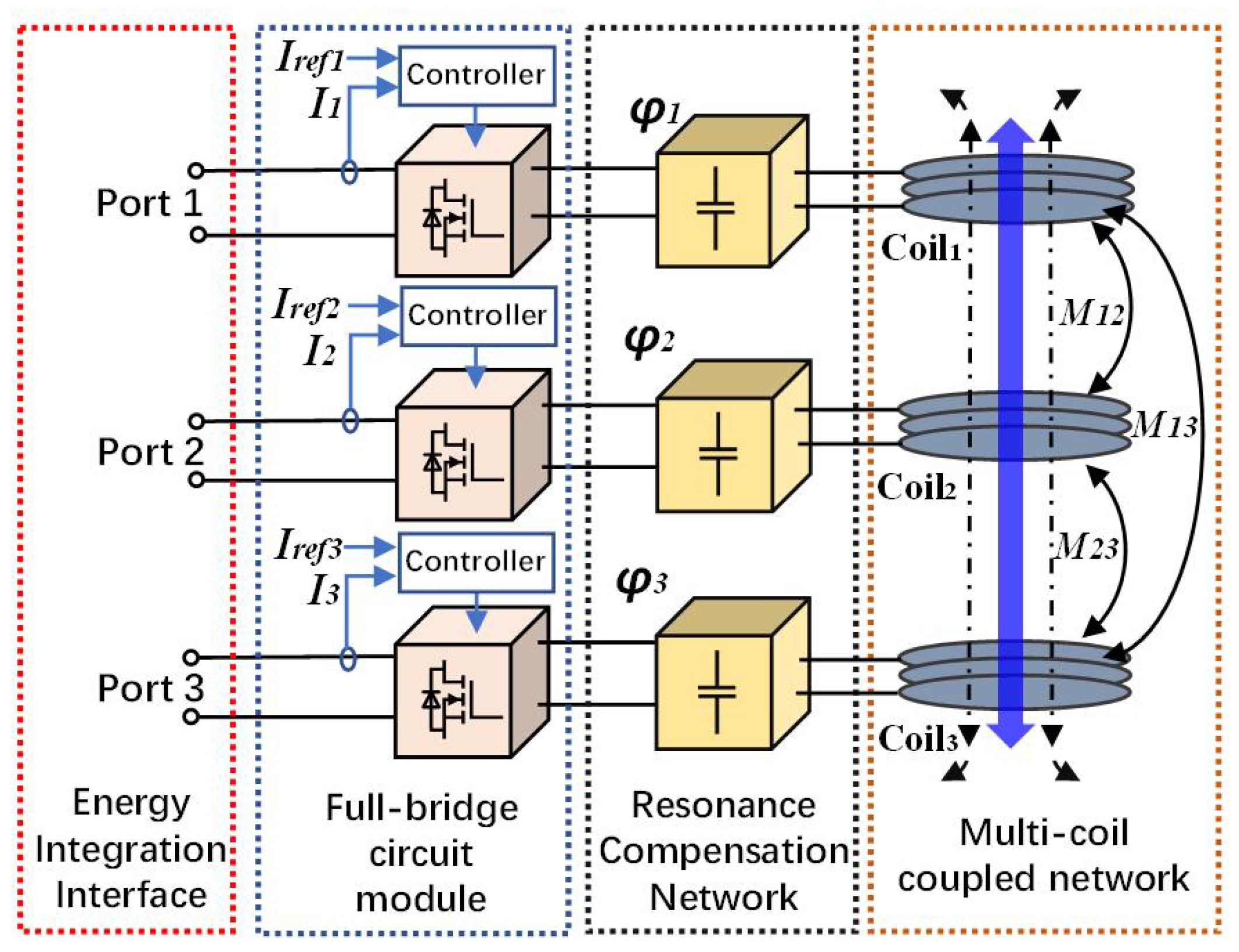
The structure of the multi-coil coupled wireless power exchange system proposed in this paper is shown in Figure 1. The system consists of three structurally symmetric energy transceiver modules, each employing a circuit architecture that cascades a full-bridge converter with an LC series resonant network. Wireless power exchange between modules is achieved through high-frequency magnetic field coupling via coil arrays, with the full-bridge converter performing power conversion between high-frequency AC and port DC.
Utilizing the full-bridge topology and the ‘Energy Integration Interface’ design, the system modules exhibit high port compatibility. They can function either as source terminals interfacing with DC power supplies or energy storage units of various voltage and power levels, or as load terminals connected to resistive loads. Regarding the control strategy, phase-shift control is adopted. By regulating the phase angles ( φ 1 , φ 2 , φ 3 ) of the full-bridge output voltages, the energy excitation of the LC resonant network is modulated, thereby controlling the input/output power of the ports. Consequently, this regulation mechanism enables seamless switching among three operating modes—input, output, and Active Relay (where the coil operates in relay mode with zero port power)—as well as precise control over the direction and magnitude of the power flow between modules.
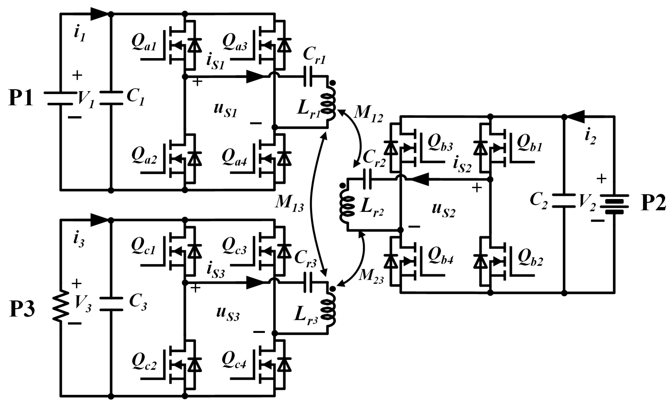
The circuit topology of the proposed system is depicted in Figure 2. Here, V 1 V 3 denote the terminal voltages on the DC-side of the ports, and C 1 C 3 represent the DC-link capacitors. L r i and C r i ( i = 1 , 2 , 3 ) correspond to the resonant inductance and resonant capacitance of port P i , respectively, which together constitute the LC series resonant network for the i-th port. Furthermore, u S 1 u S 3 and i S 1 i S 3 represent the output voltages of the full-bridge and the resonant tank currents, respectively. Finally, i 1 i 3 denote the DC-side currents of ports P 1 P 3 .

3. Mathematical Modeling and Modal Analysis of Energy Interaction Systems

To maximize power-transfer capacity and operating efficiency, symmetric parameterization is adopted for all ports. As a result, the three series-resonant tanks are designed to have identical resonant frequencies, i.e., f s = f r 1 = f r 2 = f r 3 . Consequently, the resonant inductors and capacitors are chosen to be identical: L r 1 = L r 2 = L r 3 and C r 1 = C r 2 = C r 3 . In the modeling process, the parasitic capacitance and winding resistances of the switching-device are neglected. Moreover, due to structural symmetry, the mutual inductance M i j (where i and j denote coil indices) between adjacent coils is assumed to be approximately equal, i.e., M 12 = M 23 .
Based on these assumptions, the unified resonant frequency of the system can be expressed as
f s = ω s 2 π = 1 2 π L r i C r i i = 1 , 2 , 3
As stated previously, the resonant frequency f s is identical across all resonant modules, with the corresponding angular frequency defined as ω s . The DC-link voltage of each port is indicated as V i . By employing the Fundamental Harmonic Approximation (FHA, the calculation of errors caused by harmonics is in Appendix A.) at the resonant frequency—neglecting higher-order harmonics and considering only the fundamental components—and letting φ i be the phase angle of the full-bridge output voltage at port P i , the fundamental voltage phasors U S 1 U S 3 corresponding to the instantaneous outputs u S 1 u S 3 are expressed as:
U S 1 = 4 / π V 1 φ 1 U S 2 = 4 / π V 2 φ 2 U S 3 = 4 / π V 3 φ 3
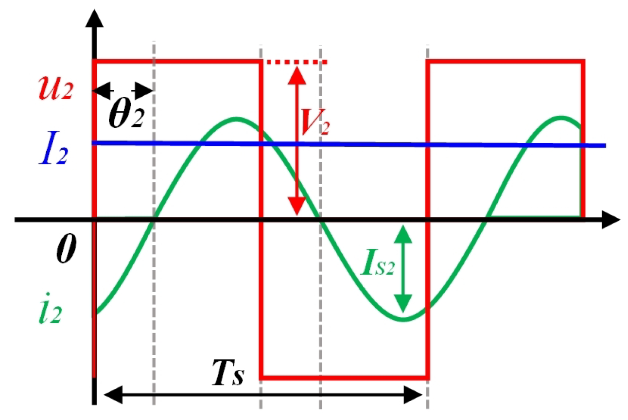
To facilitate the quantitative analysis of the three operating modes, the average values of the output currents i 1 i 3 at the ports are defined as I 1 I 3 , with a positive direction flowing from the DC source into the resonant network. Additionally, let I S 1 I S 3 denote the fundamental current phasors corresponding to i S 1 i S 3 , where I S 1 I S 3 represent their peak values. Taking port P 2 as an example, the equivalent port impedance Z e q is derived under different loading conditions. The waveforms of the resonant module current i S 2 , full-bridge voltage u S 2 , and port current i 2 are illustrated in Figure 3. Consequently, the equivalent impedance Z e q 2 of port P 2 satisfies the following conditions:
Z eq 2 = U S 2 / I S 2 = R e q 2 + j X e q 2
Within one voltage cycle T S , the magnitude of current I 2 is related to the phase difference θ i between voltage u 2 and current i 2 . Therefore, the average output current I 2 is given by the following:
I 2 = ω s 2 π 0 T S i 2 t · s g n sin ω s t d t
Based on the relationship between input voltage and current magnitude and phase at port P 2 , the following can be derived:
I 2 = ω s 2 π 0 T S I S 2 sin ω s t + θ i · s g n sin ω s t d t
where s g n ( sin ( ω t ) ) :
s g n sin ω t = 1 , ω s t 0 , π 1 , ω s t π , 2 π
Substituting Equation (6) into Equation (5) produces the relationship between the output current of port P 2 and the phase of the input module current. Its DC output current I 2 is:
I 2 = 2 I S 2 π cos θ 2
The phase difference θ 2 between the output voltage and the resonant current of the complete bridge circuit determines the average output current I 2 . This, in turn, dictates the amount of energy injected into the LC resonant network by the module and the operating mode of its ports.
From Equation (7), the direction and magnitude of the average output current I 2 at the port can characterize the input–output mode of the module. After passing through the full-bridge and LC resonant network, the equivalent DC resistance R d c 2 of the connected power supply and load is:
R d c 2 = V 2 I 2 = π V 2 2 I 2 cos θ 2
When the port is connected to a resistive load R 2 , the equivalent DC resistance R d c 2 across the full-bridge is:
R d c 2 = π R 2 2 cos θ 2
Based on the characteristics of the full-bridge circuit, the DC load resistance is transformed into an equivalent AC impedance. The equivalent AC resistance R e q 2 and reactance X e q 2 are expressed as:
R e q 2 = 4 π · V 2 I 2 cos θ 2 = 8 π 2 V 2 I 2 cos 2 θ 2 X e q 2 = R e q 2 tan θ 2 = 8 π 2 V 2 I 2 sin θ 2 cos θ 2
According to Equation (10), the equivalent impedance Z e q 2 of port P 2 in this state is:
Z e q 2 = 8 π 2 V 2 I 2 cos 2 θ 2 + j sin θ 2 cos θ 2
According to Equation (11), the full-bridge converter at each port and its subsequent circuitry can be equivalently modeled as the complex impedance Z e q i ( i = 1 , 2 , 3 ) of a resonant network terminal. Based on the characteristics of the power flow, the equivalent resistance R e q i determines the direction of the energy flow. Specifically, when Re [ Z e q i ] > 0 , the port exhibits load characteristics and absorbs power from the coupling network; when Re [ Z e q i ] < 0 , the port exhibits source characteristics and injects power into the network. In the special case where the transmitted power is zero (i.e., the DC current I i = 0 ), the port participates in magnetic coupling without consuming active power.
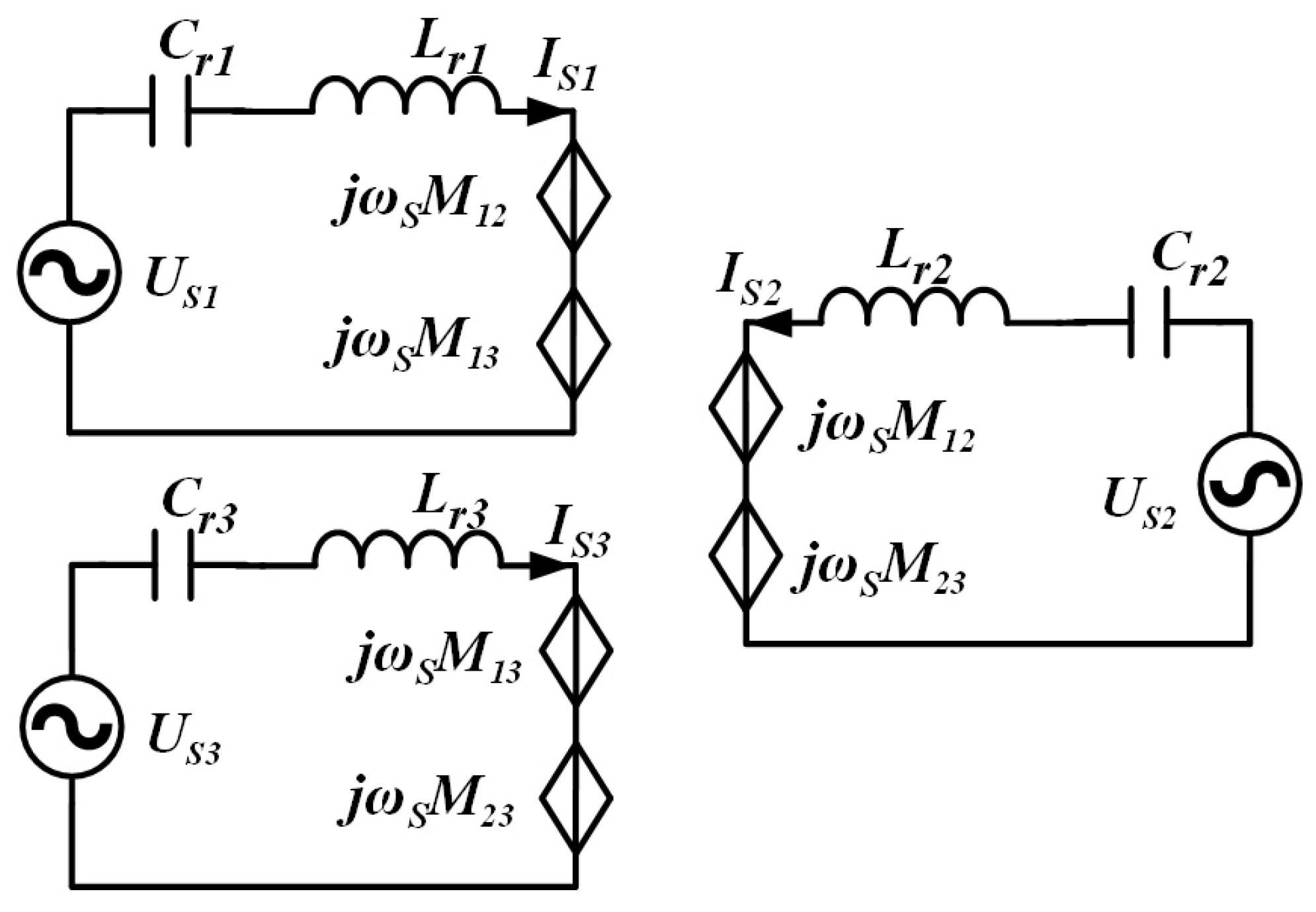
The equivalent circuit model of the system ports and the coupling network is shown in Figure 4. U S 1 U S 3 denote the equivalent excitation voltage phasors of the three ports at the resonant frequency, respectively, while the term j ω M i j I S j represents the induced voltage resulting from mutual inductance between the coils.
Based on Kirchhoff’s Voltage Law (KVL) and the magnetic-coupling relationships, the steady-state circuit equations of the system can be described as follows:
U S 1 = j ω S I S 2 M 12 + I S 3 M 13 + I S 1 X S 1 U S 2 = j ω S I S 1 M 12 + I S 3 M 23 + I S 2 X S 2 U S 3 = j ω S I S 1 M 13 + I S 2 M 23 + I S 3 X S 3
where X s i denotes the characteristic impedance of each coil circuit. In the resonant state, this represents the sum of the capacitive and inductive reactances and can be expressed as:
X S 1 = X L 1 X C 1 X S 2 = X L 2 X C 2 X S 3 = X L 3 X C 3
where the inductive reactance X l i and the capacitive reactance X c i are respectively:
X L i = ω s L r i X C i = 1 / ω s C r i
Taking the equivalent voltage phasor U S 1 of port P 1 as the reference, the voltage amplitude ratio k 1 j and the phase difference ϕ 1 j between port j and port P 1 ( j = 1 , 2 , 3 ) are defined. Consequently, the voltage relationships for the ports can be expressed as follows:
U S 2 = k 12 V 1 φ 12 U S 3 = k 13 V 1 φ 13
From the impedance analysis, the system voltage phasor matrix U is constructed and can be explicitly written as:
U = U S 1 U S 2 U S 3 = 4 / π V 1 k 11 φ 11 4 / π V 1 k 12 φ 12 4 / π V 1 k 13 φ 13
By combining Equations (12) and (16) with the matrix form of KVL, the relationship between the voltage/current phasors and the system impedance matrix is derived as:
U S 1 U S 2 U S 3 = X S 1 j ω M 12 j ω M 13 j ω M 12 X S 2 j ω M 23 j ω M 13 j ω M 23 X S 3 · I S 1 I S 2 I S 3
Since the resonant frequencies of all ports are identical, the inductive and capacitive reactances in the LC resonant networks cancel out, resulting in X S 1 = X S 2 = X S 3 = 0 . Under ideal conditions where coil internal resistances are neglected, the impedance matrix Z can be simplified as follows:
Z = 0 j ω M 12 j ω M 13 j ω M 12 0 j ω M 23 j ω M 13 j ω M 23 0
By inverting the impedance matrix Z , the admittance matrix Y of the system is obtained. Its analytical form is given by:
Y = j 2 ω M 23 M 12 M 13 1 M 12 1 M 13 1 M 12 M 13 M 12 M 23 1 M 23 1 M 13 1 M 23 M 12 M 13 M 23
Here, the admittance matrix Y is symmetric and its elements depend solely on the system’s physical structure and resonant parameters; thus, Y remains constant once the hardware configuration is determined. Based on the matrix relationship I = Y U , the current phasor I S i of the i-th port can be expressed as a linear superposition of the excitation voltages of all ports (where Y i j denotes the elements of Y ):
I S i θ i = 4 V 1 π j = 1 3 k 1 j Y i j φ 1 j
For subsequent derivations, the Euler formula is used to decompose the current phasor into its real and imaginary components. The real part Re ( I S i ) and the imaginary part Im ( I S i ) of the port current can then be expressed as:
I S i = Re I S i + j Im I S i
Re I S i = 4 π V 1 i = 1 3 k i 1 Y i 1 cos φ 1 i Im I S i = 4 π V 1 i = 1 3 k i 1 Y i 1 sin φ 1 i
By combining Equations (8) and (20), the magnitude of the current | I S i | and the phase angle θ i can be further determined:
I S i = 4 π V i i = 1 3 k i 1 Y i 1 cos φ 1 i 2 + i = 1 3 k i 1 Y i 1 sin φ 1 i 2
θ i = arc tan Im I S i Re I S i = arc tan i = 1 3 k i 1 Y i 1 sin φ 1 i i = 1 3 k i 1 Y i 1 cos φ 1 i
Based on the preceding analysis, the current phasor I S i of each module is directly controlled by the phase angle ϕ i of the corresponding full-bridge circuit. By regulating the port phase ϕ i , the amplitude and phase of the resonant current at each port can be flexibly adjusted, thus achieving precise control over the direction of the power flow and magnitude of the multi-port system.

4. Port Mode Analysis and Control Design

4.1. Port Mode Analysis

During system operation, at least one port must remain in an energy-input state. In terms of control strategy, the input port phase of one power source is selected as the reference phase (maintained constant). By adjusting only the angle of phase shift Δ φ of each remaining port relative to the reference port, a precise power distribution and flexible regulation can be achieved.
Based on the port current phasor and equivalent impedance analysis method, the equivalent DC resistance R d c i and power P i of the i-th port can be derived as follows:
R d c i = π 2 V i 8 V 1 S c o s cos φ i + S s i n sin φ i P i = I i a v e · V i = 8 V 1 π 2 V i S c o s cos φ i + S s i n sin φ i
where
S c o s = k = 1 3 k i j Y i j cos φ i j , S s i n = k = 1 3 k i j Y i j sin φ i j
By combining Equation (24), the operating mode of each port can be determined by analyzing the sign and magnitude of the equivalent DC resistance R d c i and the power P i in the port:
1.
Energy Output Mode: When the equivalent DC resistance is positive (i.e., R d c i > 0 ), the module operates in energy output mode. The port absorbs active power from the network, resulting in a port power of P i > 0 .
2.
Energy Input Mode: When the equivalent DC resistance is negative (i.e., R d c i < 0 ), the module operates in energy input mode. The port injects active power into the network, resulting in a port power of P i < 0 .
3.
Energy Relay Mode: When the equivalent DC resistance R d c i is extremely large, the DC input/output current of the port becomes 0 A, with no active power exchange. In this state, the phase difference θ between the port voltage and resonant current is precisely controlled at 90 ° . The full-bridge inverter supplies solely reactive power to sustain the energy oscillation within the resonant tank, while the port consumes no active power. Consequently, the LC resonant circuit acts as a high-quality factor energy reservoir, maintaining a high-amplitude resonant current I S i . Through mutual coupling, this resonant current induces reflected impedances at the transmitter and receiver sides. According to Ampère’s circuital law, this high-frequency current excites a strong alternating magnetic field, enhancing the local magnetic flux density near the receiving coil, thereby achieving energy relaying and extending the transmission distance.
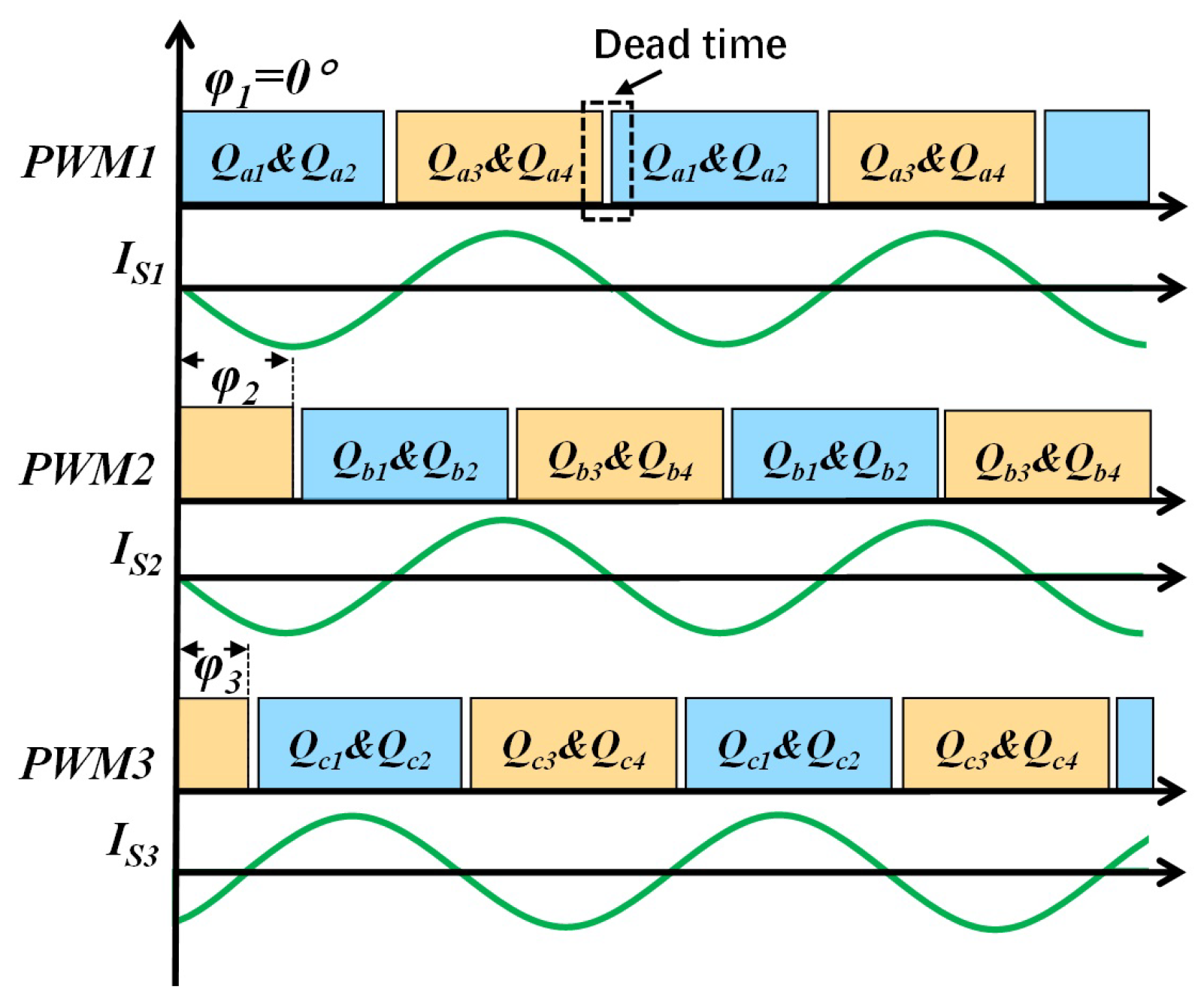
Figure 5 illustrates the switching sequence and key waveforms for the typical operating condition where the system supplies energy to port P 1 , relays energy to port P 2 , and outputs energy to port P 3 , with port P 1 connected to the power source, port P 2 connected to the energy storage load, and port P 3 connected to the resistive load. Here, φ 1 , φ 2 , and φ 3 represent the phase shift angles at ports P 1 , P 2 , and P 3 , respectively.

4.2. System Control Strategy

Based on the analysis of the three operating modes, the following conclusions are drawn: At port P 1 , the voltage and current are in anti-phase, indicating that it injects power into the LC resonant network. In port P 2 , the phase difference between voltage and current is 90 ° ; consequently, its average DC current is 0 A, and the active power is 0 W. Finally, port P 3 functions as a load terminal; as evidenced by the voltage-current phase relationship, it absorbs power from the LC resonant network.
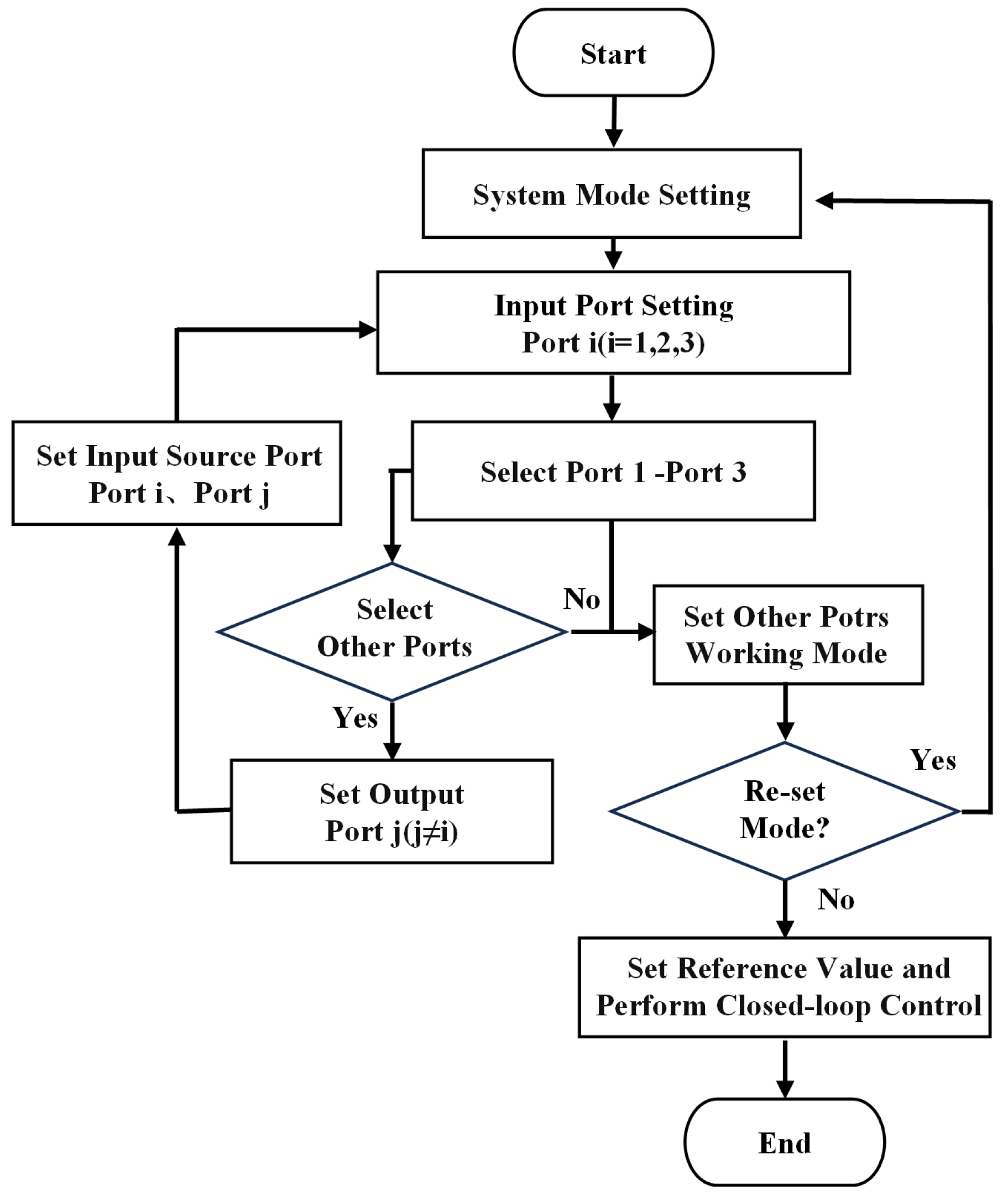
The system’s operational control strategy is illustrated in Figure 6. To avoid logic and power conflicts during mode switching, the system employs a mode preset mechanism: during initialization, it determines the mode of each port based on operating conditions (i.e., establishing the positions and quantities of source and load ends, along with their operational states) and sets reference parameters. Subsequently, it achieves precise mode switching and power flow control by dynamically adjusting the phase angles φ 1 to φ 3 in real time. When a power or load unit is taken out of service (e.g., due to depleted energy or load disconnection), the system automatically triggers a mode reconfiguration mechanism, redistributing port states, and entering a new steady-state control cycle.
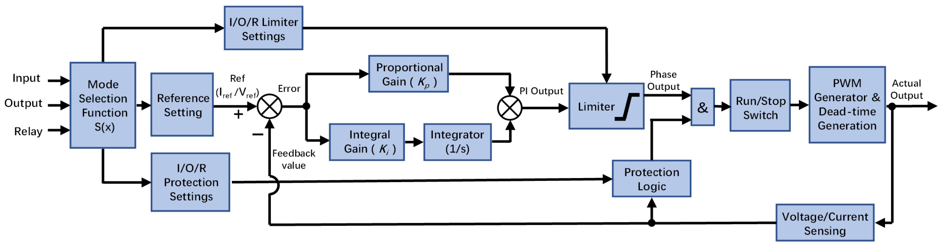
Figure 7 illustrates the real-time closed-loop control logic of the system following the completion of mode presetting. The control architecture primarily comprises three components: Mode Selection, Proportional–Integral (PI) Regulation, and Protection Logic. Initially, the Mode Selection Function module adaptively initializes the Reference Settings, Limiter Settings, and protection parameters based on the current port state (Input, Output, or Relay).
In the control loop, the error signal is derived by comparing the real-time feedback value (acquired by the voltage/current sensing module) with the reference value. This error signal is then processed by a PI controller. The controller’s output passes through a limiter to generate a preliminary phase control signal. Finally, this signal undergoes validation by the protection logic (implemented via AND logic or a Run/Stop Switch) and drives the PWM Generator only when the system operates in a fault-free state.
A conventional PI controller is adopted for the closed-loop control of the port output. The expression is given by:
C s = K p + K i s
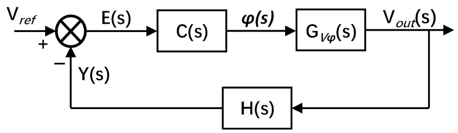
The closed-loop control block diagram of the port is shown in Figure 8. In this diagram, G V φ ( s ) represents the transfer function from the phase shift angle to the port output voltage, and H ( s ) denotes the transfer function of the voltage sensing network. Additionally, V r e f is the system reference voltage, Y ( s ) is the sampled feedback signal, E ( s ) represents the error signal between the reference and feedback values, and φ ( s ) denotes the phase control signal generated by the PI controller.
For the port input resistance R L i , by introducing small-signal perturbations around the steady-state operating point ( V o , i , Φ i , I i ) , the linearized small-signal equations are obtained as:
C f i d v ^ o , i d t = i ¯ i φ i φ ^ i + i ¯ i v o , i v ^ o , i v ^ o , i R L i
Applying the Laplace transform and rearranging the equation results in the control-to-output transfer function G v φ ( s ) :
G v φ ( s ) = v ^ o , i ( s ) φ ^ i ( s ) = K φ s C i + 1 R L i
where K φ = i ¯ i / φ i denotes the small-signal current gain with respect to the phase shift:
K φ = 8 V 1 π 2 S c o s sin φ i 0
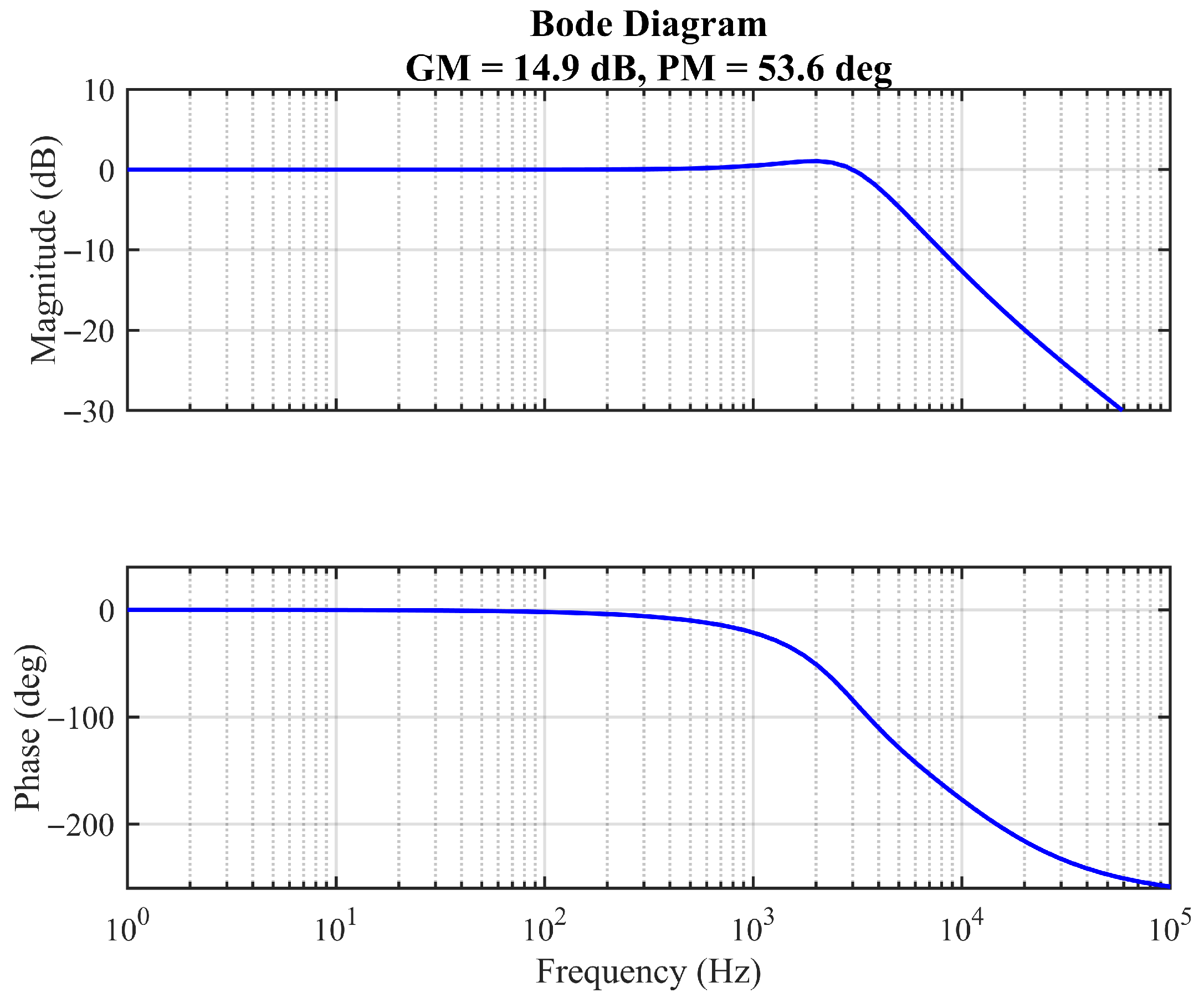
By substituting the system parameters into the transfer function G V φ s , the open-loop and closed-loop transfer functions are obtained. The corresponding Bode plot is generated using MATLAB R2023a, as shown in Figure 9. The system exhibits a crossover frequency of 4.5 kHz and a phase margin of 53.6°, which satisfies the stability criteria. Consequently, the closed-loop system is capable of stable operation.

5. System Simulation and Experimental Results

5.1. Simulation Results from the PSIM Platform

In order to verify the performance of the proposed system topology and the effectiveness of the control strategy, this paper constructs an open/closed-loop simulation model of the system based on the PSIM simulation platform, in which port P 1 is connected to a DC source, port P 2 is connected to different types of loads, and port P 3 is connected to a resistive load with a size of 10 Ω . The three operating states of the ports, namely, input, output, and relay, are verified using port P 2 as an example. The simulation and verification process is divided into two main stages: the first stage carries out the open-loop system characteristic scanning of the phase characteristics of port P 2 under different loads, to explore the power transfer boundary and the monotonic interval of the transfer characteristics of the system, and to provide data reference for the design of the closed-loop control limits; the second stage carries out the closed-loop control system validation of port P 2 in order to assess the dynamic response and steady-state performance of the system. The key simulation parameters are summarized in Table 1.

5.1.1. Open-Loop Scanning

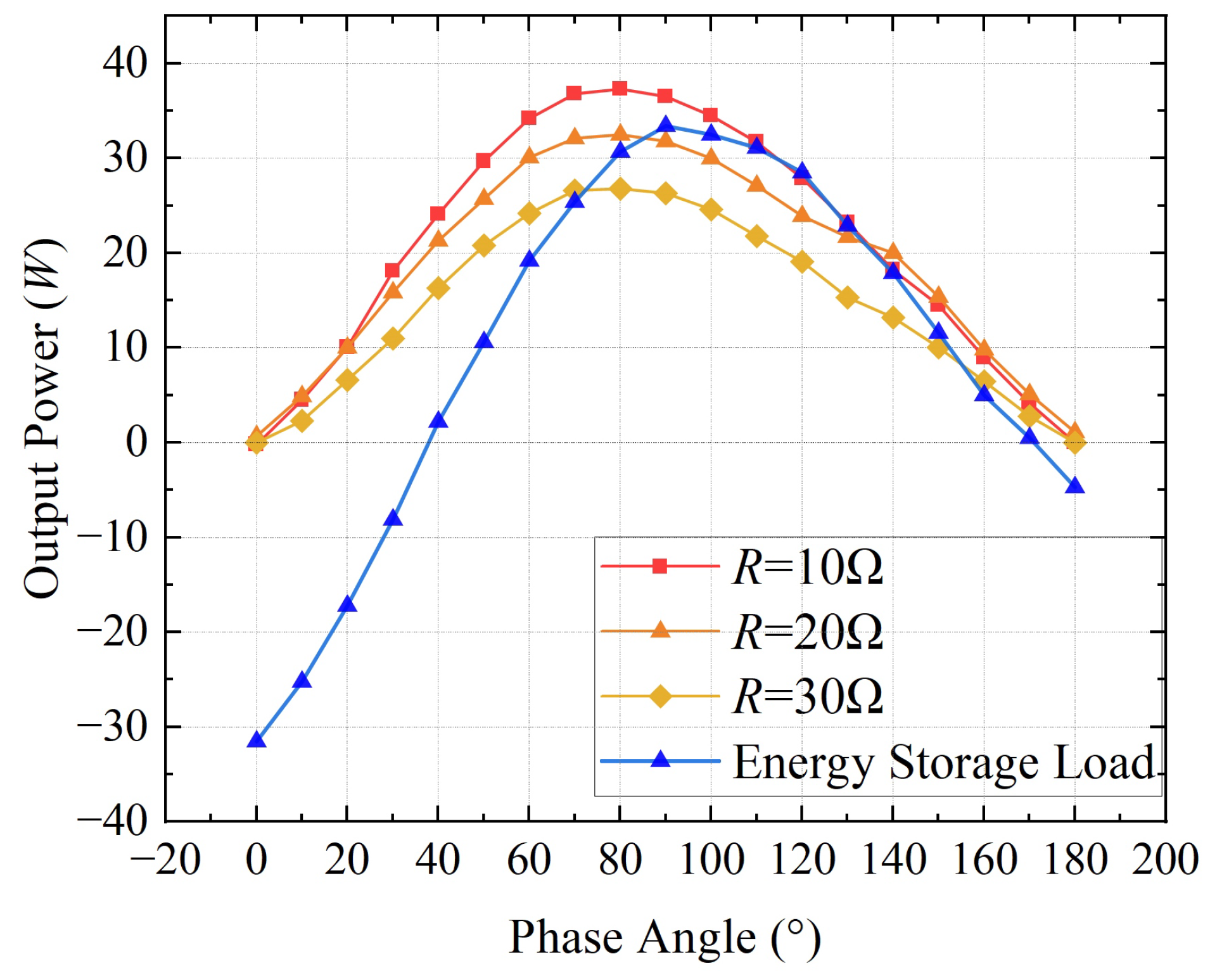
Figure 10 shows the results of open-loop scanning experiments with port P 2 connected to different resistance resistors and 24 V energy storage loads, in which the phase shift angle φ 2 varies from 0 ° to 180 ° (in steps of 10°).
Resistive Load Condition: When port P 2 is connected to a resistive load ( 10 Ω , 20 Ω ,   30 Ω , respectively), the output power shows unidirectional energy output characteristics and decreases with increasing resistance. The port output power shows an increasing and then decreasing trend with increasing phase shift angle: it increases monotonically from 0 ° to 80°, peaks at 80 ° , and finally decays to 0 W near 180 ° .
Energy storage load conditions: the system exhibits significant bi-directional power flow characteristics:
1.
Input Mode ( 0 ° < φ 2 < 40 ° ): Port power is negative (minimum about −32 W), indicating that at this time port P 2 acts as an energy input port, injecting energy into the resonant network and is in a discharged state.
2.
Relay Mode ( φ 2 40 ° , φ 2 180 ° ): Port power is 0 W, and the average current of the input and output of the port is 0A at the zero crossing point of the open-loop scanning curve, and the system is at the critical equilibrium point of energy exchange.
3.
Output Mode ( 40 ° < φ 2 < 180 ° ): Port power is positive, absorbing energy from the resonant network, and power peaks around 100 ° (about 33 W) and then drops again.
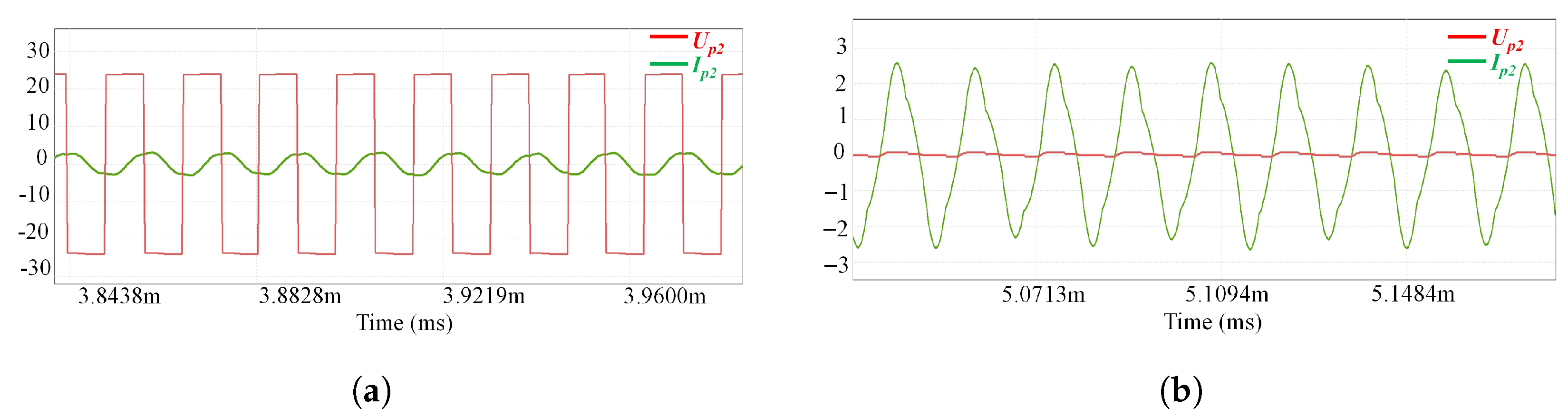
From the open-loop scanning results, when the input/output of port P 2 is 0 W, the port enters the relay mode and the relationship between its resonant current i S 2 and the full-bridge voltage u S 2 is shown in Figure 11.
Figure 11a shows the steady-state waveform in the case of the port P 2 energy storage load, the phase difference between the resonant current i S 2 of the port and the full-bridge voltage u S 2 is 90° in this mode, and the power injected/absorbed by the port into the resonant network is 0 W.
Figure 11b demonstrates the steady-state waveform in the case of port P 2 being connected to a resistive load (the size of the resistive load is 10 Ω ). The resonant current i S 2 of the port in this mode only participates in relaying the energy, and at this time the magnitude of the full-bridge voltage u S 2 is 0 V because the port is in relay mode.

5.1.2. Closed-Loop Verification Under PSIM

To evaluate the proposed control system in terms of dynamic mode switching and control performance, two simulation studies were conducted. Case I assesses the closed-loop power regulation capability and transient response speed of port P 2 . Case II emulates a transition of port P 2 from power-output mode to relay mode to verify the failure-rejection capability of the system.
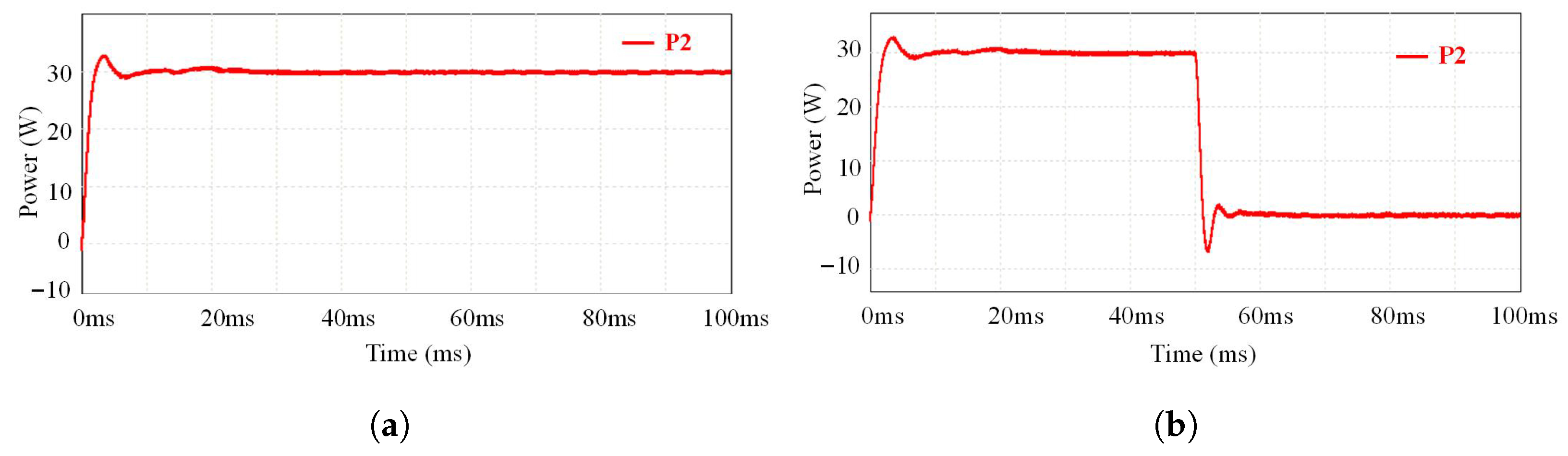
The dynamic response waveforms of the two experiments are illustrated in Figure 12a,b, respectively.
Figure 12a (Response to Closed-loop in output mode): The reference value is set to 30 W . Upon startup, the system tracks the command rapidly. After experiencing an overshoot of approximately 5 W , the system suppresses fluctuations via closed-loop regulation, settles within approximately 20 ms , and stabilizes at the rated power, thus achieving zero steady-state error.
Figure 12b (Response of the output-to-relay transition): The switching command is executed at t = 50 ms . Although a brief power outage (approximately 6 W ) occurs during the transient, the power rapidly returns and stabilizes at 0 W (relay state) within 30 ms under regulation. This validates the speed and smoothness of the system’s switching between different operating modes.
In summary, the simulation results validate the effectiveness of the proposed control strategy. The strategy not only provides accurate steady-state power regulation (see Figure 12a) but also enables flexible reconfiguration among multiple operating modes (see Figure 12b), thereby ensuring stable operation and high control accuracy of the multi-port wireless power transfer system under complex conditions.

5.2. Experimental Results

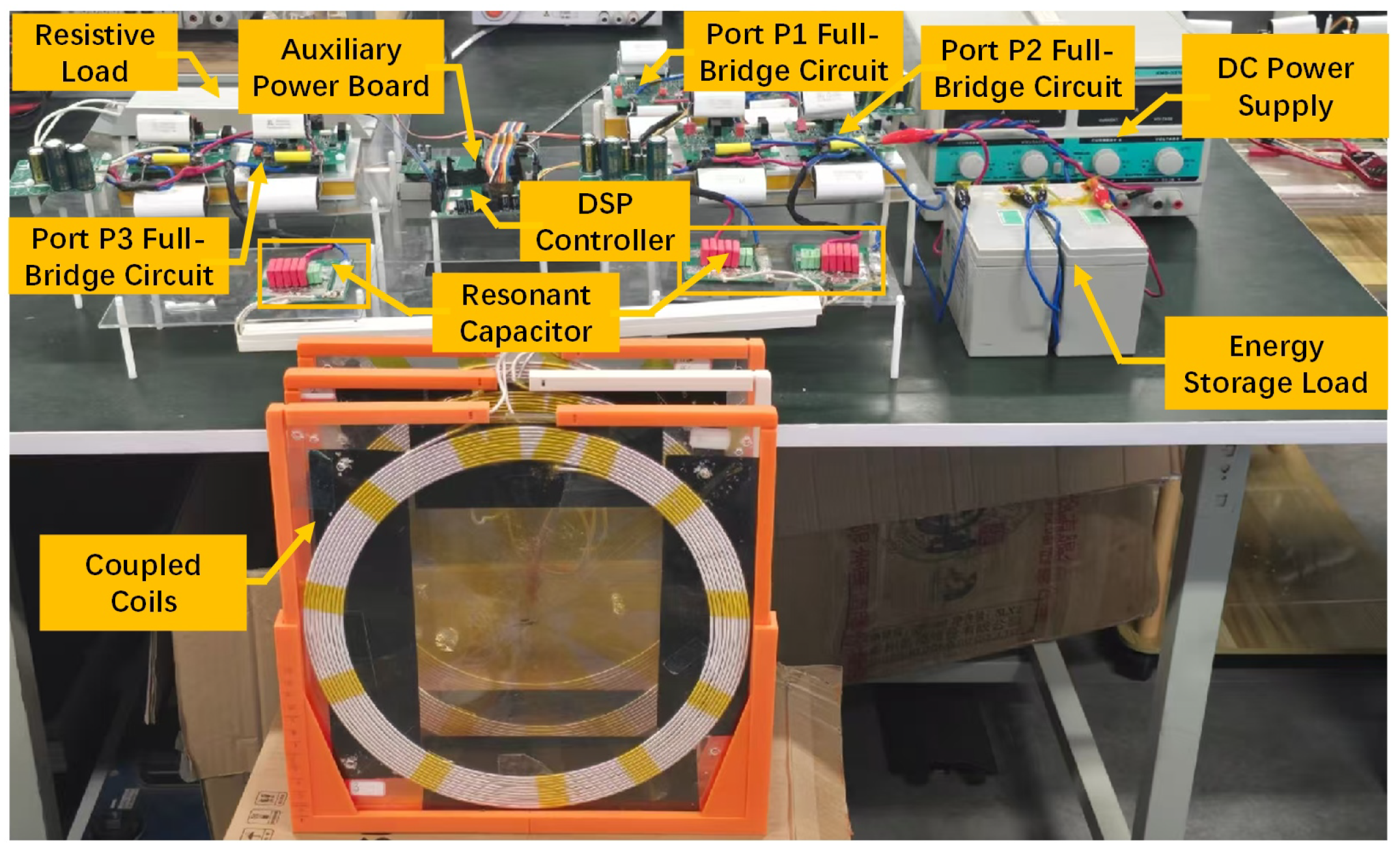
In order to verify the validity of the theoretical analysis and the mode switching of the system ports, a three-port multi-coil wireless energy transmission experimental platform was constructed (shown in Figure 13). The platform aims to verify the operating characteristics of the ports in the input, relay, and output modes. The dsPIC33FJ64GS606 is used as the control core, and the system is powered by a DC power supply and equipped with a 24 V battery pack and a power resistor to simulate different working conditions. The key system parameters are summarized in Table 2.

5.2.1. System Mode Validation Experiments

Based on the analysis of the open-loop scanning results of the simulation, it can be seen that the port has three modes, input, output, and relay, when connected to energy storage loads, while only output and relay modes are supported when connected to resistive loads. In the experiments, port P 1 (connected to a DC source) is designated as the power-input port. First, P 2 is connected to an energy-storage load and P 3 to a resistive load; then the three operating modes of P 2 are validated by adjusting the phase shift angle. Next, the load in P 2 is replaced with a resistive load to further evaluate its performance in the relay mode.
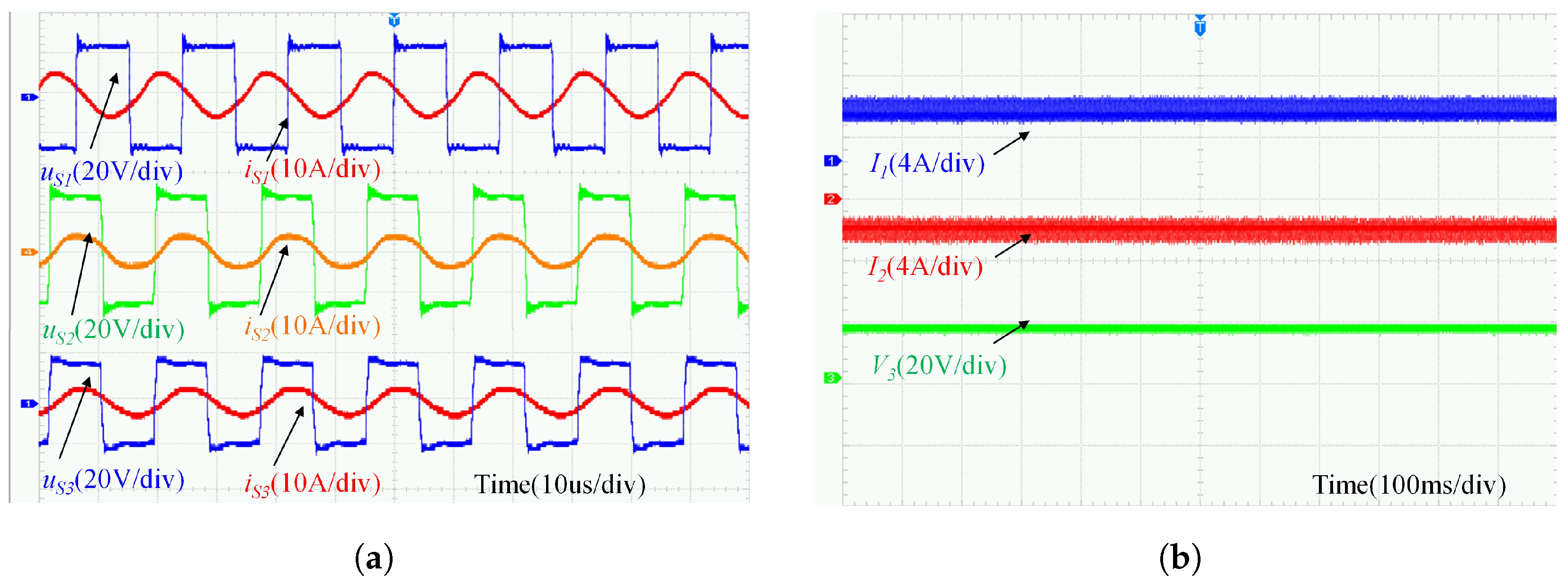
Figure 14 shows the steady-state waveforms and output characteristics when port P 1 is used as a single input source (DC 24 V) to supply power to ports P 2 and P 3 simultaneously. In the experiment, port P 2 is connected to a battery (energy storage load) and port P 3 is connected to a resistor (constant load).
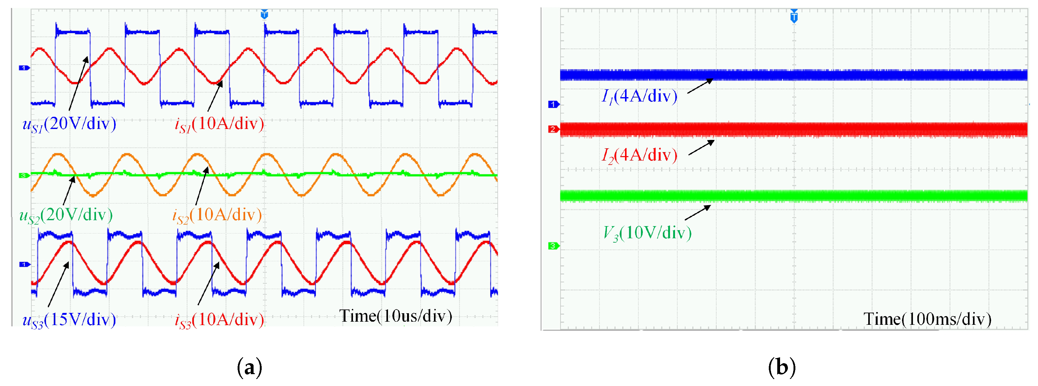
Figure 14a presents the steady-state operating waveforms of the full-bridge voltage ( u S 1 u S 3 ) and resonant current ( i S 1 i S 3 ) at each port. The system distributes power through phase-shift control, where the phase-shift angles in this mode are configured as φ 1 = 0 ° , φ 2 = 90 ° and φ 3 = 90 ° . Figure 14b shows the output characteristics of each port: port P 1 inputs 91.2 W (input current I 1 3.9 A); port P 2 outputs 50.1 W (output current I 2 of −2.1 A); and port P 3 outputs 25.5 W (output voltage V 3 of 16 V). The overall efficiency of the system is 83.1 % .
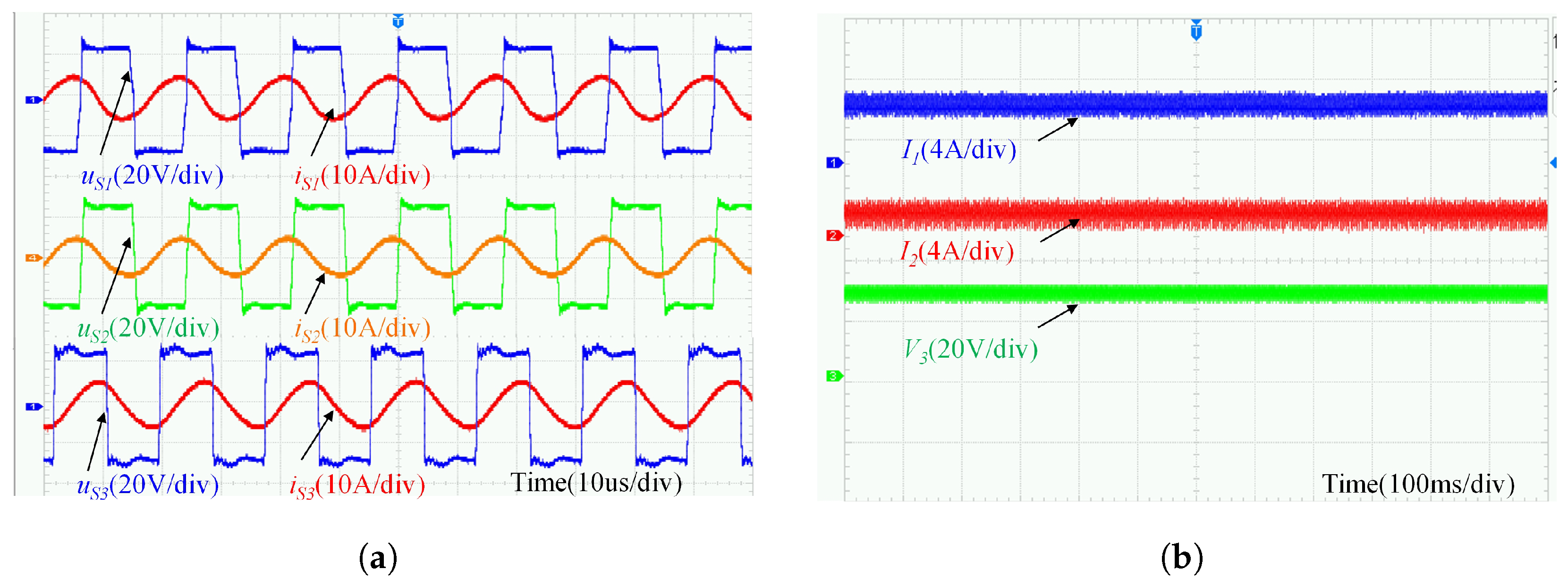
By adjusting the full-bridge phase φ 2 of port P 2 to 0 ° , port P 2 enters the input mode and the battery pack enters the discharge state. At this time, the system operates in the dual-input single-output mode, and energy is supplied to port P 3 by ports P 1 and P 2 together.
Figure 15a,b show the steady-state waveforms and output characteristics in this mode: the phase relationships of the full-bridge voltages u S 1 , u S 2 , and u S 3 between the ports are φ 1 = 0 ° , φ 2 = 0 ° and φ 3 = 90 ° , and the input powers of the ports P 1 and P 2 are 46.1 W (input current I 1 of 1.92 A) and 41.7 W ((input current I 2 of 1.74 A). Port P 3 outputs 71.8 W (output voltage V 3 of 26.8 V), giving an overall system efficiency of 81.5 % .
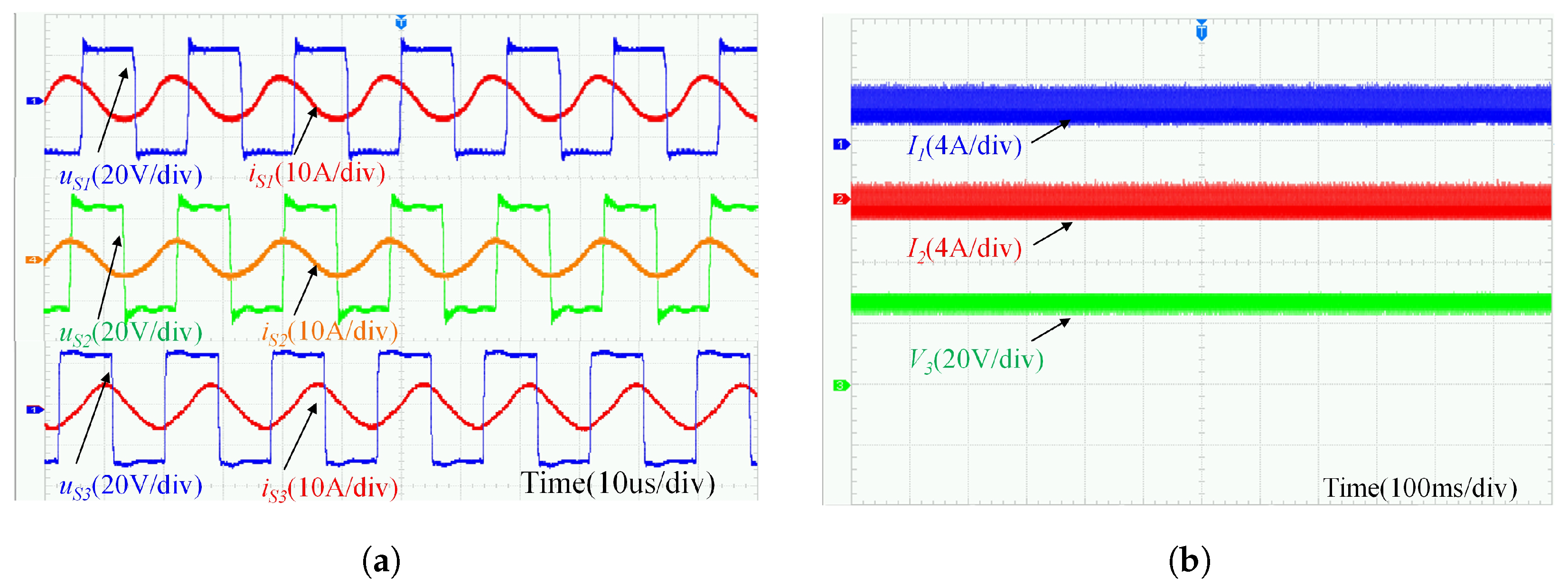
Figure 16 shows the experimental waveforms of port P 2 in relay mode. In this working condition, port P 1 transmits energy to port P 3 in one direction and port P 2 enters the operation in relay mode. The full-bridge voltage u S 2 of port P 2 exhibits a phase relationship 90 ° with the resonant current i S 2 , and the output current I 2 of the battery pack is kept near 0 A, i.e., the battery is neither charged nor discharged.
Figure 16a,b show steady-state waveforms and output characteristics in this mode, and the phase relationships of the full-bridge voltages u S 1 , u S 2 , and u S 3 between the ports are φ 1 = 0 ° , φ 2 = 35 ° , and φ 3 = 90 ° , respectively, and the output current I 2 of the battery pack is about 0 A. The input power of port P 1 is 72.5 W (input current I 1 of 3.02 A). The output power of port P 3 is 57.6 W (output voltage V 3 of 24.1 V). The overall efficiency of the system is 78.1 % .
Figure 17 shows the experimental waveforms of port P 2 connected to a resistive load in relay mode. In this operating condition, the output current i 2 of port P 2 is 0 A, and the corresponding load voltage is 0 V; however, a high-frequency resonant current i S 2 is maintained. Figure 17a,b illustrate steady-state waveforms and output characteristics in this mode. The phase angles of the full-bridge voltages ( u S 1 , u S 2 and u S 3 ) are configured as φ 1 = 0 ° , φ 2 = 5 ° and φ 3 = 90 ° , respectively. port P 1 supplies an input power of 26.4 W (input current I 1 of 1.1 A), while port P 3 delivers an output power of 19.4 W (output voltage V 3 of 13.8 V). The overall efficiency of the system is 73.4 % .
Based on the above experimental results, the component losses of the ports under different modes were analyzed and calculated, and the corresponding results are listed in Table 3.
In this experiment, the coils were wound using Litz wire, resulting in inevitable deviations in hardware parameters, which to some extent affected the overall system efficiency. In practical applications, the overall system efficiency can be further improved by employing coils fabricated with high-precision machining and winding processes, upgrading switching devices, and optimizing the LC network design.

5.2.2. Module Output Closed-Loop Control Experiment

To validate the effectiveness of the controller in regulating port modes, port P 1 was configured as a power input and connected to a 24 V DC power supply. The ports P 2 and P 3 were connected to a resistive load 10 Ω for power output. The closed-loop experiment comprised two parts: first, verifying the port’s steady-state regulation capability; second, testing the port’s dynamic response and disturbance rejection performance by varying the power command.
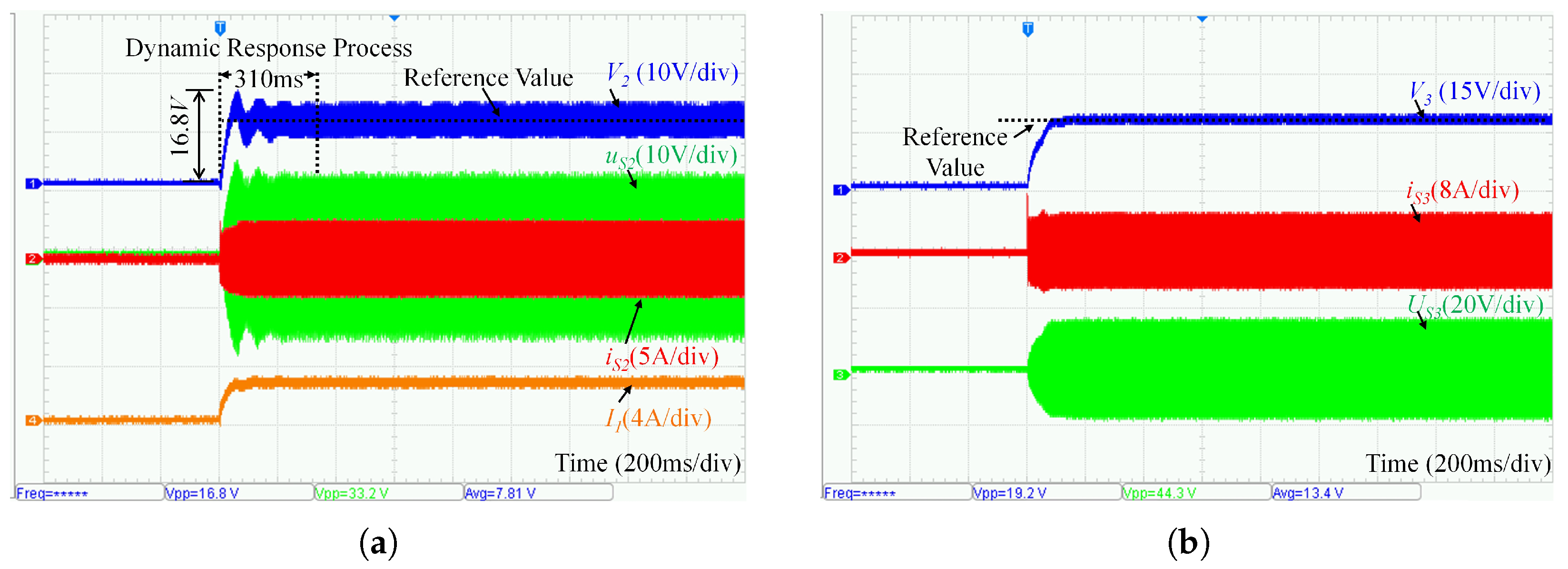
With the voltage references for port P 2 and port P 3 set at 15 V and 18 V, respectively, the steady-state experimental results are presented in Figure 18a,b.
Figure 18a displays the waveforms of the load voltage V 2 in port P 2 , the full-bridge voltage u S 2 , the resonant current i S 2 and the DC-side current I 1 in port P 1 . After system startup, the load voltage V 2 undergoes a brief overshoot (peaking at approximately 16.8 V), followed by a rapid controlled descent within 310 ms to stabilize near the 15.0 V reference value. Currently, the full-bridge output voltage u S 2 and the resonant current i S 2 also reach steady-state after a short adjustment period.
Figure 18b illustrates the process of regulating the load voltage V 3 at port P 3 , the full-bridge voltage u S 3 , and the resonant current i S 3 . After starting the system, the load voltage V 3 smoothly increases to 18 V, while the full-bridge output voltage u S 3 and the resonant current i S 3 enter synchronously steady state. These experimental results strongly validate the system’s excellent steady-state regulation capability.
The closed-loop experimental results demonstrate that the proposed system enables flexible power sharing and output regulation among multiple ports. Moreover, high control accuracy and satisfactory steady-state performance are achieved for the load currents, thereby validating the effectiveness of the designed controller.

5.2.3. Experimental Results of Port Operating-Mode Switching

To further validate the dynamic response characteristics and controller adjustment capabilities during system port mode switching, this paper conducts experiments on port P 2 . Modulation adjustment and switching are performed on module P 2 , with the experimental content divided into:
1.
Self-dynamic characteristic testing, covering power step responses and bidirectional switching between ‘output-relay’ modes;
2.
Cross-coupling characteristic testing, evaluating the impact of dynamic adjustments on port P 3 ’s response to P 2 . Dynamic characteristic testing of port P 2 itself.
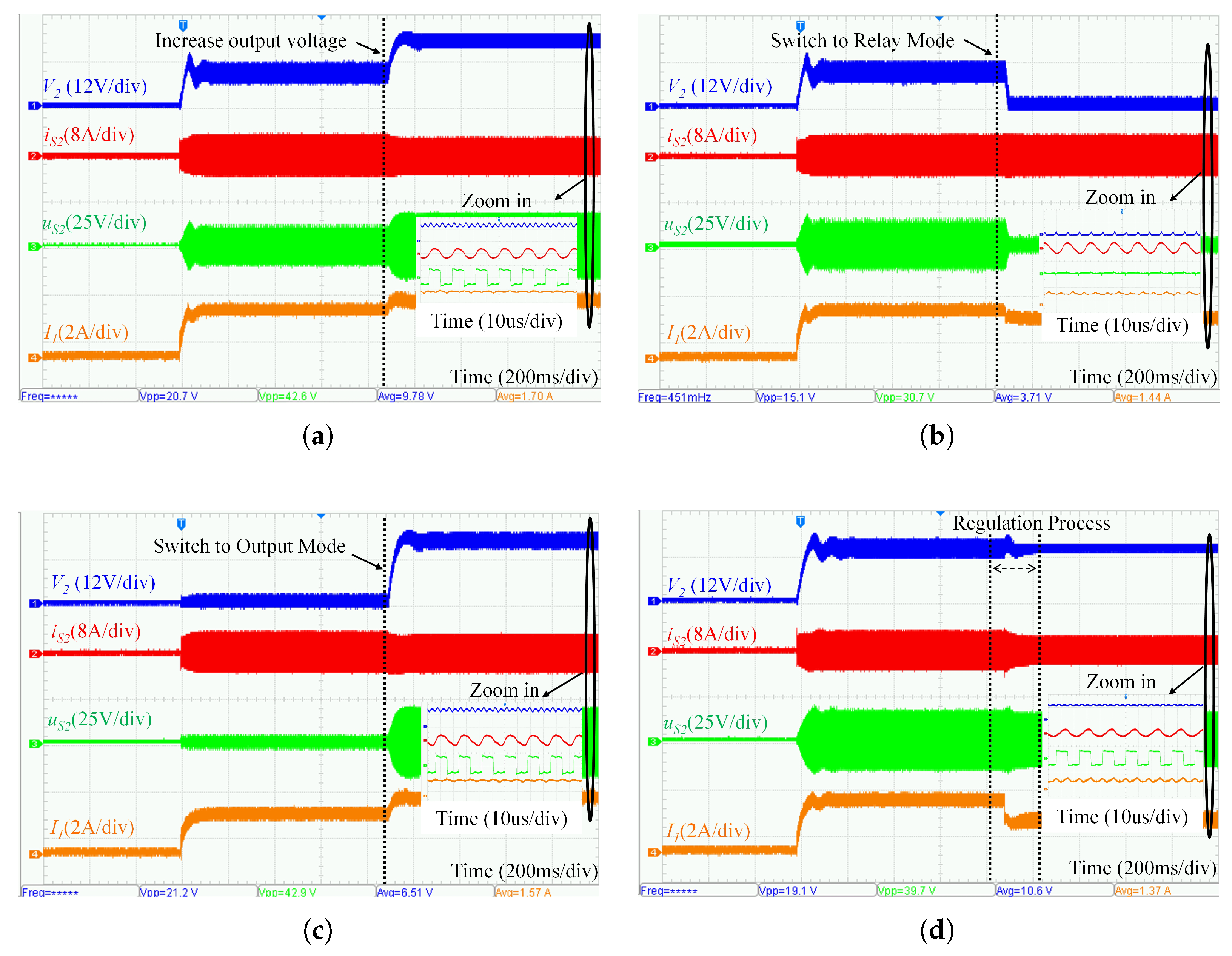
Figure 19 illustrates the dynamic response and corresponding steady-state waveforms under various mode switching conditions. Specifically, it displays the input current I 1 of port P 1 , as well as the output voltage V 2 , full-bridge output voltage u S 2 , and resonant current i S 2 of port P 2 .
Figure 19a depicts the system’s transition from startup to the initial steady state during an output power step-up experiment at port P 2 . Following system startup, the output voltage V 2 of port P 2 is maintained at 10 V, while the input current I 1 at port P 1 remains constant. At t = 0.8 s, the controller applies a step increase to the output voltage reference of port P 2 , raising it to 16 V. The waveforms indicate that the input current I 1 rises rapidly in response to the voltage command and stabilizes at a new operating point. Following this regulation, the full-bridge output voltage u S 2 and resonant current i S 2 of port P 2 re-establish steady-state characteristics. Ultimately, the input current I 1 settles at 2.5 A, with a settling time of approximately 200 ms.
Figure 19b illustrates the dynamic waveforms during the transition of port P 2 from Output Mode to Relay Mode. Initially, the system operates in steady state, with the output voltage V 2 of port P 2 maintained at 10 V. At t = 0.8 s, the mode switching command is executed. Consequently, V 2 drops rapidly to 0 V, accompanied by a synchronous reduction of the full-bridge output voltage u S 2 to 0 V. In contrast, the resonant tank current i S 2 exhibits a significant increase, while the input current I 1 at the source port P 1 decreases to 1.5 A. The transition time required for the system to complete this mode switch and establish a new steady state is approximately 100 ms.
Figure 19c illustrates the waveforms corresponding to the transition of port P 2 from Relay Mode back to Output Mode. After the system establishes the initial steady state, both the output voltage V 2 and the full-bridge output voltage u S 2 of port P 2 are 0 V, while the resonant current i S 2 is maintained at the level characteristic of relay operation. Upon triggering the switching command at t = 0.8 s , port P 2 initiates the mode transition. During this process, the resonant current i S 2 decreases compared to that in Relay Mode. Simultaneously, the output voltage V 2 stabilizes at approximately 15 V, accompanied by a synchronous rise in the full-bridge output voltage u S 2 . Furthermore, the input current I 1 at the port P 1 increases to 2.5 A. The entire mode switching process concludes with the restoration of steady state within approximately 200 ms.
Figure 19d presents the experimental results regarding the cross-coupling dynamic characteristics under multi-port cooperative operation, specifically verifying the impact of a sudden power drop at port P 3 port on P2. Upon reaching the initial steady state following system startup, the input current I 1 of port P 1 is 2.0 A, and the output voltage V 2 of port P 2 is 14 V. At t = 0.8 s , a step-down in output power is initiated at port P 3 . Consequently, the input current I 1 of port P 1 decreases to 1.2 A. Simultaneously, the controller regulates port P 2 to suppress the cross-coupling interference from port P 3 , thereby maintaining a stable output voltage. Following this regulation, the full-bridge output voltage u S 2 and resonant current i S 2 of port P 2 re-establish steady-state characteristics. The system fully recovers stable operation after a dynamic regulation period of approximately 200 ms.
In summary, the experimental results demonstrate that the proposed controller ensures stable operation and provides effective dynamic regulation under dynamic power-sharing and port mode transitions. The rapid attenuation of disturbances and the ability to maintain the desired output further confirm the fast transient response and high robustness of the proposed control strategy.
Table 4 presents the performance comparison between the proposed structure and previous related works.
Compared with other multi-port WPT systems, the structure proposed in this paper achieves bidirectional energy interaction while enabling the ports to operate in three modes: input, output, and relay. In contrast to other structures, the proposed control method is simpler, and the system requires fewer power devices and coils.

6. Conclusions

To address the challenges of energy interaction between modules and port mode adjustment in wireless multi-port systems, this paper proposes and validates a three-port wireless power transfer (WPT) system based on LC series resonance, along with its control strategy, successfully achieving inter-module energy interconnection and mode regulation at the load port. The mathematical model of the system and the small-signal model of the ports were established. By employing phase shift control based on a mode preset mechanism, power interaction among the three port modes—input, output, and relay—was realized. Based on the proposed strategy, an experimental prototype with a maximum transmission power of 100 W was built. The effectiveness of the control strategy was verified under different operating mode switching and cross-coupling conditions, achieving a regulation time of less than 200 ms and a maximum efficiency of 83.1 % . The results validated the seamless switching of ports and power flow control among multiple ports, while effectively extending the wireless energy transmission distance of the system. Furthermore, the component loss characteristics under each mode were analyzed in detail. It should be noted that this study was primarily conducted under fully aligned conditions, without fully considering the impact of coil misalignment and transmission distance variations. Future research will focus on analyzing system characteristics under misalignment and angular tilt, developing optimized control strategies, and mitigating port transient phenomena to further enhance system robustness.

Author Contributions

X.C.: Writing—review & editing, Writing—original draft, Conceptualization; Y.W.: Writing—review & editing, Writing—original draft; S.X.: Supervision, Software, Validation; P.N.: Formal analysis, Writing—review & editing; W.J.: Writing—review & editing; S.H.: Writing—review. All authors have read and agreed to the published version of the manuscript.

Funding

This work was supported by the Natural Science Foundation of the Jiangsu Higher Education Institutions of China (No. 24KJB470010).

Data Availability Statement

The original contributions presented in this study are included in the article. Further inquiries can be directed to the corresponding author.

Conflicts of Interest

The authors declare no conflicts of interest.

Appendix A

Analysis of Power Error under Fundamental Harmonic Approximation (FHA):
The series resonant network exhibits high impedance characteristics to high-frequency voltages. Under the condition of a load resistance R L = 10 Ω :
The equivalent AC resistance seen by the resonant tank is:
R a c = 8 π 2 R L 8.1 Ω
1. Impedance Calculation: At the fundamental frequency ( f 0 ): The impedance of the resonant tank is purely resistive:
Z 1 R a c = 8.1 Ω
At the 3rd harmonic frequency ( 3 f 0 ):
Z 3 = R a c 2 + X n e t 2 8 . 1 2 + 50 2 50.6 Ω
Similarly, at the 5th harmonic frequency ( 5 f 0 ):
Z 5 = R a c 2 + X n e t 5 2 = 8 . 11 2 + 90 . 27 2 90.63 Ω
2. Current Calculation (Assuming normalized fundamental voltage V 1 = 1 ): Fundamental current ( I 1 ):
I 1 = V 1 Z 1 = 1 8.11 0.1233
3rd harmonic current ( I 3 ):
I 3 = V 3 Z 3 = 1 / 3 50.83 0.0066
5th harmonic current ( I 5 ):
I 5 = V 5 Z 5 = 1 / 5 90.63 0.0022
3. Power Error Calculation:
The final power estimation error is calculated as follows:
Error P 3 + P 5 P 1 × 100 % = I 3 2 + I 5 2 I 1 2 × 100 %
Error I 3 2 + I 5 2 I 1 2 × 100 % 0 . 0066 2 + 0 . 0022 2 0 . 1233 2 × 100 % 0.32 %
Conclusion: The calculation demonstrates that the active power error caused by harmonic effects is approximately 0.32 % . Therefore, the FHA method provides a highly accurate estimation for this work.

References

  1. Alabsi, A.; Hawbani, A.; Wang, X.; Al-Dubai, A.; Hu, J.; Aziz, S.A.; Kumar, S.; Zhao, L.; Shvetsov, A.V.; Alsamhi, S.H. Wireless Power Transfer Technologies, Applications, and Future Trends: A Review. IEEE Trans. Sustain. Comput. 2025, 10, 1–17. [Google Scholar] [CrossRef] [Scilit]
  2. Lee, G.; Kim, M.Y.; Lee, S.G.; Kim, J.H. Operational Verification of Semidynamic Wireless Power Transfer in Light-Rail Transit Systems. IEEE Trans. Transp. Electrif. 2025, 11, 348–358. [Google Scholar] [CrossRef] [Scilit]
  3. Farghly, A.; Mohamed, A.; Awad, H.; Abdelfatah, S.; Alharbi, M.A.; Alqarni, M.; Ali Abdelrazik, S. A Comprehensive Review of Wireless Power Transfer Techniques for Electric Vehicle Charging. IEEE Access 2025, 13, 199683–199718. [Google Scholar] [CrossRef] [Scilit]
  4. Baros, D.; Voglitsis, D.; Papanikolaou, N.P.; Kyritsis, A.; Rigogiannis, N. Wireless Power Transfer for Distributed Energy Sources Exploitation in DC Microgrids. IEEE Trans. Sustain. Energy 2019, 10, 2039–2049. [Google Scholar] [CrossRef] [Scilit]
  5. Liu, Y.; Li, B.; Huang, M.; Chen, Z.; Zhang, X. An Overview of Regulation Topologies in Resonant Wireless Power Transfer Systems for Consumer Electronics or Bio-Implants. Energies 2018, 11, 1737. [Google Scholar] [CrossRef] [Scilit]
  6. Sun, S.; Zhang, B.; Rong, C.; Shu, X.; Wei, Z. A Multireceiver Wireless Power Transfer System Using Self-Oscillating Source Composed of Zero-Voltage Switching Full-Bridge Inverter. IEEE Trans. Ind. Electron. 2022, 69, 2885–2895. [Google Scholar] [CrossRef] [Scilit]
  7. Kim, S.; Covic, G.A.; Boys, J.T. Tripolar Pad for Inductive Power Transfer Systems for EV Charging. IEEE Trans. Power Electron. 2017, 32, 5045–5057. [Google Scholar] [CrossRef] [Scilit]
  8. Han, H.; Mao, Z.; Zhu, Q.; Su, M.; Hu, A.P. A 3D Wireless Charging Cylinder with Stable Rotating Magnetic Field for Multi-Load Application. IEEE Access 2019, 7, 35981–35997. [Google Scholar] [CrossRef] [Scilit]
  9. Imura, T.; Hori, Y. Maximizing Air Gap and Efficiency of Magnetic Resonant Coupling for Wireless Power Transfer Using Equivalent Circuit and Neumann Formula. IEEE Trans. Ind. Electron. 2011, 58, 4746–4752. [Google Scholar] [CrossRef] [Scilit]
  10. Ahn, D.; Hong, S. A Study on Magnetic Field Repeater in Wireless Power Transfer. IEEE Trans. Ind. Electron. 2013, 60, 360–371. [Google Scholar] [CrossRef] [Scilit]
  11. Cheng, C.; Lu, F.; Zhou, Z.; Li, W.; Deng, Z.; Li, F.; Mi, C. A Load-Independent LCC-Compensated Wireless Power Transfer System for Multiple Loads with a Compact Coupler Design. IEEE Trans. Ind. Electron. 2020, 67, 4507–4515. [Google Scholar] [CrossRef] [Scilit]
  12. Cheng, C.; Zhou, Z.; Li, W.; Deng, Z.; Mi, C.C. A Power Relay System with Multiple Loads Using Asymmetrical Coil Design. IEEE Trans. Ind. Electron. 2021, 68, 1188–1196. [Google Scholar] [CrossRef] [Scilit]
  13. Hou, X.; Wang, Z.; Su, Y.; Liu, Z.; Deng, Z. A Dual-Frequency Dual-Load Multirelay Magnetic Coupling Wireless Power Transfer System Using Shared Power Channel. IEEE Trans. Power Electron. 2022, 37, 15717–15727. [Google Scholar] [CrossRef] [Scilit]
  14. Liu, S.; Yan, X.; Xu, G.; Wang, G.; Liu, Y. An Eight-Coil Wireless Power Transfer Method for Improving the Coupling Tolerance Based on Uniform Magnetic Field. Processes 2024, 12, 2109. [Google Scholar] [CrossRef] [Scilit]
  15. Wang, H.; Cheng, K.W.E. Analysis, Design, and Validation of a Decoupled Double-Receiver Wireless Power Transfer System with Constant Voltage Outputs for Industrial Power Supplies. IEEE Trans. Ind. Inform. 2023, 19, 362–370. [Google Scholar] [CrossRef] [Scilit]
  16. Pan, W.; Xie, R.; Zhuang, Y.; Mao, X.; Zhang, Y. A Multi-Output Wireless Power Transfer System Based on Non-Overlapping Self-Decoupling Magnetic Couplers. IEEE Trans. Magn. 2024, 60, 1–5. [Google Scholar] [CrossRef] [Scilit]
  17. Li, Y.; Chu, X.; Li, Z.; Zhai, Y.; Qin, H. A Vertical Overlapping Decoupled Coil for Wireless Power Transfer With High Interoperability. IEEE Trans. Power Electron. 2025, 40, 16032–16041. [Google Scholar] [CrossRef] [Scilit]
  18. Wang, Y.; Sun, A.; Wang, F.; Liu, B. Analysis and Design of Wireless Bidirectional Power and Data Transfer With Decoupled DD-R Coil Geometry. IEEE Trans. Transp. Electrif. 2024, 10, 4709–4721. [Google Scholar] [CrossRef] [Scilit]
  19. Zhang, X.; Cai, T.; Duan, S.; Feng, H.; Hu, H.; Niu, J.; Chen, C. A Control Strategy for Efficiency Optimization and Wide ZVS Operation Range in Bidirectional Inductive Power Transfer System. IEEE Trans. Ind. Electron. 2019, 66, 5958–5969. [Google Scholar] [CrossRef] [Scilit]
  20. Jia, S.; Chen, C.; Duan, S.; Chao, Z. Dual-Side Asymmetrical Voltage-Cancelation Control for Bidirectional Inductive Power Transfer Systems. IEEE Trans. Ind. Electron. 2021, 68, 8061–8071. [Google Scholar] [CrossRef] [Scilit]
  21. Zhang, X.; Liu, F.; Lei, K.; Yu, S.; Yan, C. Three-Port Magnetically Coupling Resonant Wireless Energy Router and Its Zero-Power-Flow Control Scheme. In Proceedings of the IECON 2020 the 46th Annual Conference of the IEEE Industrial Electronics Society, Singapore, 18–21 October 2020; pp. 3936–3941. [Google Scholar]
  22. Cai, W.; Lai, X.; Ma, D.; Tang, H.; Hashmi, K.; Xu, J. Management of Multiple-Transmitter Multiple-Receiver Wireless Power Transfer Systems Using Improved Current Distribution Control Strategy. Electronics 2019, 8, 1160. [Google Scholar] [CrossRef] [Scilit]
  23. Liu, W.; Chau, K.T.; Lee, C.H.T.; Han, W.; Tian, X.; Lam, W.H. Full-Range Soft-Switching Pulse Frequency Modulated Wireless Power Transfer. IEEE Trans. Power Electron. 2020, 35, 6533–6547. [Google Scholar] [CrossRef] [Scilit]
  24. Zhou, M.; Liu, F.; Lu, K.; Chen, X. Modular Stacked Multiport Wireless Energy Interconnection System with Virtual AC Bus and Its Power Flow Control Strategy. IEEE Trans. Power Electron. 2022, 37, 15774–15784. [Google Scholar] [CrossRef] [Scilit]
  25. Xu, S.; Nie, P.; Jiang, W.; Hashimoto, S. Synthesis and Control of a Three-Port LCL Resonant Wireless Power Transfer System for DC Energy Conversion Applications. IEEE Trans. Power Electron. 2024, 39, 8916–8927. [Google Scholar] [CrossRef] [Scilit]
Figure 1. The proposed system framework diagram.
Symmetry 18 00447 g001
Figure 2. The proposed system topology.
Symmetry 18 00447 g002
Figure 3. Voltage and current waveforms of the resonant module.
Symmetry 18 00447 g003
Figure 4. Equivalent circuit diagram of the system.
Symmetry 18 00447 g004
Figure 5. Switching sequence and corresponding waveforms for different port operating states.
Symmetry 18 00447 g005
Figure 6. Port State Control Strategy Diagram.
Symmetry 18 00447 g006
Figure 7. Port Block diagram of the real-time closed-loop control logic.
Symmetry 18 00447 g007
Figure 8. Control block diagram.
Symmetry 18 00447 g008
Figure 9. Closed-loop system Bode diagram.
Symmetry 18 00447 g009
Figure 10. Open-loop scan results in input mode.
Symmetry 18 00447 g010
Figure 11. Waveform diagram of port P 2 in the steady state of the relay. (a) Relay mode waveform during energy storage load. (b) Relay mode waveform with resistive load.
Symmetry 18 00447 g011
Figure 12. Results of PSIM closed-loop simulation. (a) Closed-loop output regulation of the port. (b) Port P 2 transitions to relay mode.
Symmetry 18 00447 g012
Figure 13. Experimental platform.
Symmetry 18 00447 g013
Figure 14. Waveforms for the single-input dual-output operating condition. (a) Phase-shifted full-bridge waveforms of all ports in the system. (b) Output waveforms of the system ports.
Symmetry 18 00447 g014
Figure 15. Waveforms for the dual-input operation with a DC source and a battery. (a) Phase-shifted full-bridge waveforms of all ports in the system. (b) Output waveforms of the system ports.
Symmetry 18 00447 g015
Figure 16. Relay-mode output waveforms with port P 2 connected to an energy-storage load. (a) Phase-shifted full-bridge waveforms of all ports in the system. (b) Output waveforms of the system ports.
Symmetry 18 00447 g016
Figure 17. Relay-mode output waveforms with port P 2 connected to a resistive load (a) Phase-shifted full-bridge waveforms of all ports in the system. (b) Output waveforms of the system ports.
Symmetry 18 00447 g017
Figure 18. Output-control waveforms of the module. (a) Dynamic response of port P 2 . (b) Dynamic response of port P 3 .
Symmetry 18 00447 g018
Figure 19. Port operating-mode switching. (a) Dynamic response waveforms of port P 2 during an increase in output power. (b) Waveforms of port P 2 transitioning from output mode to relay mode. (c) Waveforms of port P 2 transitioning from relay mode to output mode. (d) Steady-state impact control of port P 2 under mode switching at port P 3 .
Symmetry 18 00447 g019
Table 1. System simulation parameters.
ParameterValue
Compensation Resonant Capacitance
C r 1 C r 3 155 nF
Compensation Resonant Inductance
L r 1 L r 3 54 μ H
System Operating Frequency55 kHz
Input Voltage24 V
Battery Voltage24 V
Table 2. System Experimental Parameters.
ParameterValue
Switching Frequency55 kHz
Coil Self-inductance L r 1 54.2 μ H
Coil Self-inductance L r 2 54.7 μ H
Coil Self-inductance L r 3 54.6 μ H
Resonant Capacitance C r 1 155 nF
Resonant Capacitance C r 2 155 nF
Resonant Capacitance C r 3 155 nF
Battery Pack Voltage24 V
Digital ControllerdsPIC33FJ64GS606
MOSFETHY3810 (180 A 100 V)
DC Power SupplyITECH-ITN2131
Resistive LoadRXLG-100W-10RJ
Table 3. Analysis of Component Losses Under Different Modes.
ModeSwitching
Loss
Conduction
Loss
Coil Copper
Loss
Capacitor
ESR
Total
Loss
Input0.14 W0.83 W3.45 W0.25 W4.67 W
Output0.22 W0.32 W1.26 W0.10 W1.90 W
Relay (Battery)0.22 W0.31 W1.24 W0.10 W1.87 W
Relay (Resistor)0 W0.42 W1.68 W0.13 W2.05 W
Table 4. Performance Comparison of the Structure with Previous Works.
Ref.StructureNo. of Power
Devices/Coils
Power/
Efficiency
No. of Port
Modes
Control
Method
[22]Unidirectional12, 380 W/87%1HPSC
[23]Unidirectional16, 4220 W (86.27%)1PFM
[24]Bidirectional8, 2150 W/80%2PWM + PSM
[25]Bidirectional16, 81 kW/78.5%2HPSC
ProposedBidirectional12, 3100 W/83.1%3PSC
Disclaimer/Publisher’s Note: The statements, opinions and data contained in all publications are solely those of the individual author(s) and contributor(s) and not of MDPI and/or the editor(s). MDPI and/or the editor(s) disclaim responsibility for any injury to people or property resulting from any ideas, methods, instructions or products referred to in the content.