Next Article in Journal
Coupling between Trigeminal-Induced Asymmetries in Locus Coeruleus Activity and Cognitive Performance
Next Article in Special Issue
Determination of Spinel Content in Cycled Li1.2Ni0.13Mn0.54Co0.13O2 Using Three-Dimensional Electron Diffraction and Precession Electron Diffraction
Previous Article in Journal
Pseudo Almost Automorphic Solutions for Stochastic Differential Equations Driven by Lévy Noise and Its Optimal Control
Previous Article in Special Issue
Comprehensive Study of Li+/Ni2+ Disorder in Ni-Rich NMCs Cathodes for Li-Ion Batteries
 
 
Correction published on 6 December 2021, see Symmetry 2021, 13(12), 2339.
Article

New Features in Crystal Orientation and Phase Mapping for Transmission Electron Microscopy

1
SIMAP, Grenoble INP, Université Grenoble Alpes, CNRS, 38000 Grenoble, France
2
Max-Planck-Institut für Eisenforschung GmbH, Max-Planck-Str. 1, 40237 Düsseldorf, Germany
3
MATEIS, INSA Lyon, Université Lyon I, CNRS UMR 5510, 69621 Villeurbanne, France
*
Author to whom correspondence should be addressed.
Symmetry 2021, 13(9), 1675; https://doi.org/10.3390/sym13091675
Submission received: 5 August 2021 / Revised: 8 September 2021 / Accepted: 9 September 2021 / Published: 11 September 2021 / Corrected: 6 December 2021
(This article belongs to the Special Issue Electron Diffraction and Structural Imaging)

Abstract

:
ACOM/TEM is an automated electron diffraction pattern indexing tool that enables the structure, phase and crystallographic orientation of materials to be routinely determined. The software package, which is part of ACOM/TEM, has substantially evolved over the last fifteen years and has pioneered numerous additional functions with the constant objective of improving its capabilities to make the tremendous amount of information contained in the diffraction patterns easily available to the user. Initially devoted to the analysis of local crystallographic texture, and as an alternative to both X-ray pole figure measurement and EBSD accessories for scanning electron microscopes, it has rapidly proven itself effective to distinguish multiple different phases contained within a given sample, including amorphous phases. Different strategies were developed to bypass the inherent limitations of transmission electron diffraction patterns, such as 180° ambiguities or the complexity of patterns produced from overlapping grains. Post processing algorithms have also been developed to improve the angular resolution and to increase the computing rate. The present paper aims to review some of these facilities. On-going works on 3D reconstruction are also introduced.

1. Introduction

Automated crystal orientation mapping tools (ACOM) are largely used in electron microscopy to quantitatively analyze grain size and crystallographic textures of materials at micron or sub-micron scales. Among them, electron backscatter diffraction (EBSD) attachments for scanning electron microscopes (SEM) are the most popular and benefit from long-standing improvements, today reaching impressive speeds and indexing qualities. Similar developments for transmission electron microscopes (TEM) are more recent and are continuously gaining interest from the community. As their ACOM/SEM counterparts, the ACOM/TEM tools scan a small probe over the area of interest and acquire the complete set of local diffraction patterns producing a 4D dataset. For TEM operators, the characterization procedure is deeply modified as the data is stored on a disk so that the majority of the analysis is performed off-line, by extracting the relevant signal out of the stack of ‘images’ collected on-line. In addition to the calculation of orientation or phase mapping, this offers the possibility to highlight structural features (grains, twins, precipitates, dislocations, boundaries, etc.) with additional facilities, such as the construction of virtual images (bright- and dark-field, or computer processed combined images) and correlation coefficient maps. Off-line analysis also permits the indexing parameters to be optimized or the data to be corrected by using cleaning tools as the ones available in EBSD software, with no extra line cost.
The ACOM/TEM approach considered here has given rise to a software plus hardware package, known as the ASTARTM tool, which has been described on different occasions [1,2]. Its main features are the use of precession electron diffraction (PED) to improve the quality of the acquired patterns and the pioneering introduction of the template matching strategy for rapid orientation and phase identification. It is composed of four dedicated numerical software programs devoted, respectively, to pattern acquisition, template generation, pattern indexing, and results analysis. This package has significantly evolved over fifteen years by introducing novel functions and user-friendly facilities that increase the possibilities to analyze challenging materials and extract faint information from the diffracting signal. Electron precession is generated with the Digistar equipment supplied by NanoMEGAS SPRL [3]. ASTAR was successfully applied to a wide range of systems, including energy storage materials [4,5], amorphous materials [6,7], and nanomaterials [8,9].
The main objective of the present paper is to review the most salient improvements and to highlight the capabilities, as well as the limitations, of the strategies incorporated, or to be incorporated, into ASTAR. The template matching strategy is detailed and commented on in Section 2. In Section 3, it is demonstrated that this strategy remains efficient even when the diffraction patterns are acquired with a low-resolution camera. Section 4 describes how the 180° ambiguity problem, inherently associated to transmission election diffraction, is corrected. The final section introduces the ongoing works on 3D reconstructions that requires the diffracting signatures of all the overlapping grains to be distinguished.

2. Template Matching: Practical Aspects

The diffraction patterns collected in the TEM under scanning mode on polycrystalline materials are typically very far from zone axis (ZA) and correspond to random cuts of the reciprocal lattice by the Ewald sphere. In this case, the classical procedure that consisted of recognizing ZA patterns by manual comparison with a limited number of charts can no longer be exploited. However, it can be extended numerically to any orientation by pre-computing all possible patterns for all orientations of all the phases expected in the sample. Each of these theoretical patterns, called templates, is cross correlated to each of the collected patterns and the template giving the best score is selected, providing the desired information at a given location on the sample.
The cross-correlation strategy, known as template matching, uses a correlation index which is calculated as:
Q i = j = 1 m P x j , y j T i x j , y j j = 1 m P 2 x j , y j j = 1 m T i 2 x j , y j
In this equation, the diffraction pattern is represented by the intensity function P(x,y) and every template i is given by the function Ti(x,y). The pattern and template contain m pixels but of interest is the fact that the template only has a limited number of non-zero pixels m′.

2.1. Algorithm Improvements

Indeed, template matching implies that only a small fraction of the pattern will match the template. In the current approach, the theoretical pattern does not reproduce the entire diffracting signal but only the most relevant part of it. More precisely, a template contains typically less than m′ ~ 100 datapoints Ti(x,y), each being representative of the position and the intensity of one reflection. This differs from a full cross-correlation approach where the entire simulated pattern is reproduced and compared to the raw data [10]. The processing time is tremendously reduced by considering such a minimal representation of the pattern. For example, even if the size of the collected pattern is not more than 144 × 144 pixels—the standard size used in the present approach—the number of operations in Equation (1) is reduced from m ~ 2.104 (total number of pixels) down to m′ ~ 100 (non-zero pixels in the template).
Additionally, the best match is related to the highest Q value for a given pattern. This means that the following equation would lead to exactly the same hierarchy and the same solution as Equation (1):
Q e f f i = j = 1 m P x j , y j T i x j , y j j = 1 m T i 2 x j , y j
Because the selection of the best template for a given diffraction pattern does not depend on the normalization of the pattern, this calculation is omitted to speed up the template matching process. The drawback of such a simplification is that the correlation index (Qeff) has an arbitrary value which is no longer bounded to a maximum score of 1. This results in an index score that is sensitive to the pattern brightness, but this has no impact on the results as each pattern is treated independently.
Templates are computed in a straightforward manner: the positions of the reflections are determined by a simple geometrical construction that depends on the lattice parameters and the Euler angles, whilst the template intensities are proportional to the square of the structure factor:
F h k l = i f i e 2 π i h x i + k y i + l z i
This requires the knowledge of the type and position of all atoms in the unit cell. The atomic scattering factor fi is approximated by the atomic number. Moreover, the intensity dependence on the Bragg angle is merely omitted. This choice reinforces the weight of the reflections appearing at the rim of the pattern, the ones that are more sensitive to the exact orientation of the crystal, therefore, increasing the angular resolution.

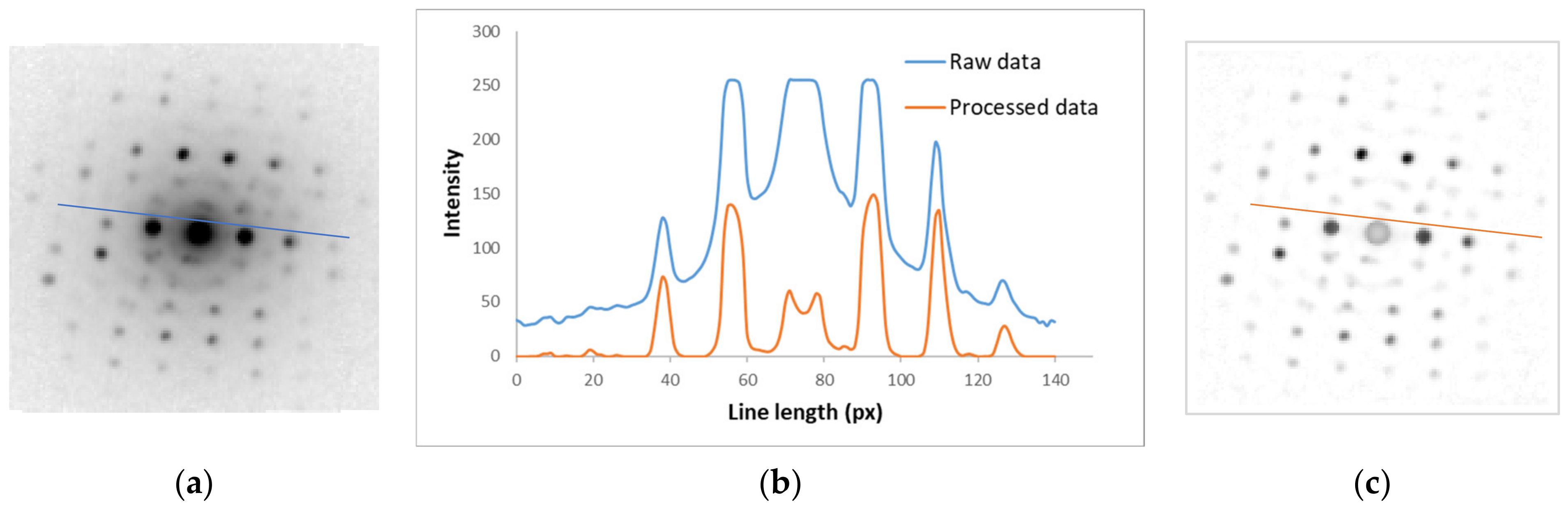
2.2. Background Subtraction
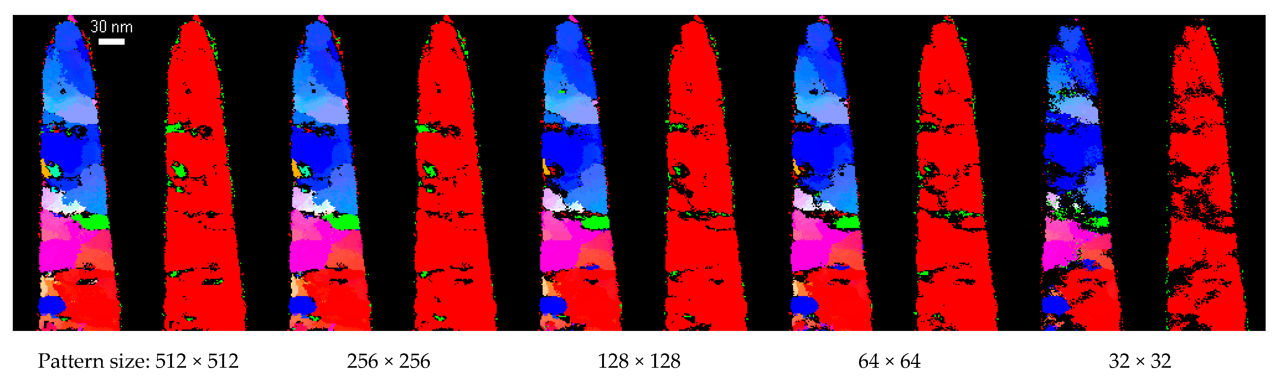
If no energy filter is used, the raw data displays a significant background intensity due to inelastically scattered electrons that increases when approaching the transmitted beam. Such background is weakly orientation or phase dependent but will produce a substantial contribution to the Q value for all templates whatever the location of the theoretical reflections. Therefore, it is necessary to eliminate it. This is performed by subtracting the local background intensity at every pixel in the pattern. In practice, this is calculated by averaging the intensity over a circle of a given radius drawn around the current position. The radius is ideally half the smallest distance existing between the reflections. Negative values produced by this calculation are subsequently set to zero. Consequently, the transformed pattern contains relative intensities that are far more appropriate for template matching (Figure 1).
Additional image processing steps may be used to further optimize the phase and/or orientation recognition. Experience has shown that a threshold of around 5% of the maximum intensity as well as a gamma correction of 0.5—enhancing intermediate intensities—usually improve the results.

3. Raw Pattern Size

As mentioned above, templates are crude estimates of the real diffraction patterns. They do not consider refined features like dynamical effects of the reflection profile and contain a very limited number of points. They may be considered as the diffraction pattern equivalent as minutiae for fingerprint representation. A precession angle of not more than 1° has proven very efficient to clean the pattern from strongly orientation-sensitive fluctuations (dynamical effects but also Kikuchi lines) [11]. Of interest is the fact that the orientation resolution is not bounded by the precession angle as long as the templates are corrected for precession [11,12,13].
In the standard procedure, the raw patterns are acquired on-line with an optical camera placed outside the TEM column. When scanning at high scan speeds, which may be hundreds of frames per second, the collected intensities are low such that binning (i.e., adding intensities of neighbouring pixels) is systematically performed. This substantially reduces the pattern resolution. The current trend in electron microscopy is to introduce new detectors which are faster and more sensitive but that also contain more pixels, up to several millions. While there is no doubt that orientation and phase mapping will benefit from these recent evolutions in hardware, this also comes with a tremendous increase in data size and acquisition time. To this respect, acquiring high resolution diffraction patterns is questionable, at least when templates are used to recognize the pattern. Figure 2 compares orientation and phase maps generated with patterns acquired with a 4k × 4k CMOS detector (TemCam-XF416-TVIPS) binned on-line to 512 × 512 pixels and further binned numerically to 256 × 256, 128 × 128, 64 × 64 and even 32 × 32 pixels for the sake of comparison.
The sample is extracted from a hypereutectoid pearlitic wire cold drawn to a true strain of ε = 6.02 and annealed for 2 min at 400 °C. Consequently, the ferritic grains contain substantial misorientations that are easily detected and even, surprisingly, for a reduction of the pattern resolution to just 32 × 32 pixels. At the lowest pattern resolutions, however, the ability to accurately identify intergranular cementite particles was lost. This is, however, an expected result as the distance between the closest reflections for Fe 3 C is smaller than for ferrite and are no longer distinguishable at the lowest resolutions.
Interestingly, both orientation and phase maps are practically identical for the as-collected data (512 × 512) and after a numerical binning down to 256 × 256 pixels. Even the embedded cementite particles are recognized despite the dominant diffracting signal from the ferrite matrix. This means that there is limited benefit from using a very large number of pixels. On the contrary, such results advocate for the use of a detector with large pixel sizes (i.e., higher intensities per pixel) rather than high resolutions. Notably, if large-pixel detectors (or binning) are used to reduce the exposure (and so experimental) time, there will be no substantial improvement in processing time with these lower resolution patterns, the latter being already highly optimized. Indeed, apart from the image processing time (e.g., background subtraction), the number of operations does not scale with the pattern resolution but with the subset m′ of datapoints contained in the templates, as discussed in Section 2.1.

4. Orientation Ambiguities

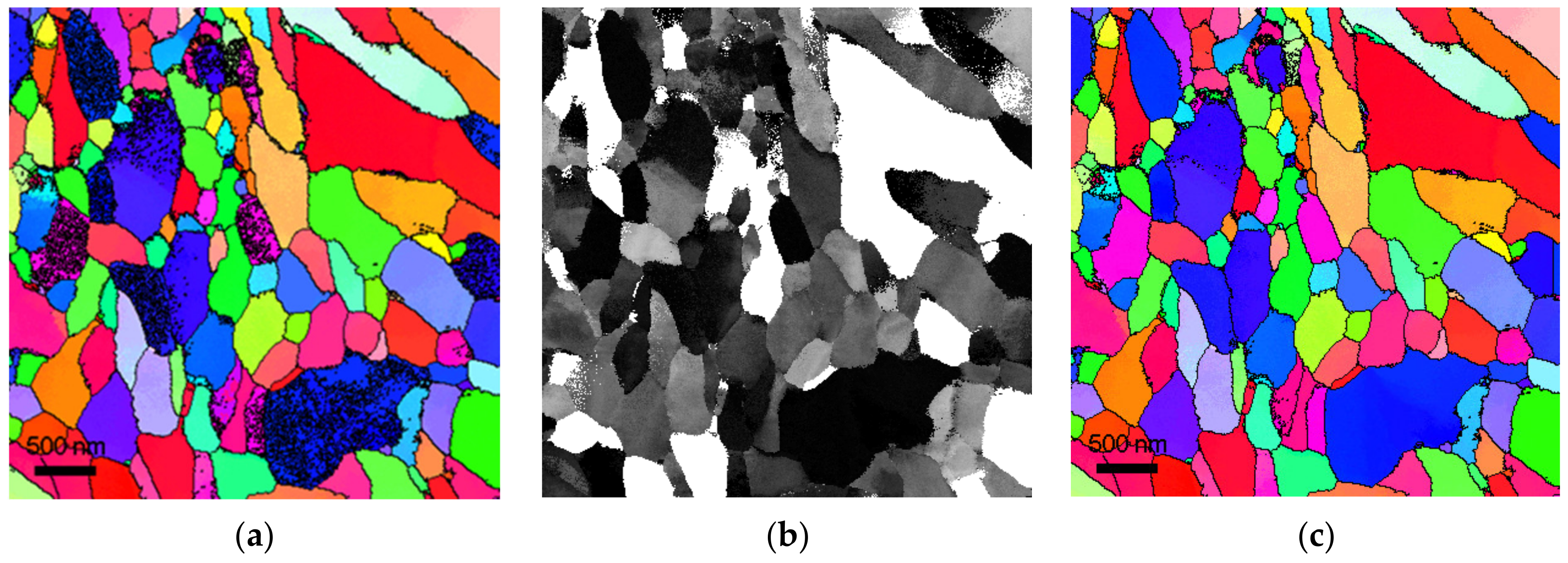
4.1. Detecting Ambiguities

One particular limitation of the ACOM/TEM approach that must be addressed is the famous 180° ambiguity problem. In transmission, the diffracting signal is limited to low Bragg angles, typically a few degrees. Consequently, the diffraction patterns may contain only the zero order Laue zone (ZOLZ) and the orientation determination is unsafe. A typical example is the {111} diffraction pattern for cubic materials whose ZOLZ exhibits a six-fold symmetry while the material has a three-fold symmetry. The absence of reflections belonging to a higher order Laue zone (HOLZ) prevents the crystal orientation from being distinguished between two possibilities that are related by a 180° rotation around the {111} ZA. This leads to possible misindexing and, consequently, damages the quality of the orientation maps and the reliability of the data.
A straightforward way to highlight orientation misindexing due to ambiguities is to draw the grain boundary map. Ambiguities will appear as spotty ‘boundaries’ within specific grains because misorientations related to the 180° rotation are higher than the threshold used to define a grain boundary (Figure 3a). Another characteristic signature of the induced error appears when the disorientations (minimum misorientation taking into account the symmetry of the crystal) measured along a line that crosses the area of interest is plotted: if the curve exhibits jumps of a few tens of degrees while the orientation is apparently unchanged (same color code) this is most probably related to a 180° ambiguity.
The capability of indexing software to handle such situations was questioned since the beginning of the development of ACOM/TEM approaches [14,15]. A specific workflow was developed to overcome the ambiguity issue and is described below.

4.2. Correcting Ambiguities

Highly symmetric diffraction patterns are intrinsically susceptible to ambiguities. If possible (single or multi-crystal), the sample should be tilted to avoid zone axes. If not (polycrystals), the missing information must be retrieved elsewhere. A possibility consists of extracting additional information from the local neighbourhood. Indeed, the orientation is never perfectly constant over a significant area: small orientation gradients are quite common because either the thin foil has a small curvature, or the material is intrinsically deformed. Consequently, a highly ambiguous spot pattern (i.e., highly symmetric) is surrounded by less problematic patterns. When detected, the ambiguity may be eliminated by extending the proper orientation from the most reliable points to the unreliable ones located in the close vicinity.
Therefore, a post-processing automated correction routine was developed. It consists of:
  • Calculating the local degree of ambiguity.
  • For ambiguous orientations, comparing the local orientation with that of neighbouring pixels.
  • Exchanging the orientation with the one corresponding to a 180° rotation around the closest zone axis. Of course, the ‘corrected’ orientation is kept only in the case of improvement (i.e., decrease of disorientation).
The degree of ambiguity is calculated through the template matching procedure: the selected template (Figure 4a) is tilted 180° around the ambiguity axis (Figure 4c) and the tilted template is compared to the acquired pattern (Figure 4b), producing a second value of the correlation index Q2. The related indexes (Q1 and Q2) are compared to give the ambiguity parameter:
Amb = 100 * (1 − Q2/Q1) (safe = 100, unsafe = 0),
Safe and unsafe grain may be noticed by plotting the ambiguity value in grey scale (Figure 3b). Notably, a rather confusing aspect of this construction is that a low value of the ‘ambiguity’ parameter means that the solution is highly ambiguous and vice-versa, i.e., it is perhaps better described as an ‘unambiguity’ parameter. The ambiguity axis around which this rotation should be performed is the closest ZA from the current orientation.
Practically, the orientation information is propagated from one pixel to the next, starting from the safest point with respect to ambiguities. Corrections are performed point by point with a random walking path that finally covers the whole area bounded by grain boundaries. As soon as a grain is completed, the process starts again for the remaining pixels, starting with the safest non-processed point, until the whole map is completed.
Figure 3 compares the results before (Figure 3a) and after (Figure 3c) the ambiguity correction for an iron polycrystal. For body cubic centred structures, <111> and <112> ZA are the most problematic (respectively, blue and pink for the present colour code).

5. Retrieving Through-Thickness Information

In transmission, the electron beam is, by definition, crossing the sample and when the sizes of the structural features are smaller than the thin foil thickness, it collects information from all the overlapping grains and phases. A standard template matching indexing procedure extracts the signature of the dominant grains of phases so that the resulting maps are not simple cross sections of the sample, as is the case for EBSD tools, for example. This drawback comes with an attractive opportunity: for the through-thickness information being collected, it must be possible to deconvolute the combined signatures to identify all the superimposed elements. There are several attempts to reconstruct the 3D crystal nature by relating automated crystal orientation and tilt series mapping [16,17,18]. Such an approach will be described in the last section. But the 4D dataset acquired in a single scan already contains 3D features that may be exploited. This is performed in the following section that makes use of both correlation coefficient maps [19] and multi-indexing [20].

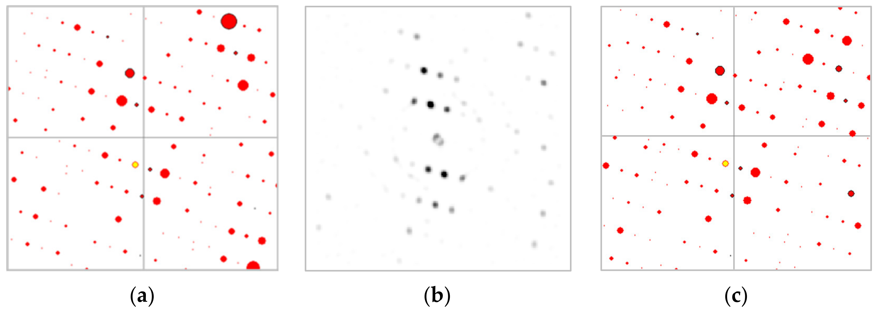
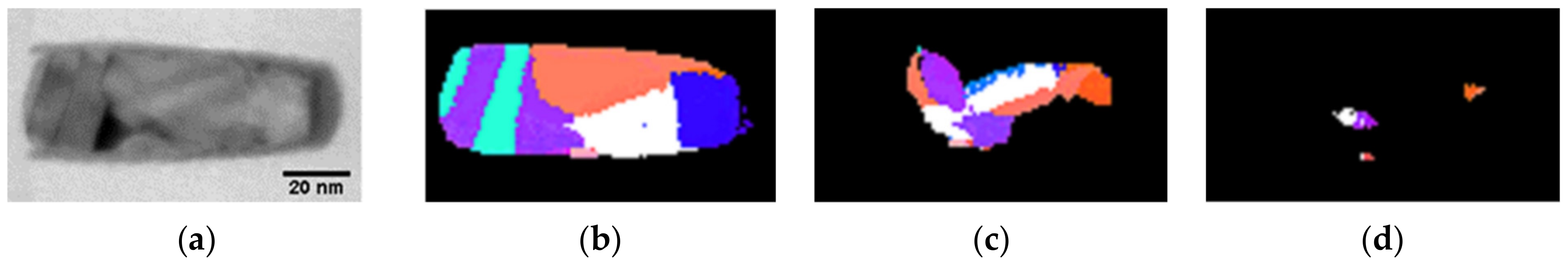
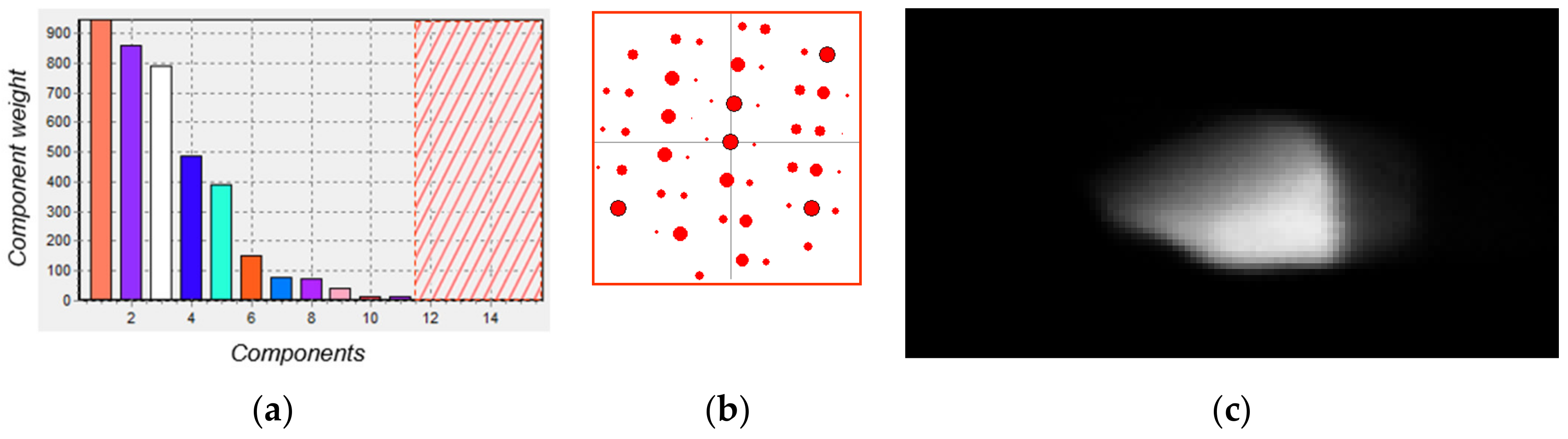
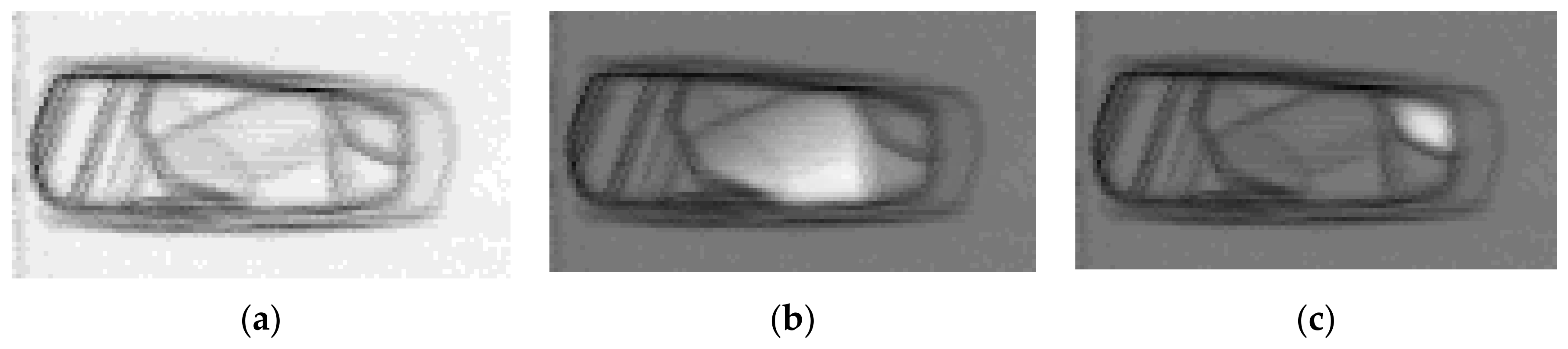
5.1. 3D Information Obtained from a Single Scan

With the template matching strategy, the acquired pattern is compared to all the pre-computed templates. The dominant one is retained but, in the case of overlapping crystals, additional candidates are also present. In order to recognize them properly, a good approach is to subtract the reflections related to the dominant grain before seeking for the next best match. The process, which may be repeated several times, is called multi-indexing and was described in detail elsewhere [20]. It may be used for orientation and phase identification [21,22].
The outcome of multi-indexing is a collection of all the orientations that were extracted either at the first or during the following indexations. The process is illustrated in Figure 5 for a copper nano device subjected three times to the multi-indexing procedure: it clearly shows that a given crystal is still detected after successive subtractions of the reflections related to the dominant grains.
A crystal exists if a non-negligible number of neighbor pixels have practically the same orientation. Consequently, the results are sorted into groups characterized by a limited orientation spread, typically 5°, and ranked by size (Figure 6a). As for a scree plot in principal component analysis, the smallest weights in the chart are related to noise or errors and thus the corresponding components are disregarded. As a side product of this procedure, the data is cleaned from misindexed components. The largest components are the constitutive crystals.
The grain orientation, defined either by an average over the component or by the orientation related to the highest correlation index for this particular grain, is associated to a unique template (Figure 6a). A second step consists of using this template as a mask for the construction of a combined virtual dark-field image [23], i.e., a numerical aperture that replicates the template is used to highlight the grain. The resulting ‘frozen template virtual dark-field’ (FTVDF) image reproduces the grain contour with, moreover, an intensity that is thickness dependent (Figure 6c).
The quality of the resulting image may be inferred by comparing it to the correlation coefficient map (CCM) [19,24]. The latter is a plot of the similarities between neighbouring diffraction patterns, calculated by a cross-correlation value, and highlights all material structural features that modify the diffracting conditions. The CCM looks similar to a projection of a semi-transparent sample and gives a direct view to 3D information, in particular the location and extent of grain boundaries (Figure 7a). The copper sample of Figure 5 contains numerous twins and the grain reconstructed in Figure 6c is bounded by an inclined twin boundary. As expected from the FTVDF image, the thickness of this crystal is at maximum in the lower part of the sample and vanishes in the upper part. This gradient is directly related to the inclined twin boundary shown in the CCM and illustrated by combining the two pictures in Figure 7b.
The same construction was used for all the components selected in Figure 6a. Of interest is the ‘hidden’ grain shown in Figure 7c that is clearly visible both in the CCM and in the FTVDF image but that was not detected through standard orientation mapping (a single indexing step, Figure 5b).
The capability to isolate grains from their surroundings provides a clear path towards 3D characterizations through tomographic reconstructions. The current state of such an attempt is described in the following section.

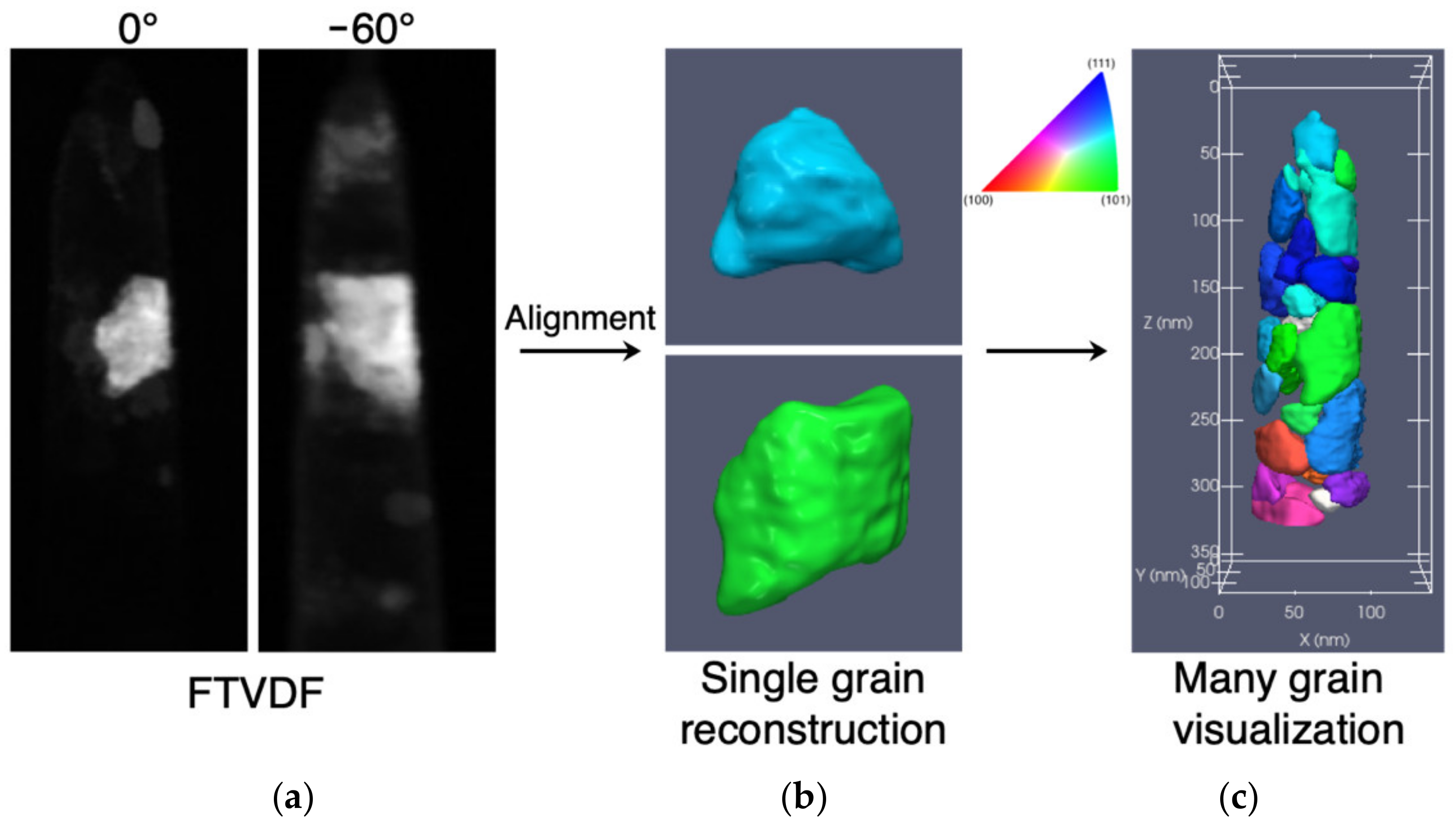
5.2. 3D Reconstruction from a Tilt Series

Despite the wealth of information contained within an orientation map, one of the main unknowns that remains is the complete 3D position of a grain within the sample. The in-plane (x, y) bounds of a grain are reasonably well defined, however, the z-position may be misinterpreted. It is common to believe that indexed grains within thin films are located at the same z-position, however when multiple grains exist within the projection this may not be the case. And whilst a better description of the volume of the grain can be calculated using FTVDF, as shown in the previous section, the z-ordering problem of overlapping grains still exists.
In order to more precisely determine the 3D position of grains within the sample, it is necessary to acquire images of the grains at different tilt angles (projections) within the TEM, a common practice in tomographic and stereographic imaging. Here, we will focus on tomographic reconstruction techniques from limited and restricted tilt experiments. Whilst the quality of tomographic reconstruction scales with the number of projections, from an experimental standpoint, this comes with the trade-off of experimental time on the TEM. The image acquisition time for direct imaging STEM (e.g., annular dark field) or TEM tomography experiments is typically on the order of seconds, whilst a single SPED dataset may take up to 30 min or more to acquire. This order of magnitude increase in frame acquisition time translates directly to experimental time. There may also be hardware-imposed limitations on the maximum achievable tilt angle. As a result, the microscope operator may wish to acquire datasets over a restricted tilt range, e.g., ±30°, at large tilt steps, e.g., 10°.
Three-dimensional reconstruction from electron nano-diffraction was performed by multiple groups using different reconstruction techniques [16,25]. Eggeman et al. reported on crystallographic analysis of a Ni superalloy imaged by scanning precession electron tomography and used non-negative matrix factorization to isolate diffraction patterns from different grains [16]. Meng et al. used VDF reconstructions to create projections of grains within a TiN sample suitable for tomographic reconstruction [25]. Here, we utilise the indexed grain orientation to create FTVDF images of individual grains at different projection angles for tomographic reconstruction. The virtual apertures are calculated from grain components using the multi-indexing technique and tracked through the experimental tilt series enabling virtual reconstruction from their diffraction signature [26].
To achieve this, the components calculated from the orientation map of each tilt dataset are ‘coupled’ together, i.e., the rotation R that maps component orientations O from tilt dataset i is calculated such that O i + 1 = R O i . Then, by choosing an initial grain orientation from a given dataset, FTVDF images highlighting the grain in this dataset and all related tilt datasets can be produced, i.e., projections of the grain.
This methodology also produces an additional benefit: the projections of any individual grain may be used for tilt series alignment. Fiducial marker alignment methods [27] are well suited to data where the same feature can be tracked through the entire tilt series. These methods are also able to correct for stretching and shearing image artefacts that may occur due to the long acquisition time of a SPED dataset and sample drift in the TEM. In fact, the issue that often arises where overlapping features in the image obfuscate the tracked feature of interest may be completely avoided using FTVDF reconstructions, as the grain of interest can be unambiguously highlighted.
Tomographic reconstruction of an individual, aligned grain created through FTVDF can then proceed through established tomographic reconstruction techniques (e.g., back projection, SIRT [28]). An example reconstruction for the cold-drawn pearlitic steel tip, presented in Figure 2, using the methods described here is shown in Figure 8. In this case, each grain was reconstructed individually into a common volume, including the cementite grains described previously in Figure 2. The material processing conditions were described in [29]. The ferritic grains are predominantly columnar in shape and extend through the sample depth in one dimension. In contrast, the cementite particles are more spherical, and the reconstruction shows their location within the tip volume. Using this reconstruction method, we were able to individually reconstruct grains of different phases where the smallest grains were ~20 nm in one or more dimensions.

6. Conclusions

Over the last fifteen years, the ACOM/TEM tool has proven as efficient and reliable towards the characterization of crystallographic orientations and phase distributions of crystallized materials, despite the physical constraints related to electron diffraction (dynamical effects, limited diffracting angles). The template matching algorithm detailed in this paper allows for rapid indexing and is effective even on low-resolution diffraction patterns. Numerous functionalities were implemented to improve the results; in particular, a dedicated functionality was implemented to solve the 180° ambiguity problem and a multi-indexing strategy was implemented to characterize the information within diffraction patterns superimposed by transmission of the electron beam through multiple grains. Moreover, the adaptability of the virtual reconstruction technique allows for the retrieval of some 3D spatial information from a single 2D dataset. By extending these techniques into 3D, e.g., scanning precession electron tomography, the full 3D description of grain shape and orientation may be calculated which creates the possibility to study grain relationships within the sample volume. This opens the door towards 3D characterization of complex nanomaterials and nano devices.

Author Contributions

Conceptualization, methodology, E.F.R., W.L. and M.H.; software, E.F.R. and P.H.; validation, E.F.R., P.H. and M.V.; formal analysis, E.F.R. and P.H.; investigation, E.F.R., X.Z. and P.H.; resources, E.F.R., M.H. and M.V.; writing—original draft preparation, E.F.R. and P.H.; writing—review and editing, E.F.R. and P.H.; visualization, E.F.R., X.Z. and P.H.; supervision, E.F.R., M.H. and M.V.; project administration, E.F.R.; funding acquisition, E.F.R., W.L., M.H. and M.V. All authors have read and agreed to the published version of the manuscript.

Funding

This research was partly funded by Agence National de la Recherche (ANR), grant number ANR-19-CE42-0017. M.H. acknowledges funding by the German Research Foundation (DFG) for funding via project HE 7225/11-1. The work has benefited from characterization equipment of the Grenoble INP-CMTC platform supported by the Centre of Excellence of Multifunctional Architectured Materials ‘CEMAM’ n°ANR-10-LABX-44-01 funded by the Investments for the Future programme.

Institutional Review Board Statement

Not applicable.

Informed Consent Statement

Not applicable.

Acknowledgments

We are grateful to Xuyang Zhou and Michael Herbig from MPIE at Düsseldorf (Germany) for their collaboration and particularly for supplying the steel raw data used to generate the results shown in Figure 2 and Figure 8.

Conflicts of Interest

The authors declare no conflict of interest.

References

  1. Rauch, E.F.; Véron, M. Automated Crystal Orientation and Phase Mapping in TEM. Mater. Charact. 2014, 98, 1–9. [Google Scholar] [CrossRef]
  2. Rauch, E.F.; Portillo, J.; Nicolopoulos, S.; Bultreys, D.; Rouvimov, S.; Moeck, P. Automated Nanocrystal Orientation and Phase Mapping in the Transmission Electron Microscope on the Basis of Precession Electron Diffraction. Z. Krist. 2010, 225, 103–109. [Google Scholar] [CrossRef] [Green Version]
  3. NanoMEGAS SPRL. Available online: https://nanomegas.com/ (accessed on 29 July 2021).
  4. Mu, X.; Kobler, A.; Wang, D.; Chakravadhanula, V.S.K.; Schlabach, S.; Szabó, D.V.; Norby, P.; Kübel, C. Comprehensive Analysis of TEM Methods for LiFePO4/FePO4 Phase Mapping: Spectroscopic Techniques (EFTEM, STEM-EELS) and STEM Diffraction Techniques (ACOM-TEM). Ultramicroscopy 2016, 170, 10–18. [Google Scholar] [CrossRef] [Green Version]
  5. Brunetti, G.; Robert, D.; Bayle-Guillemaud, P.; Rouvière, J.L.; Rauch, E.F.; Martin, J.F.; Colin, J.F.; Bertin, F.; Cayron, C. Confirmation of the Domino-Cascade Model by LiFePO4/FePO4 Precession Electron Diffraction. Chem. Mater. 2011, 23, 4515–4524. [Google Scholar] [CrossRef]
  6. Guo, W.; Meng, Y.; Zhang, X.; Bedekar, V.; Bei, H.; Hyde, S.; Guo, Q.; Thompson, G.B.; Shivpuri, R.; Zuo, J.; et al. Extremely Hard Amorphous-Crystalline Hybrid Steel Surface Produced by Deformation Induced Cementite Amorphization. Acta Mater. 2018, 152, 107–118. [Google Scholar] [CrossRef]
  7. Hart, M.J.; Bassiri, R.; Borisenko, K.B.; Véron, M.; Rauch, E.F.; Martin, I.W.; Rowan, S.; Fejer, M.M.; MacLaren, I. Medium Range Structural Order in Amorphous Tantala Spatially Resolved with Changes to Atomic Structure by Thermal Annealing. J. Non-Cryst. Solids 2016, 438, 10–17. [Google Scholar] [CrossRef]
  8. Santiago, U.; Velázquez-Salazar, J.J.; Sanchez, J.E.; Ruiz-Zepeda, F.; Ortega, J.E.; Reyes-Gasga, J.; Bazán-Díaz, L.; Betancourt, I.; Rauch, E.F.; Veron, M.; et al. A Stable Multiply Twinned Decahedral Gold Nanoparticle with a Barrel-like Shape. Surf. Sci. 2016, 644, 80–85. [Google Scholar] [CrossRef] [Green Version]
  9. Wang, Y.; He, J.; Mu, X.; Wang, D.; Zhang, B.; Shen, Y.; Lin, M.; Kübel, C.; Huang, Y.; Chen, H. Solution Growth of Ultralong Gold Nanohelices. ACS Nano 2017, 11, 5538–5546. [Google Scholar] [CrossRef]
  10. Wang, A.; Leff, A.C.; Taheri, M.L.; Graef, M.D. A Statistical Dictionary Approach to Automated Orientation Determination from Precession Electron Diffraction Patterns. Microsc. Microanal. 2015, 21, 1247–1248. [Google Scholar] [CrossRef] [Green Version]
  11. Nicolopoulos, S.; Bultreys, D.; Rauch, E. Precession Coupled Orientation/Phase Mapping on Nanomaterials with TEM Cs Microscopes. Acta Crystallogr. A Found. Crystallogr. 2012, 68, S104. [Google Scholar] [CrossRef] [Green Version]
  12. Rauch, E.F.; Véron, M. Crystal Orientation Angular Resolution with Precession Electron Diffraction. Microsc. Microanal. 2016, 22, 500–501. [Google Scholar] [CrossRef] [Green Version]
  13. Rauch, E.; Renou, G.; Veron, M. Reflection profile and angular resolution with Precession Electron Diffraction. In European Microscopy Congress 2016: Proceedings; Wiley-VCH Verlag GmbH & Co: Weinheim, Germany, 2016; pp. 665–666. ISBN 978-3-527-80846-5. [Google Scholar]
  14. Wu, G.; Zaefferer, S. Advances in TEM Orientation Microscopy by Combination of Dark-Field Conical Scanning and Improved Image Matching. Ultramicroscopy 2009, 109, 1317–1325. [Google Scholar] [CrossRef]
  15. Morawiec, A.; Bouzy, E. On the Reliability of Fully Automatic Indexing of Electron Diffraction Patterns Obtained in a Transmission Electron Microscope. J. Appl. Cryst. 2006, 39, 101–103. [Google Scholar] [CrossRef] [Green Version]
  16. Eggeman, A.S.; Krakow, R.; Midgley, P.A. Scanning Precession Electron Tomography for Three-Dimensional Nanoscale Orientation Imaging and Crystallographic Analysis. Nat. Commun. 2015, 6, 7267. [Google Scholar] [CrossRef] [PubMed] [Green Version]
  17. Kobler, A.; Kübel, C. Towards 3D Crystal Orientation Reconstruction Using Automated Crystal Orientation Mapping Transmission Electron Microscopy (ACOM-TEM). Beilstein J. Nanotechnol. 2018, 9, 602–607. [Google Scholar] [CrossRef] [PubMed]
  18. Liu, H.H.; Schmidt, S.; Poulsen, H.F.; Godfrey, A.; Liu, Z.Q.; Sharon, J.A.; Huang, X. Three-Dimensional Orientation Mapping in the Transmission Electron Microscope. Science 2011, 332, 833–834. [Google Scholar] [CrossRef] [PubMed] [Green Version]
  19. Kiss, Á.K.; Rauch, E.F.; Lábár, J.L. Highlighting Material Structure with Transmission Electron Diffraction Correlation Coefficient Maps. Ultramicroscopy 2016, 163, 31–37. [Google Scholar] [CrossRef]
  20. Valery, A.; Rauch, E.F.; Clément, L.; Lorut, F. Retrieving Overlapping Crystals Information from TEM Nano-Beam Electron Diffraction Patterns: ACOM-TEM & OVERLAPPING CRYSTALS. J. Microsc. 2017, 268, 208–218. [Google Scholar] [CrossRef]
  21. Rauch, E.F.; Véron, M. Methods for Orientation and Phase Identification of Nano-Sized Embedded Secondary Phase Particles by 4D Scanning Precession Electron Diffraction. Acta Crystallogr. B Struct. Sci. Cryst. Eng. Mater. 2019, 75, 505–511. [Google Scholar] [CrossRef] [Green Version]
  22. Valery, A.; Rauch, E.F.; Pofelski, A.; Clement, L.; Lorut, F. Dealing with Multiple Grains in TEM Lamellae Thickness for Microstructure Analysis Using Scanning Precession Electron Diffraction. Microsc. Microanal. 2015, 21, 1243–1244. [Google Scholar] [CrossRef] [Green Version]
  23. Rauch, E.F.; Véron, M. Virtual Dark-Field Images Reconstructed from Electron Diffraction Patterns. Eur. Phys. J. Appl. Phys. 2014, 66, 10701. [Google Scholar] [CrossRef]
  24. Wang, S. Application of Diffraction Mapping on Crystal Grain Imaging. Microsc. Microanal. 2013, 19, 708–709. [Google Scholar] [CrossRef] [Green Version]
  25. Meng, Y.; Zuo, J.-M. Three-Dimensional Nanostructure Determination from a Large Diffraction Data Set Recorded Using Scanning Electron Nanodiffraction. IUCrJ 2016, 3, 300–308. [Google Scholar] [CrossRef] [PubMed] [Green Version]
  26. Harrison, P.; Zhou, X.; Das, S.M.; Viganò, N.; Lhuissier, P.; Herbig, M.; Ludwig, W.; Rauch, E. Reconstructing Grains in 3D through 4D Scanning Precession Electron Diffraction. Microsc. Microanal. 2021, 27, 2494–2495. [Google Scholar] [CrossRef]
  27. Mastronarde, D.N. Fiducial Marker and Hybrid Alignment Methods for Single- and Double-axis Tomography. In Electron Tomography; Frank, J., Ed.; Springer: New York, NY, USA, 2006; pp. 163–185. ISBN 978-0-387-31234-7. [Google Scholar]
  28. Goris, B.; Roelandts, T.; Batenburg, K.J.; Mezerji, H.H.; Bals, S. Advanced Reconstruction Algorithms for Electron Tomography: From Comparison to Combination. Ultramicroscopy 2013, 127, 40–47. [Google Scholar] [CrossRef] [PubMed]
  29. Herbig, M.; Choi, P.; Raabe, D. Combining structural and chemical information at the nanometer scale by correlative transmission electron microscopy and atom probe tomography. Ultramicroscopy 2015, 153, 32–39. [Google Scholar] [CrossRef] [PubMed]
  30. Hanwell, M.D.; Harris, C.J.; Genova, A.; Schwartz, J.; Jiang, Y.; Hovden, R. Tomviz: Open Source Platform Connecting Image Processing Pipelines to GPU Accelerated 3D Visualization. Microsc. Microanal. 2019, 25, 408–409. [Google Scholar] [CrossRef] [Green Version]
Figure 1. Background subtraction: (a) the raw diffraction pattern contains 144 × 144 pixels, (b) the intensity profiles before and after image processing are compared, (c) relative intensities are obtained by subtracting the background intensity computed around the current location with a radius of 5 pixels; Note that the transmitted beam is damaged because its size exceeds the selected radius.
Symmetry 13 01675 g001
Figure 2. Orientation and phase maps (Fe: red, Fe 3 C : green) for a FeC tip computed with decreasing pattern resolution. The data with a phase reliability lower than 15 are disregarded.
Symmetry 13 01675 g002
Figure 3. Iron polycrystalline sample with numerous misindexings, (a) raw orientation map: colors are related to different orientations of the out-of-page z-axis; the superimposed black lines highlight grain boundaries defined as locations where the disorientation exceeds 5°; note the spotty aspect of dark blue and pink grains, (b) ambiguity map showing the safe areas (white) versus the ambiguous grains (black), (c) same as (a) but with orientations corrected through the procedure described in the main text.
Symmetry 13 01675 g003
Figure 4. Illustration of the ambiguity parameter definition. In (a) the template orientation is ~[189], the ambiguity axis is [011] and the matching index Q1 = 623 for the experimental pattern of NiSi shown in (b). In (c) the template orientation is ~[198] (i.e.,: ~[189] tilted 180° @ [011]) and the matching index Q2 = 480 results in an ambiguity parameter Amb = 23.
Symmetry 13 01675 g004
Figure 5. Cross section of a copper nano connector, (a) bright-field image, (b) first indexation, (c) second run, (d) third run. The grain highlighted in white extends as a non-dominant component after successive subtractions of the dominant grain reflections. The scan size is 110 × 60 pixels.
Symmetry 13 01675 g005
Figure 6. Frozen template VDF image construction: (a) the components are sorted by size and the smallest ones omitted, (b) each component is associated to a template, the one shown corresponds to the white bar in (a), the template is used as a multiple hole aperture to produce (c) a frozen template VDF image.
Symmetry 13 01675 g006
Figure 7. Three-dimensional information extracted from a single set of diffraction patterns: (a) the correlation coefficient map highlights inner boundaries, (b) a FTVDF image reproduces the through-thickness grain contour, (c) even for non-dominant components (‘hidden’ grain).
Symmetry 13 01675 g007
Figure 8. Three-dimensional reconstruction working process example for the FeC tip sample: (a) FTVDF reconstructed images of individual grains are used as projections for tomographic reconstruction, (b) an individual grain may be reconstructed, in this case using SIRT with 25 iterations. An isosurface rendering of each grain is presented here. (c) This process is applied to each grain to reconstruct the sample from its constituent grains. The grains are coloured by their orientation projected along z (colour map shown). Identified and reconstructed cementite particles are coloured white. For this reconstruction 9 projections were acquired over 360° with a minimum tilt step of 30°. The pixel size was 1.4 nm and each projection was 100 × 255 pixels. Renderings were performed using the Tomviz software [30].
Symmetry 13 01675 g008
Publisher’s Note: MDPI stays neutral with regard to jurisdictional claims in published maps and institutional affiliations.

