28 GHz Single-Chip Transmit RF Front-End MMIC for Multichannel 5G Wireless Communications

Abstract
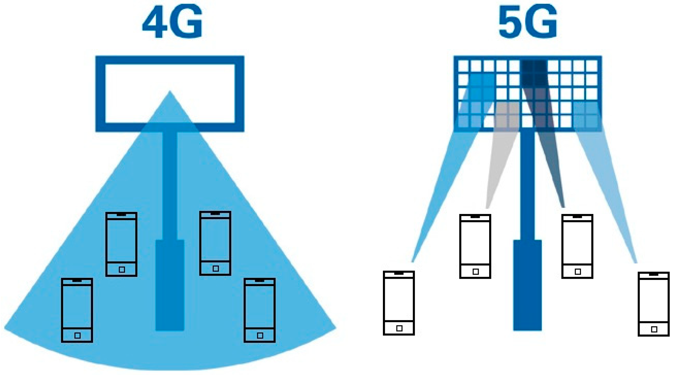
:1. Introduction
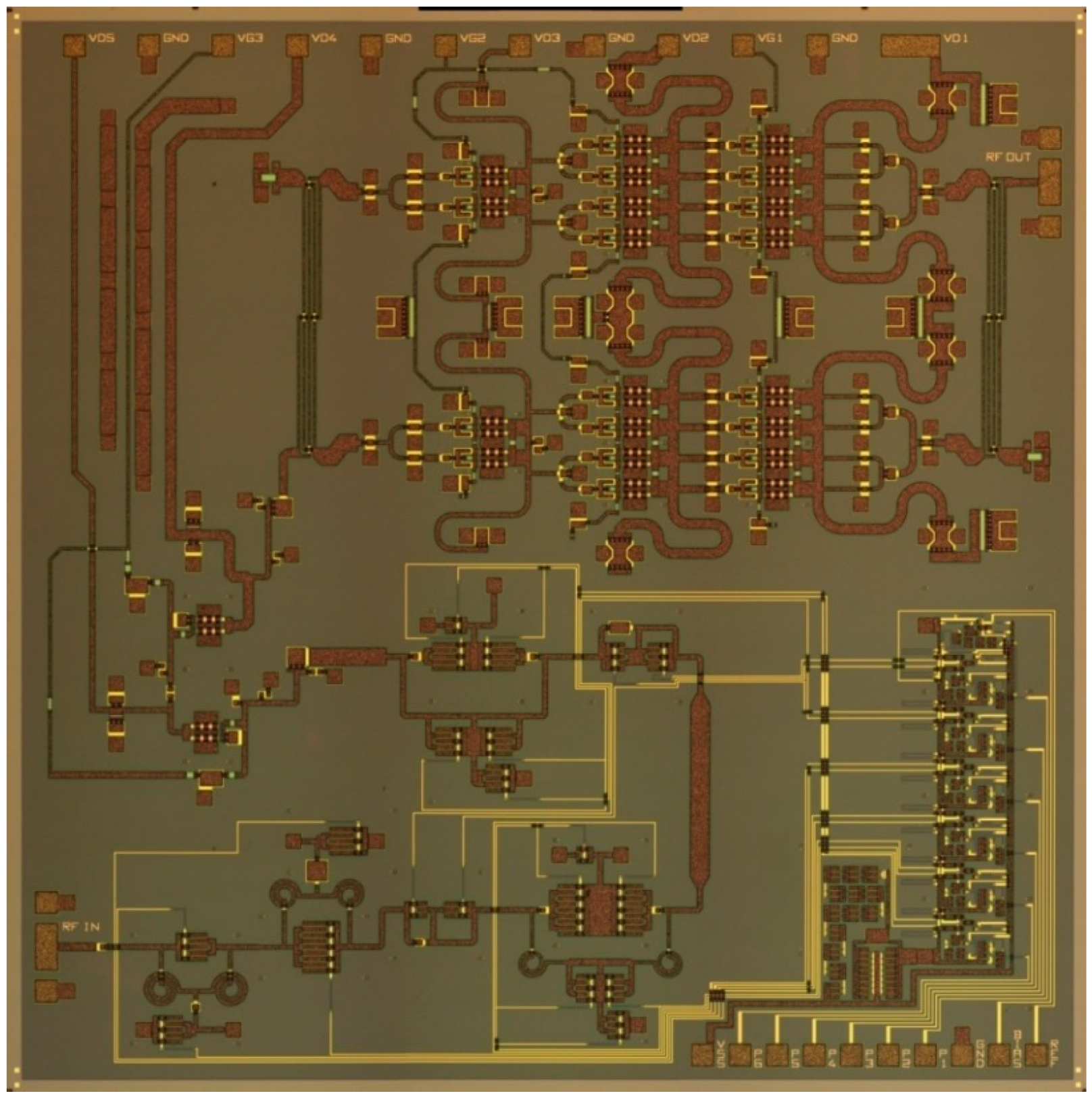
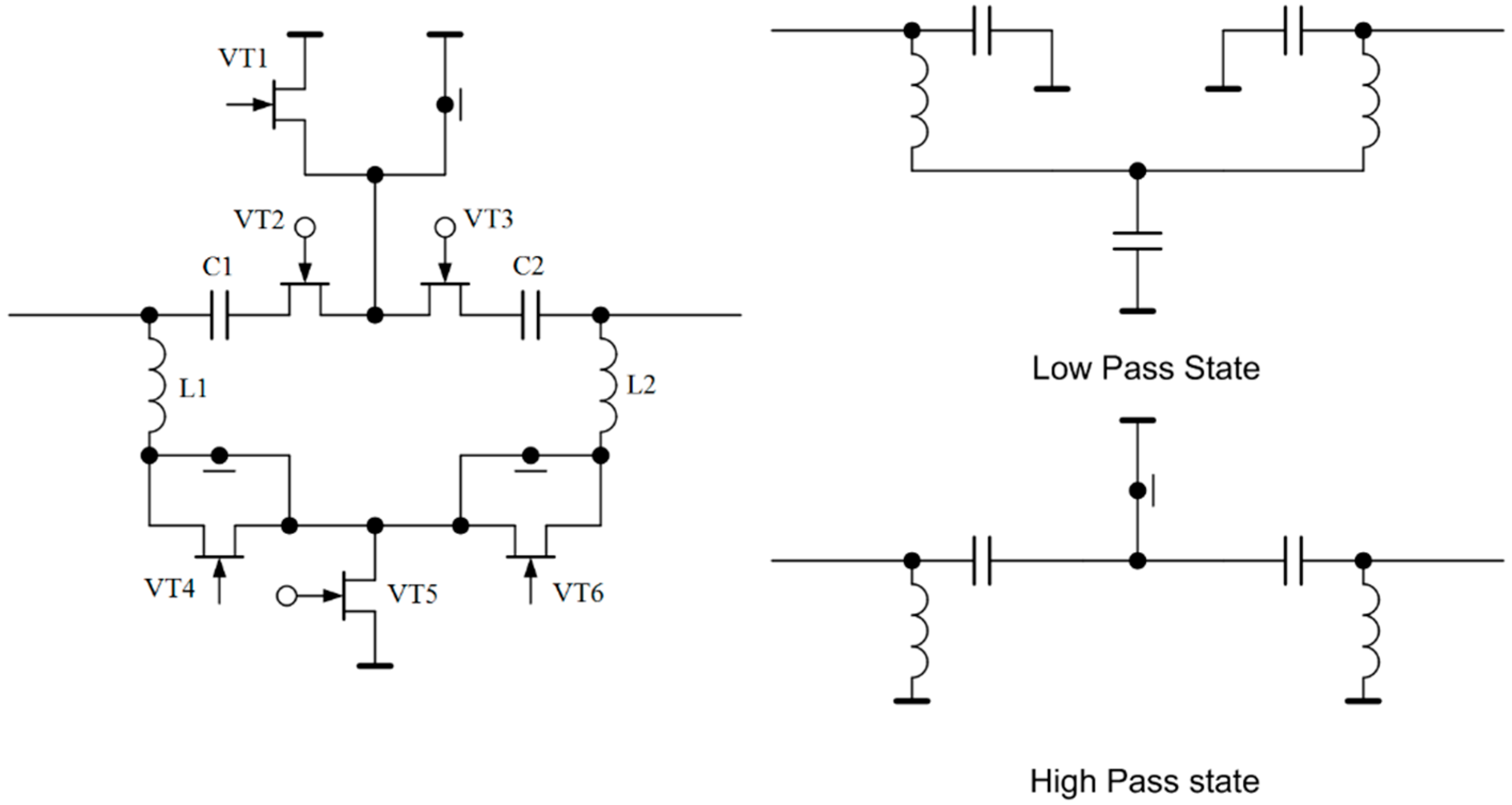
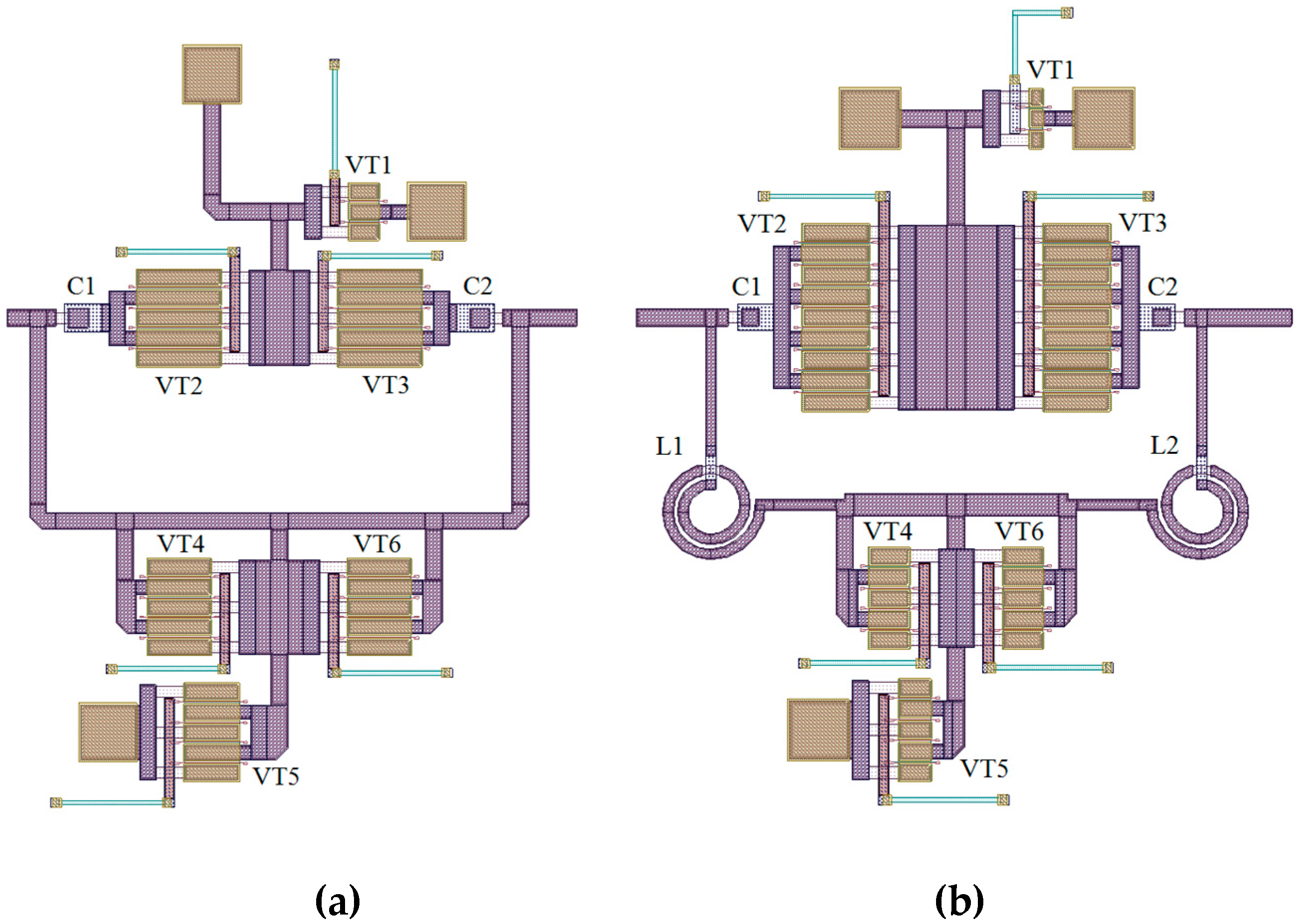
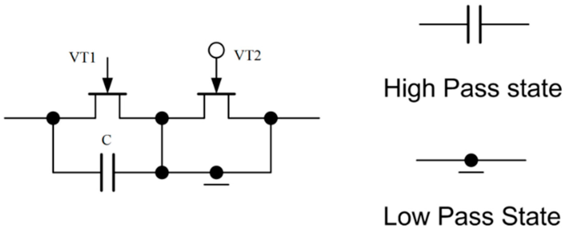
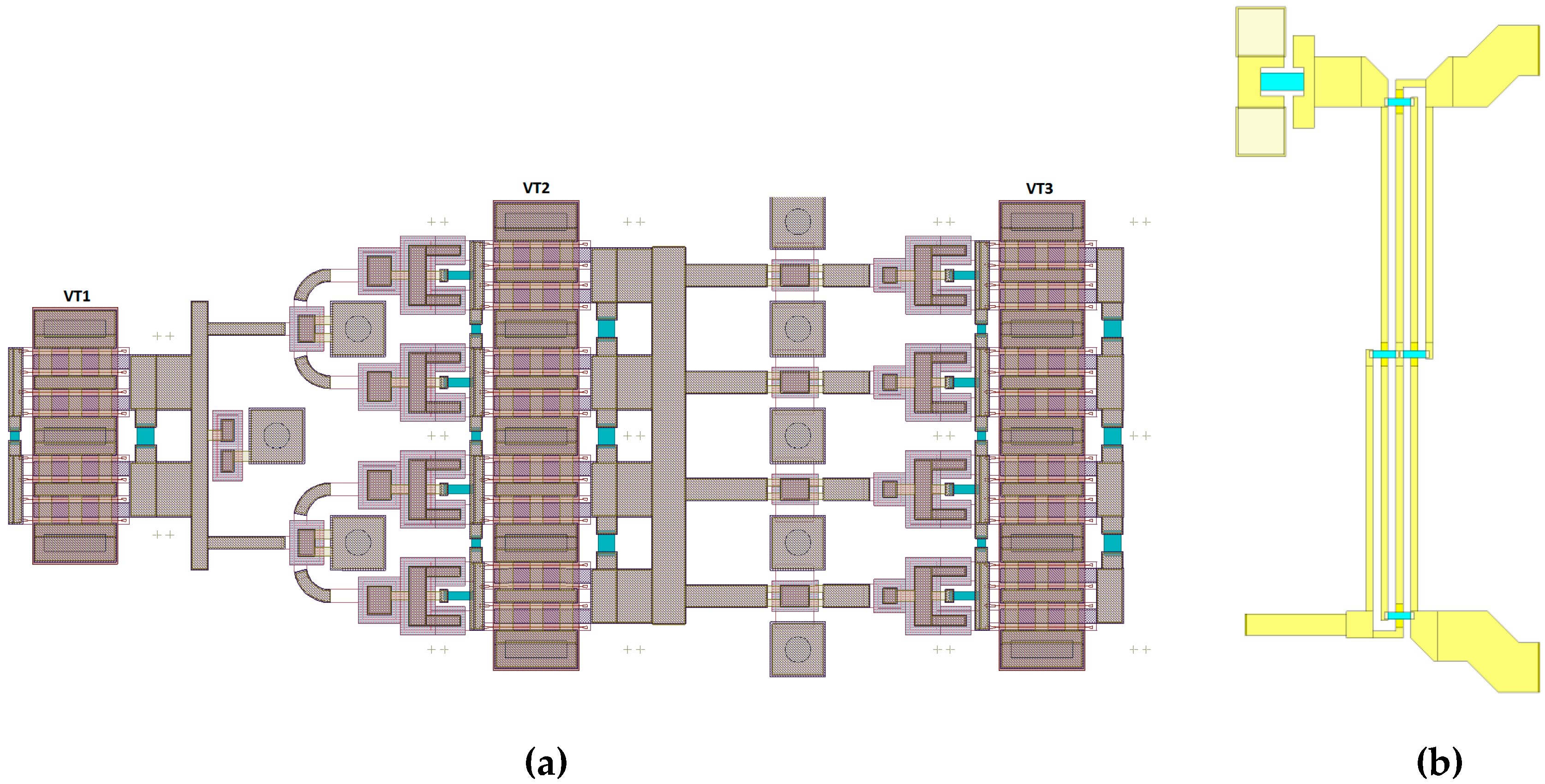
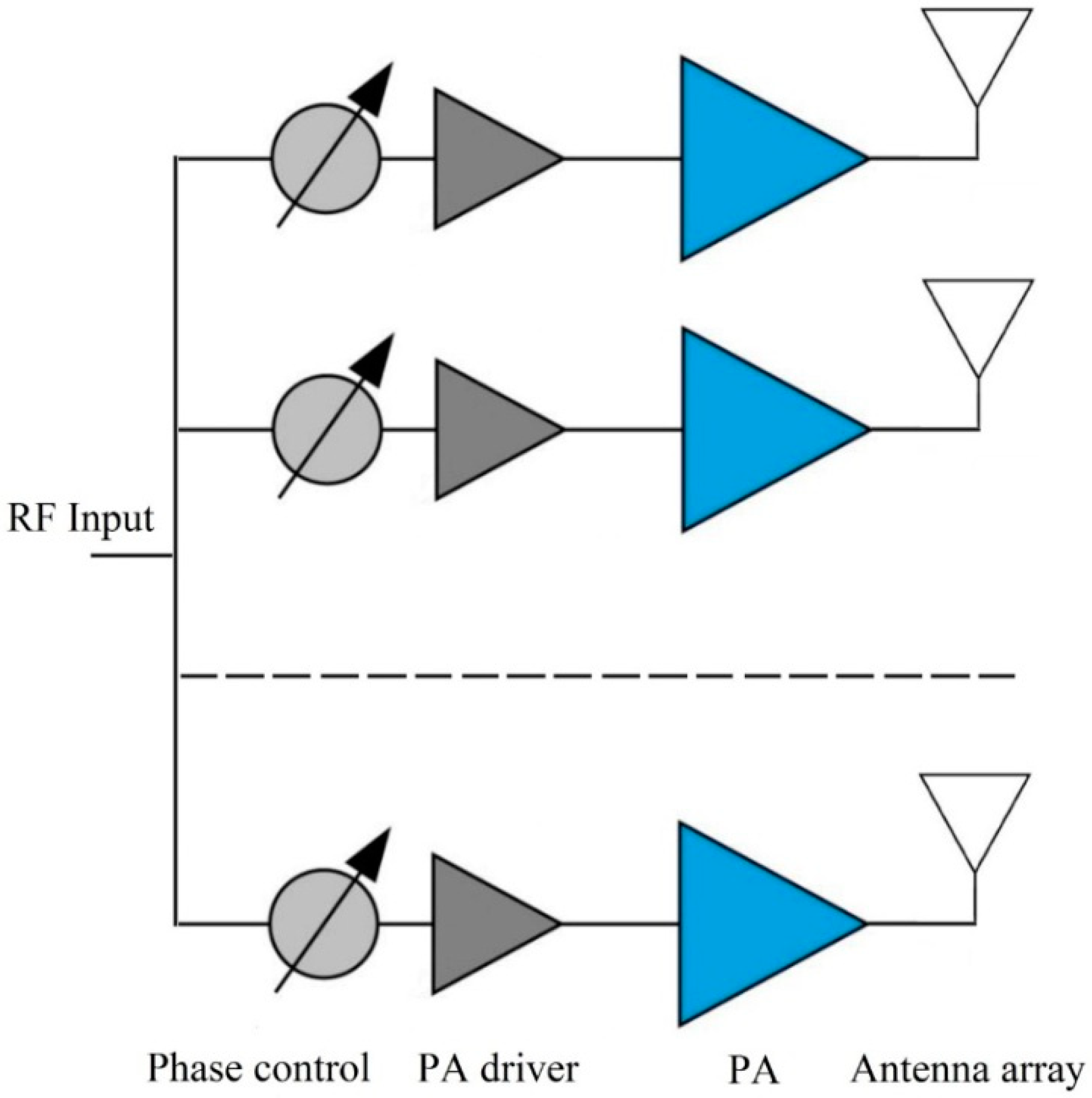
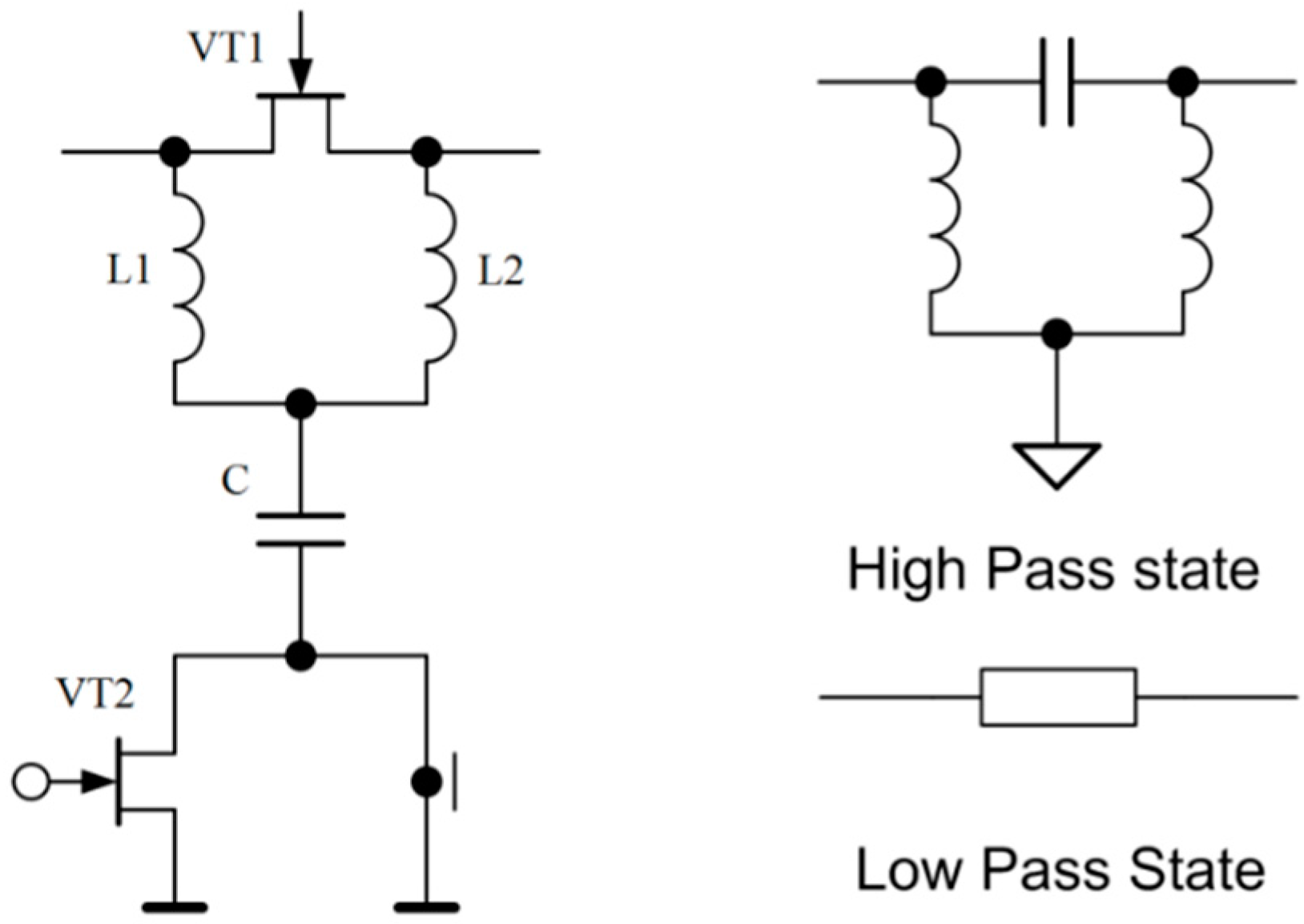
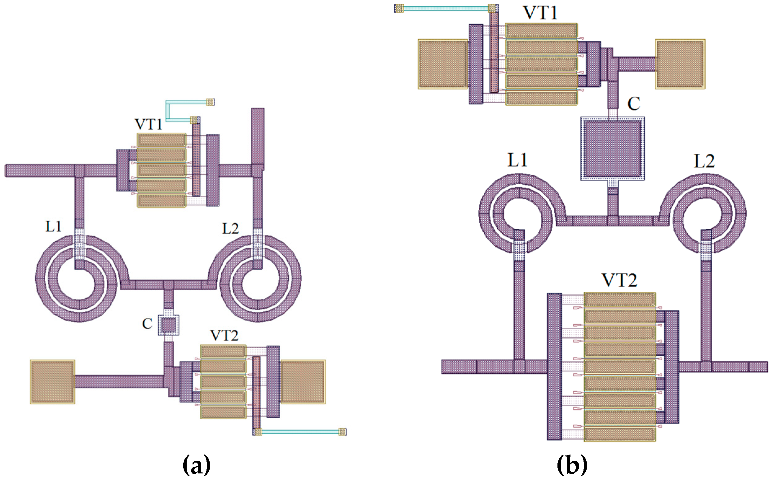
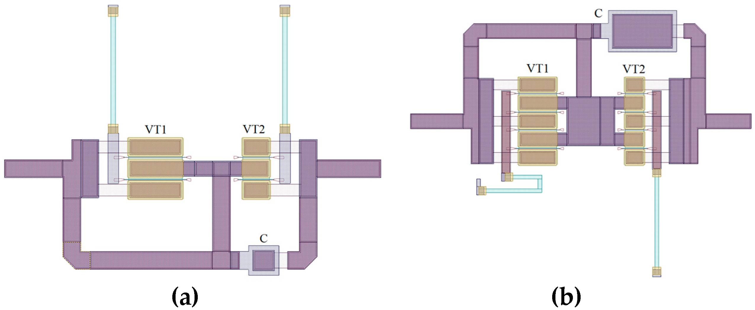
2. Single-Chip RF Front-End MMIC
2.1. Design Approach
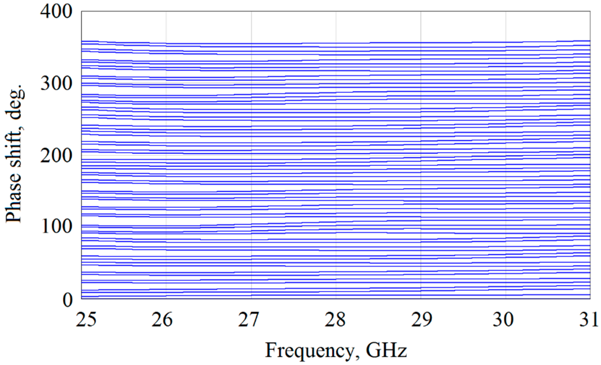
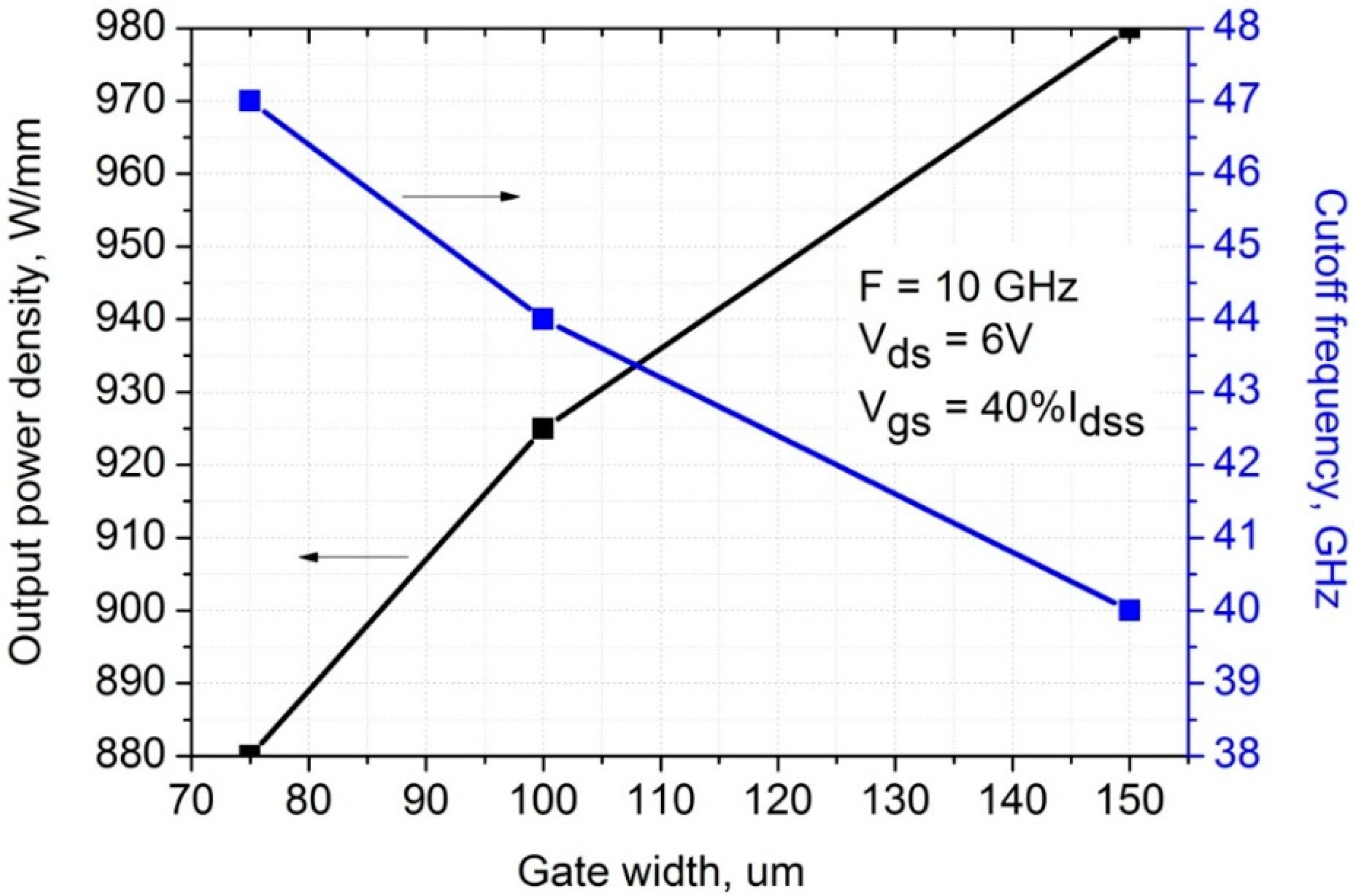
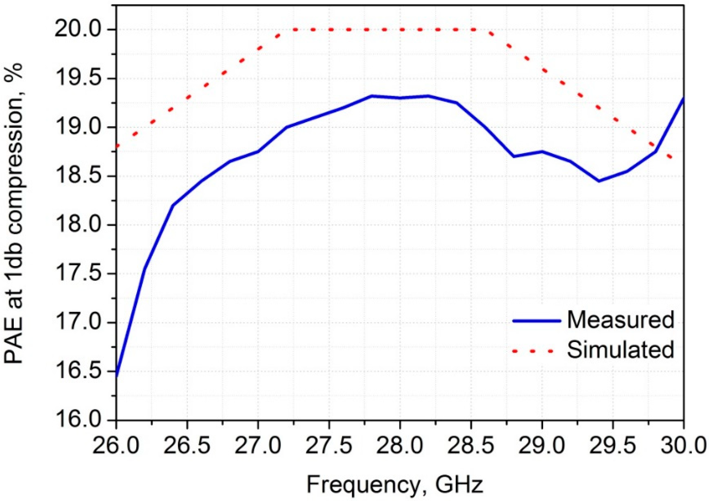
2.2. Electrical Performance
3. Conclusions
Author Contributions
Funding
Conflicts of Interest
Appendix A

| Bit1 | Bit2 | Bit3 | Bit4 | Bit5 | Bit6 | Relative Phase Shift, deg. |
|---|---|---|---|---|---|---|
| 0 | 0 | 0 | 0 | 0 | 0 | 0.000 |
| 1 | 0 | 0 | 0 | 0 | 0 | 5.625 |
| 0 | 1 | 0 | 0 | 0 | 0 | 11.250 |
| 1 | 1 | 0 | 0 | 0 | 0 | 16.875 |
| 0 | 0 | 1 | 0 | 0 | 0 | 22.500 |
| 1 | 0 | 1 | 0 | 0 | 0 | 28.125 |
| 0 | 1 | 1 | 0 | 0 | 0 | 33.750 |
| 1 | 1 | 1 | 0 | 0 | 0 | 39.375 |
| 0 | 0 | 0 | 1 | 0 | 0 | 45.000 |
| 1 | 0 | 0 | 1 | 0 | 0 | 50.625 |
| 0 | 1 | 0 | 1 | 0 | 0 | 56.250 |
| 1 | 1 | 0 | 1 | 0 | 0 | 61.875 |
| 0 | 0 | 1 | 1 | 0 | 0 | 67.500 |
| 1 | 0 | 1 | 1 | 0 | 0 | 73.125 |
| 0 | 1 | 1 | 1 | 0 | 0 | 78.750 |
| 1 | 1 | 1 | 1 | 0 | 0 | 84.375 |
| 0 | 0 | 0 | 0 | 1 | 0 | 90.000 |
| 1 | 0 | 0 | 0 | 1 | 0 | 95.625 |
| 0 | 1 | 0 | 0 | 1 | 0 | 101.250 |
| 1 | 1 | 0 | 0 | 1 | 0 | 106.875 |
| 0 | 0 | 1 | 0 | 1 | 0 | 112.500 |
| 1 | 0 | 1 | 0 | 1 | 0 | 118.125 |
| 0 | 1 | 1 | 0 | 1 | 0 | 123.750 |
| 1 | 1 | 1 | 0 | 1 | 0 | 129.375 |
| 0 | 0 | 0 | 1 | 1 | 0 | 135.000 |
| 1 | 0 | 0 | 1 | 1 | 0 | 140.625 |
| 0 | 1 | 0 | 1 | 1 | 0 | 146.250 |
| 1 | 1 | 0 | 1 | 1 | 0 | 151.875 |
| 0 | 0 | 1 | 1 | 1 | 0 | 157.500 |
| 1 | 0 | 1 | 1 | 1 | 0 | 163.125 |
| 0 | 1 | 1 | 1 | 1 | 0 | 168.750 |
| 1 | 1 | 1 | 1 | 1 | 0 | 174.375 |
| 0 | 0 | 0 | 0 | 0 | 1 | 180.000 |
| 1 | 0 | 0 | 0 | 0 | 1 | 185.625 |
| 0 | 1 | 0 | 0 | 0 | 1 | 191.250 |
| 1 | 1 | 0 | 0 | 0 | 1 | 196.875 |
| 0 | 0 | 1 | 0 | 0 | 1 | 202.500 |
| 1 | 0 | 1 | 0 | 0 | 1 | 208.125 |
| 0 | 1 | 1 | 0 | 0 | 1 | 213.750 |
| 1 | 1 | 1 | 0 | 0 | 1 | 219.375 |
| 0 | 0 | 0 | 1 | 0 | 1 | 225.000 |
| 1 | 0 | 0 | 1 | 0 | 1 | 230.625 |
| 0 | 1 | 0 | 1 | 0 | 1 | 236.250 |
| 1 | 1 | 0 | 1 | 0 | 1 | 241.875 |
| 0 | 0 | 1 | 1 | 0 | 1 | 247.500 |
| 1 | 0 | 1 | 1 | 0 | 1 | 253.125 |
| 0 | 1 | 1 | 1 | 0 | 1 | 258.750 |
| 1 | 1 | 1 | 1 | 0 | 1 | 264.375 |
| 0 | 0 | 0 | 0 | 1 | 1 | 270.000 |
| 1 | 0 | 0 | 0 | 1 | 1 | 275.625 |
| 0 | 1 | 0 | 0 | 1 | 1 | 281.250 |
| 1 | 1 | 0 | 0 | 1 | 1 | 286.875 |
| 0 | 0 | 1 | 0 | 1 | 1 | 292.500 |
| 1 | 0 | 1 | 0 | 1 | 1 | 298.125 |
| 0 | 1 | 1 | 0 | 1 | 1 | 303.750 |
| 1 | 1 | 1 | 0 | 1 | 1 | 309.375 |
| 0 | 0 | 0 | 1 | 1 | 1 | 315.000 |
| 1 | 0 | 0 | 1 | 1 | 1 | 320.625 |
| 0 | 1 | 0 | 1 | 1 | 1 | 326.250 |
| 1 | 1 | 0 | 1 | 1 | 1 | 331.875 |
| 0 | 0 | 1 | 1 | 1 | 1 | 337.500 |
| 1 | 0 | 1 | 1 | 1 | 1 | 343.125 |
| 0 | 1 | 1 | 1 | 1 | 1 | 348.750 |
| 1 | 1 | 1 | 1 | 1 | 1 | 354.375 |
References
- Osseiran, A. 5G Mobile and Wireless Communications Technology; Cambridge University Press: Cambridge, UK, 2016. [Google Scholar]
- Agiwal, L.; Roy, A.; Saxena, N. Next generation 5G wireless networks: A comprehensive survey. IEEE Commun. Surv. Tutor. 2016, 18, 1617–1655. [Google Scholar] [CrossRef]
- Marcus, M. 5G and “IMT for 2020 and beyond”. IEEE Wirel. Commun. Mag. 2015, 22, 2–3. [Google Scholar] [CrossRef]
- Albreem, M. 5G wireless communication systems: Vision and challenges. In Proceedings of the 2015 International Conference on Computer, Communications, and Control Technology (I4CT) 2015, Kuching, Malaysia, 21–23 April 2015; pp. 493–497. [Google Scholar]
- International Telecommunications Union. 2019. Available online: http://www.itu.int/en/ITU-R/study-groups/rsg5/rwp5d/imt-2020/Pages/default.aspx (accessed on 1 July 2020).
- Federal Communications Commission 2020: Upper Microwave Flexible Use Service Millimeter Frequency Bands. Available online: https://www.fcc.gov/wireless/bureau-divisions/broadband-division/upper-microwave-flexible-use-service-umfus (accessed on 1 July 2020).
- Testa, F.; Pavesi, L. Optical Switching in Next Generation Data Centers; Springer International Publishing: Cham, Switzerland, 2018. [Google Scholar]
- Liu, X. Emerging optical access network technologies for 5G wireless. IEEE/OSA J. Opt. Commun. Netw. 2016, 8, B70–B79. [Google Scholar] [CrossRef]
- Roh, W.; Seol, J.; Park, J.; Lee, B.; Lee, J.; Kim, Y.; Cho, J.; Cheun, K.; Aryanfar, F. Millimeter-wave beamforming as an enabling technology for 5G cellular communications: Theoretical feasibility and prototype results. IEEE Commun. Mag. 2014, 52, 106–113. [Google Scholar] [CrossRef]
- Gupta, A.; Jha, R. A survey of 5G network: Architecture and emerging technologies. IEEE Access. 2015, 3, 1206–1232. [Google Scholar] [CrossRef]
- Zhou, B.; Liu, A.; Lau, V. Successive localization and beamforming in 5G mmWave MIMO communication systems. IEEE Trans. Signal Process. 2019, 67, 1620–1635. [Google Scholar] [CrossRef]
- Yang, B.; Yu, Z.; Lan, J.; Zhang, R.; Zhou, J.; Hong, W. Digital Beamforming-Based Massive MIMO Transceiver for 5G Millimeter-Wave Communications. IEEE Trans. Microw. Theory Tech. 2018, 66, 1–16. [Google Scholar] [CrossRef]
- Vook, F.; Ghosh, A.; Thomas, T. MIMO and beamforming solutions for 5G technology. IEEE Int. Microw. Symp. 2014, 1–4. [Google Scholar] [CrossRef]
- Glynn, S.; Devlin, L. A 28GHz, 4-channel Phase Adjustable Power Amplifier IC for 5G front-ends. In Proceedings of the Automated RF & Microwave Measurement Society (ARMMS) Conference, Oxford Belfry, Nr Thame, UK, 20–21 April 2015. [Google Scholar]
- Devlin, L. The Design of Integrated Switches and Phase Shifters. In Proceedings of the IEEE Tutorial Colloquium on Design of RFICs and MMICs. 1999, pp. 1–14. Available online: https://ieeexplore.ieee.org/document/827279 (accessed on 1 June 2020).
- AWR Microwave Office Software. Available online: https://www.awr.com/awr-software/products/microwave-office (accessed on 6 July 2020).


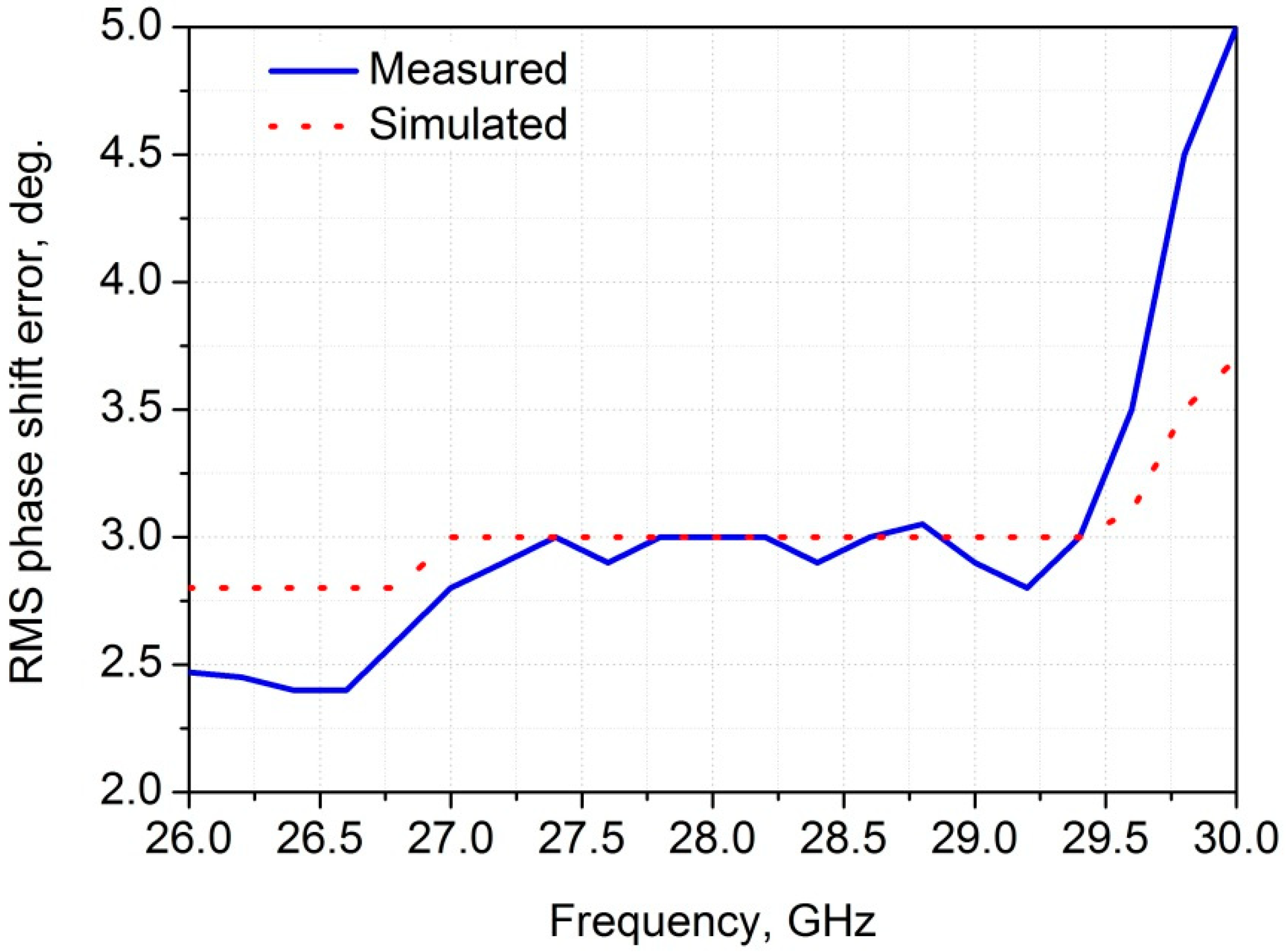
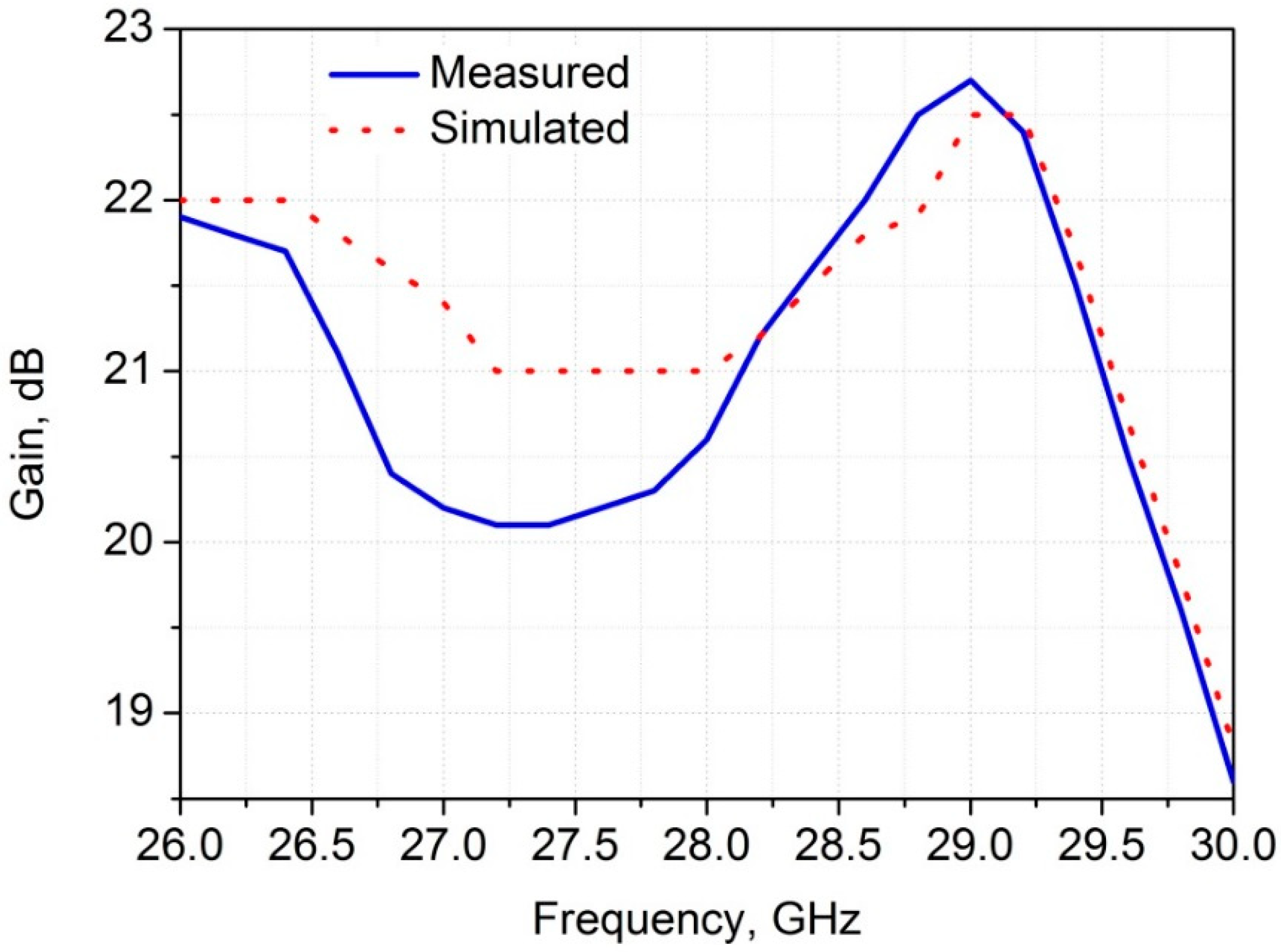
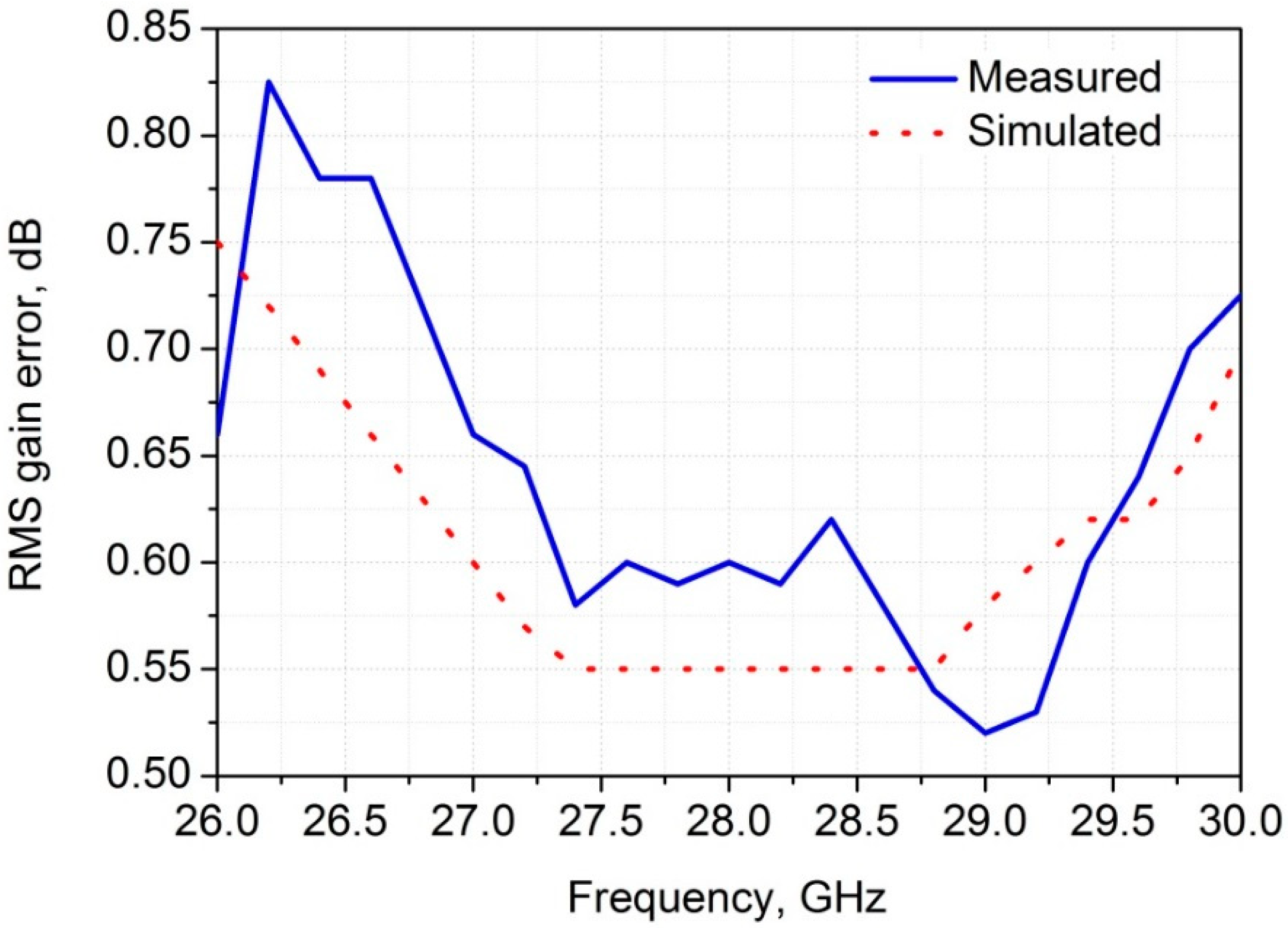
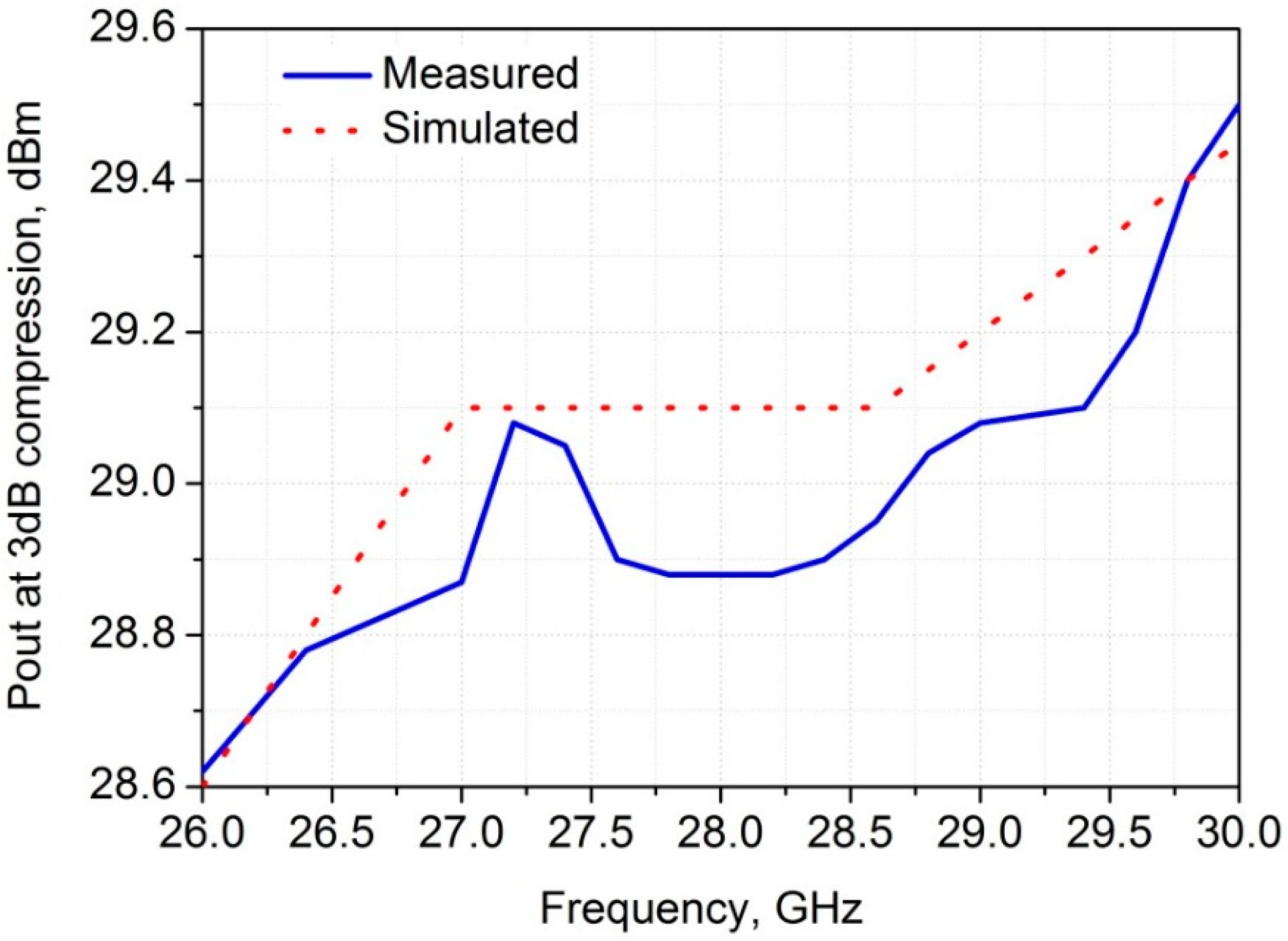
| This Work | Ref. [14] | ||||
|---|---|---|---|---|---|
| Parameter | Min | Max | Min | Max | Units |
| Frequency | 27.5 | 28.35 | 27.5 | 28.35 | GHz |
| RMS Phase Error | 3 | 2.38 | deg. | ||
| RMS Gain Error | 0.63 | 0.23 | dB | ||
| Gain | 20.0 | 21.3 | 20.5 | 21.5 | dB |
| P1dB at 0° | - | - | 29.8 | 30.2 | dBm |
| P3dB at 0° | 28.7 | 29.0 | - | - | dBm |
| PAE at P1dB at 0° | 19.2 | 19.3 | 23 | 24.2 | % |
© 2020 by the authors. Licensee MDPI, Basel, Switzerland. This article is an open access article distributed under the terms and conditions of the Creative Commons Attribution (CC BY) license (http://creativecommons.org/licenses/by/4.0/).
Share and Cite
Erofeev, E.; Arykov, V.; Stepanenko, M.; Voevodin, A.; Kogai, A.; Kurikalov, V. 28 GHz Single-Chip Transmit RF Front-End MMIC for Multichannel 5G Wireless Communications. Symmetry 2020, 12, 1167. https://doi.org/10.3390/sym12071167
Erofeev E, Arykov V, Stepanenko M, Voevodin A, Kogai A, Kurikalov V. 28 GHz Single-Chip Transmit RF Front-End MMIC for Multichannel 5G Wireless Communications. Symmetry. 2020; 12(7):1167. https://doi.org/10.3390/sym12071167
Chicago/Turabian StyleErofeev, Evgeny, Vadim Arykov, Michael Stepanenko, Aleksei Voevodin, Aleksei Kogai, and Vladimir Kurikalov. 2020. "28 GHz Single-Chip Transmit RF Front-End MMIC for Multichannel 5G Wireless Communications" Symmetry 12, no. 7: 1167. https://doi.org/10.3390/sym12071167
APA StyleErofeev, E., Arykov, V., Stepanenko, M., Voevodin, A., Kogai, A., & Kurikalov, V. (2020). 28 GHz Single-Chip Transmit RF Front-End MMIC for Multichannel 5G Wireless Communications. Symmetry, 12(7), 1167. https://doi.org/10.3390/sym12071167