1. Introduction
Advancement in battery technology has not kept pace with the advancement of semiconductor technology, and hence the energy efficiency of electronic circuits and systems deployed in portable and mobile applications is an important concern. To achieve improvement in the energy efficiency, approximate computing is considered to be an attractive alternative to conventional accurate computing [
1]. Approximate computing has the potential to enable simultaneous reductions in all the design metrics such as delay, area, and power/energy [
2], while providing an acceptable compromise in the accuracy of results. The case for approximate computing is pertinent, because practical multimedia applications [
3] involving digital signal processing, such as digital image or video or audio processing are naturally resilient to inaccuracies, because a minor distortion in an image or a video frame or a feeble noise in an audio are not practically discernible by humans.
Approximate computing covers hardware [
4], software [
5], and memories [
6], and with respect to hardware, approximate computing includes approximate arithmetic circuits [
7] and approximate logic circuits [
8]. With respect to approximate arithmetic circuits, the primary focus has been on the design of approximate adders and multipliers. This is because addition and multiplication form the basis of computer arithmetic, and they are fundamental operations which are frequently encountered in practically all electronics and communication systems.
Thus far, many approximate adders have been presented in the literature, and they primarily correspond to the synchronous design method [
7]. Among them, some of the approximate adders are ASIC based involving either a full-custom transistor level implementation or a semi-custom gate level implementation, while a few approximate adders [
9,
10] correspond to a pure FPGA based design. However, some approximate adders are suitable for both ASIC and FPGA implementations, which include LOA [
11], LOAWA [
12], APPROX5 [
13], HEAA [
14], OLOCA [
15] and HOERAA [
16], as noted in [
16]. A brief preliminary work [
17] discussed the asynchronous quasi-delay-insensitive (QDI) implementation of just the LOA architecture, by assuming arbitrary sizes of accurate and inaccurate adder parts. However, the error parameters corresponding to the LOA architecture were not provided, and no practical application was considered to demonstrate the usefulness of approximate addition. In contrast, this article makes the following contributions:
Asynchronous QDI implementation of approximate addition based on different approximate adder architectures, such as LOA, LOAWA, APPROX5, HEAA, OLOCA and HOERAA is described alongside the accurate addition.
Design metrics of the accurate QDI adder and different approximate QDI adders are estimated and compared by considering a delay-insensitive dual-rail data encoding and return-to-zero (RTZ) and return-to-one (RTO) handshaking. The implementations use a 32/28-nm complementary metal oxide semiconductor (CMOS) process technology.
Popular error metrics widely used in approximate computing are calculated for the approximate adders and provided for a comparison. The error distribution of the approximate adders is also portrayed. The implementation of the adders and their error metrics correspond to a digital image processing application.
A digital image processing application is considered to demonstrate the practical usefulness of approximate addition vis-à-vis the accurate addition.
The above contributions would be useful, because this work attempts to showcase in detail the twin advantages of approximate computing and an asynchronous QDI implementation. While approximate arithmetic could lead to an enhanced energy efficiency compared to accurate arithmetic, an asynchronous QDI implementation is bestowed with many advantages, such as natural resilience to electromagnetic interference [
18], innate tolerance to process, temperature, supply and threshold voltage variations [
19], inherent resistance to power analysis attacks [
20], and self-checking ability [
21], all of which bodes well for modern electronic designs.
The rest of the article is organized as follows.
Section 2 discusses the fundamentals of QDI circuit design.
Section 3 describes the QDI implementation of accurate and approximate adders based on RTZ and RTO handshaking.
Section 4 presents the implementation results. The error metrics of the approximate adders are given in
Section 5, and the digital image processing results corresponding to accurate and approximate additions are given in
Section 6.
Section 7 concludes the article.
2. QDI Circuit Design—Fundamentals
QDI circuits are the practically realizable delay-insensitive (DI) circuits. QDI circuits incorporate the isochronicity assumption [
22], which is implicit in an isochronic fork. An isochronic fork implies that when two or more wires branch out from an electrical node, any signal transition on the node is assumed to appear concurrently on all the wires forking out from that node. However, not all of the nodes in a QDI circuit have to be isochronic, but the isochronic fork assumption is generally imposed on all the primary inputs associated with a QDI circuit stage. This is because the primary inputs are given to a QDI circuit and also to a completion detector. Hence, the primary inputs are meant to reach a QDI circuit, as well as the completion detector simultaneously through isochronic nodes. In general, the isochronic fork assumption is restricted to small circuit areas and they are shown to be realizable even in nanoscale design geometries [
23]. Therefore, QDI circuits are also realizable in nanoscale design geometries.
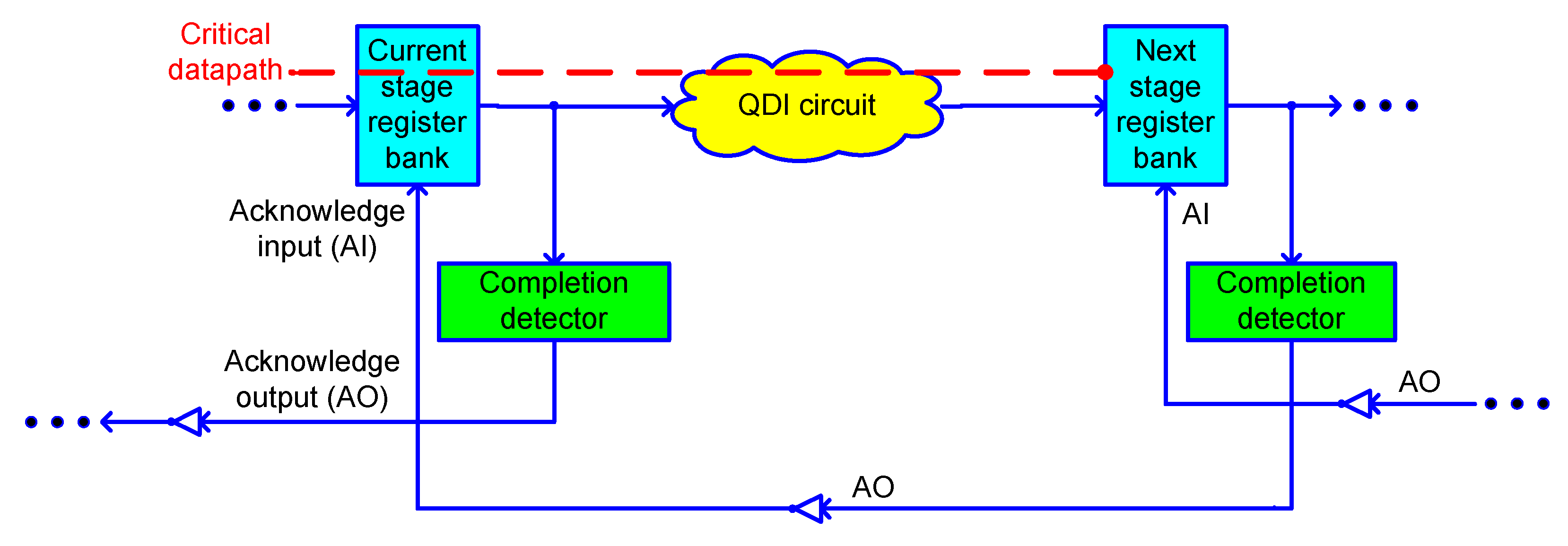
The block schematic of a QDI asynchronous circuit stage is shown in
Figure 1. A QDI circuit stage comprises a current stage register bank that receives the inputs, a completion detector that indicates, i.e., acknowledges the receipt of all the inputs, and a QDI circuit that does the processing. Inputs are supplied from the current stage register bank to the QDI circuit, as well as to the completion detector. The next stage register bank, which receives the outputs, would serve as the current stage register bank for the successive QDI circuit stage. Acknowledge input (AI) and acknowledge output (AO) are the handshake signals that are exchanged between the current and next stage register banks. AI is the Boolean complement of AO and vice versa.
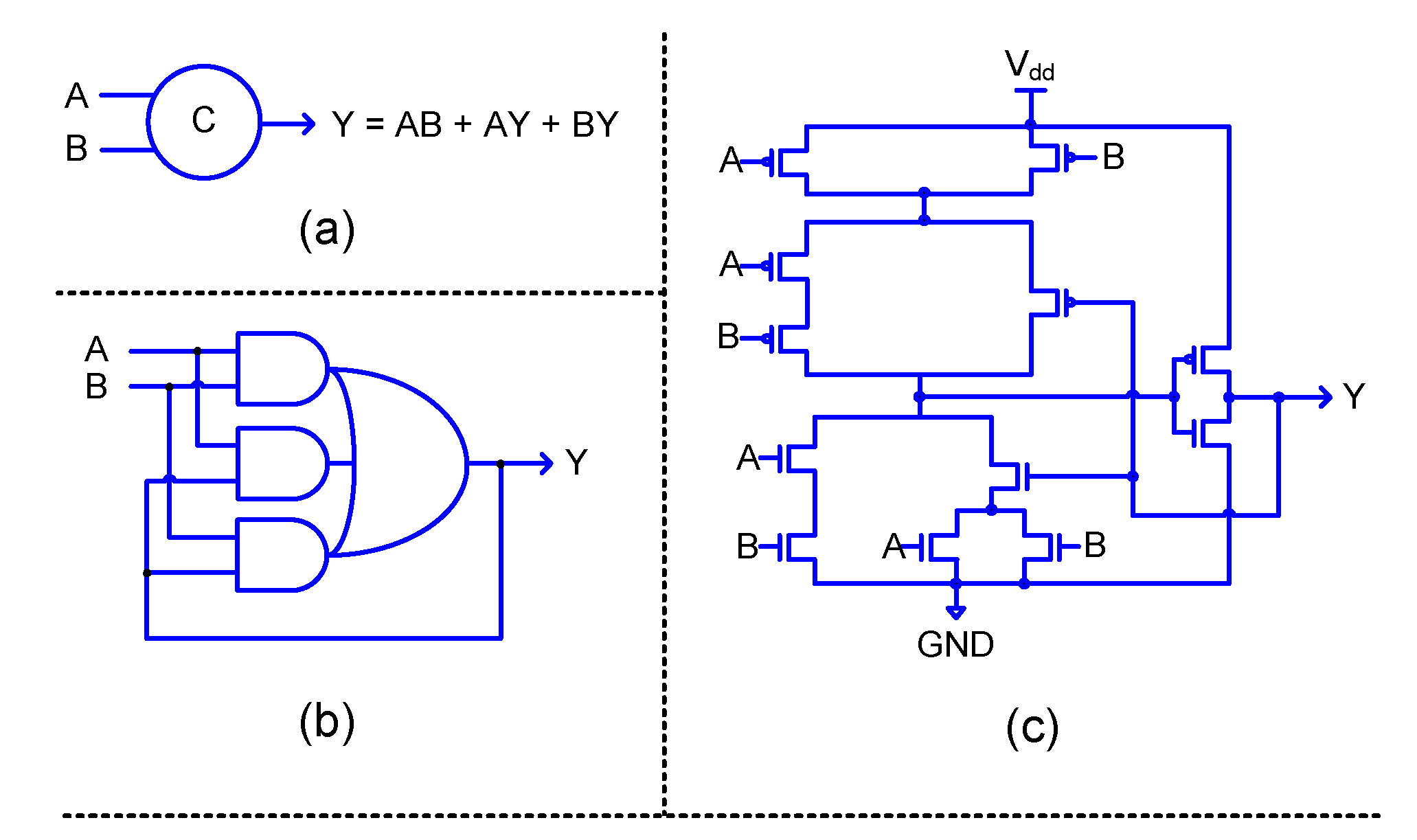
In a synchronous circuit, a register bank would comprise flip-flops. In a QDI circuit, a current or next stage register bank would consist of 2-input C-elements. The C-element [
24] will output binary 1 if all its inputs are one and output binary 0 if all its inputs are zero. The C-element will maintain its existing steady state if its inputs are not the same. The logic symbol, and gate level and transistor level realizations of a 2-input C-element are shown in
Figure 2, where A and B denote the inputs and Y denotes the output. Incorporating feedback in an AO222 complex gate would help to realize a 2-input C-element.
2.1. Delay-Insensitive Data Encoding and Four-Phase Handshaking
QDI circuits generally adopt an
m-of-
n encoding scheme for data representation and a four-phase handshake protocol for data communication. The dual-rail or 1-of-2 code is the simplest and widely used
m-of-
n code [
25]. With reference to
Figure 1, all the inputs given to a QDI circuit and all the outputs produced by it are assumed to be dual-rail encoded here. Dual-rail encoding of data is performed according to the handshake protocol used. There are two four-phase handshake protocols available namely return-to-zero (RTZ) [
26] and return-to-one (RTO) [
27].
Based on RTZ handshaking, an input I is encoded into two wires as say I1 and I0, where I = 1 is encoded as I1 = 1 and I0 = 0, and I = 0 is encoded as I0 = 1 and I1 = 0. These two assignments are called data. I1 = I0 = 0 is called the spacer, and I1 = I0 = 1 is considered to be indeterminate or invalid.
Both RTZ and RTO handshake protocols involve four phases to complete a data transaction. According to RTZ handshaking, in the first phase, the dual-rail data bus initially assumes the spacer and hence AI = 1. After the current stage register bank sends data, rising signal transitions, i.e., 0 to 1 would occur on one of the rails of each dual-rail encoded input of the data bus. In the second phase, the next stage register bank, after receiving the processed data from the QDI circuit, would drive AO to 1. In the third phase, the current stage register bank would wait for AI to become 0, and after this happens, the data bus would once again assume the spacer. In the fourth phase, after a finite and positive but unbounded time, the next stage register bank would receive the spacer from the QDI circuit and would drive AO to 0. Eventually, AI will assume 1. With this, one data transaction is said to be completed. In RTZ handshaking, the application of data is followed by the application of the spacer, and so on.
Based on RTO handshaking, an input I is encoded into two wires as say I1 and I0, where I = 1 is encoded as I1 = 0 and I0 = 1, and I = 0 is encoded as I0 = 0 and I1 = 1. These two assignments are called data. I1 = I0 = 1 is called the spacer, and I1 = I0 = 0 is considered to be indeterminate or invalid.
According to RTO handshaking, in the first phase, initially AI = 1. The current stage register bank first sends the spacer, and, as a result, rising signal transitions will occur on all the rails of the data bus. In the second phase, the next stage register bank, after receiving the spacer from the QDI circuit would drive AO to 1. In the third phase, the current stage register bank would wait for AI to assume 0, and, after this happens, the data bus would send the data by permitting falling signal transitions, i.e., 1 to 0 to occur on one of the rails of each dual-rail encoded input of the data bus. In the fourth phase, after a finite and positive (but unbounded) time, the next stage register bank would receive the processed data from the QDI circuit and subsequently drive AO to 0. Eventually, AI will assume 1, and with this, one data transaction is said to be completed. In RTO handshaking, the application of the spacer is followed by the application of data, and so on.
Regardless of whether the handshake protocol used is RTZ or RTO, the spacer separates two input data. The cycle time, which is given by the sum of the critical path delays encountered in processing a data (i.e., forward latency) and the spacer (i.e., reverse latency), governs the speed of a QDI circuit. The critical data path is highlighted in
Figure 1. The cycle time corresponds to the time taken for one data transaction, and it determines the operating speed of a QDI circuit.
2.2. Kinds of QDI Circuits
There are three kinds of QDI circuits namely strong-indication and weak-indication [
28], and early output [
29]. Strong-indication circuits require all the inputs to process and produce all the outputs. Weak-indication circuits may process and produce all but one of the outputs after receiving all but one of the inputs. However, only after receiving the last input, they can process and produce the last output. Early output circuits can process and produce all the outputs after receiving a subset of the inputs. Nevertheless, the completion detector associated with a QDI circuit, as shown in
Figure 1, would acknowledge the late arriving inputs. The early output nature is manifested in an early output circuit for the application of data or the spacer or sometimes for both.
3. QDI Implementation of Accurate and Approximate Adders
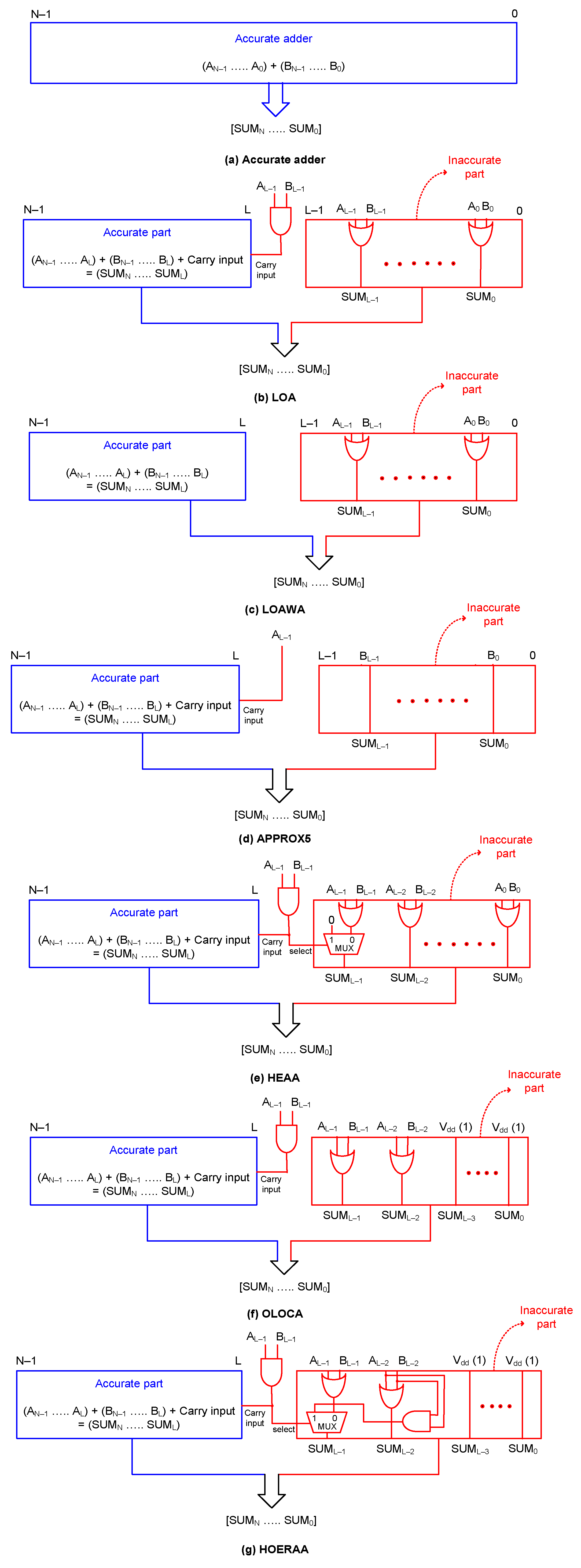
Generic (single-rail) block schematics of the accurate adder and the approximate adders LOA, LOAWA, APPROX5, HEAA, OLOCA and HOERAA are shown in
Figure 3, where N represents the adder width. The approximate adders consist of an inaccurate part, which is of size L bits, and an accurate part, which is of size (N–L) bits. The inaccurate part is less significant, while the accurate part is more significant. The accurate and inaccurate parts of the approximate adders are highlighted in blue and red, respectively, in
Figure 3.
In
Figure 3, A and B represent the adder inputs and SUM represents the adder output. The subscript 0 denotes the least significant bit of the adder inputs and output, subscript (N–1) denotes the most significant bit of the adder inputs, and subscript N denotes the most significant sum bit.
For the QDI implementation of accurate and approximate adders, whose schematics are shown in
Figure 3, we encoded all the adder inputs and outputs using dual-rail encoding corresponding to RTZ and RTO handshaking separately, as discussed in
Section 2. We uniformly considered the adder size as 32-bits. We allotted 10 bits to the inaccurate part and 22 bits to the accurate part of the approximate adders. This is because, for the digital image processing application that would be discussed in
Section 6, we found that an allocation of 10-bits to the inaccurate part yielded visually acceptable results for HOERAA, meaning that an image reproduced using approximate addition with a 10-bit inaccurate part was rather similar to the image reproduced via accurate addition.
Increasing the size of the inaccurate part beyond 10 bits affected the quality of the image reproduced with HOERAA-based approximate addition, so we restricted the size of the inaccurate part of approximate adders to 10 bits. Decreasing the size of the inaccurate part below 10 bits would help to improve the quality of the image reproduced with approximate addition; however, this would also reduce the savings in design metrics achievable compared to accurate addition. Hence, an optimum input partition should be chosen to strike an acceptable compromise between the quality of images reproduced and the potential reductions in design metrics achievable with approximate addition compared to accurate addition. Given this, we uniformly considered a 22-10 input partition for the approximate adders corresponding to the image processing application. Digital image processing shall be discussed in
Section 6, and, in this section, we discuss the QDI implementation of accurate and approximate adders.
While implementing a QDI circuit, the logic decomposition and optimization have to be performed safely [
30,
31] to maintain the quasi-delay-insensitivity. Otherwise, gate and wire orphans [
32] may result, which could affect the quasi-delay-insensitivity. In a QDI asynchronous circuit, an unacknowledged signal transition on an intermediate gate output is called as gate orphan and an unacknowledged signal transition on a wire is called a wire orphan. Wire orphans are usually overcome through the isochronic fork assumption. However, gate orphans may become problematic and to overcome them additional timing assumptions may have to be incorporated which might affect the quasi-delay-insensitivity. Hence, a safe logic decomposition and optimization is necessary to avoid gate orphans. Gate and wire orphans have been explained through circuit examples in [
33]—an interested reader may refer to the same for the details.
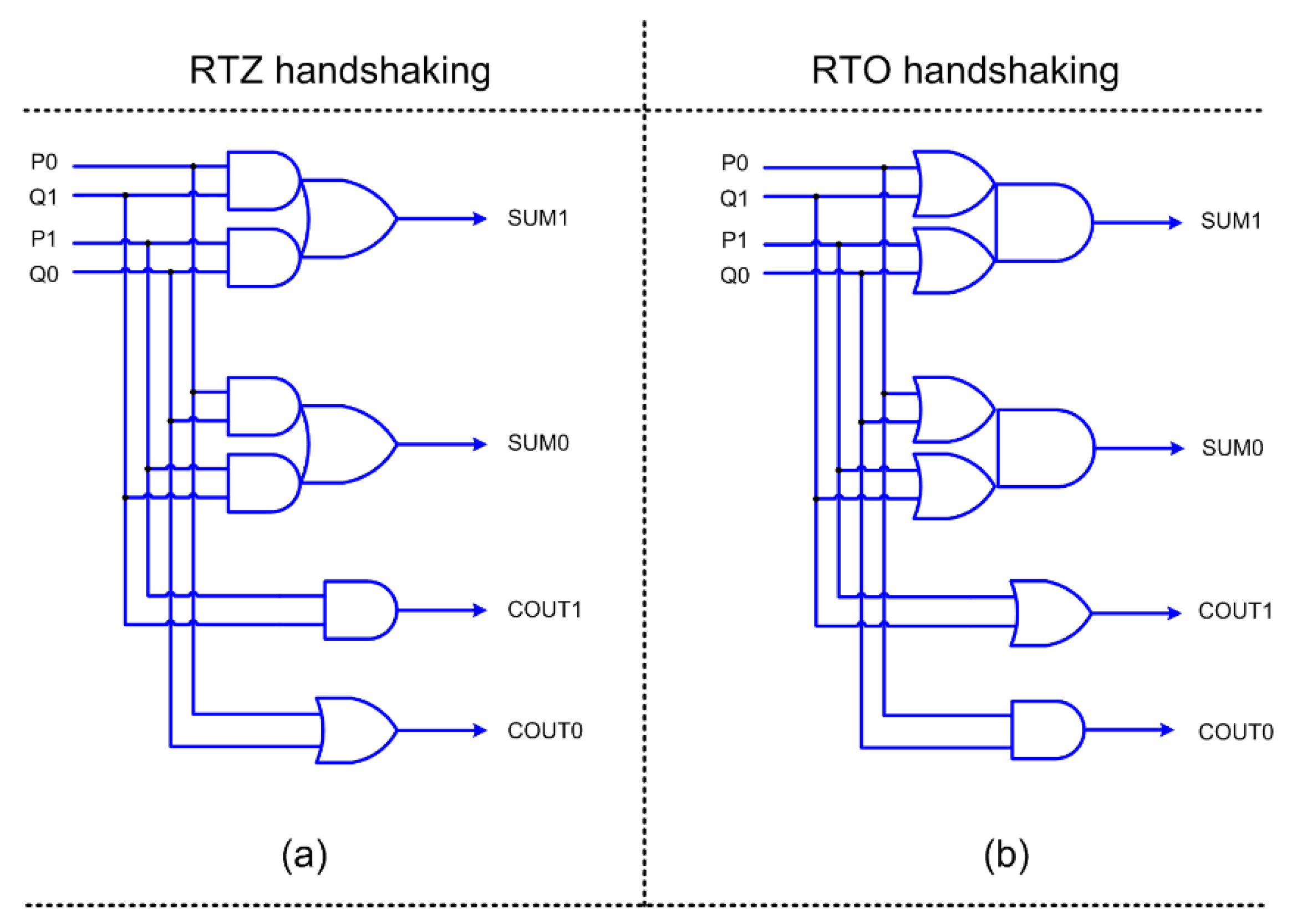
We used the early output half adder of [
34] and the early output full adder of [
35] to realize the accurate adder and accurate parts of the approximate adders shown in
Figure 3. Early output half adder corresponding to RTZ and RTO handshaking are shown in
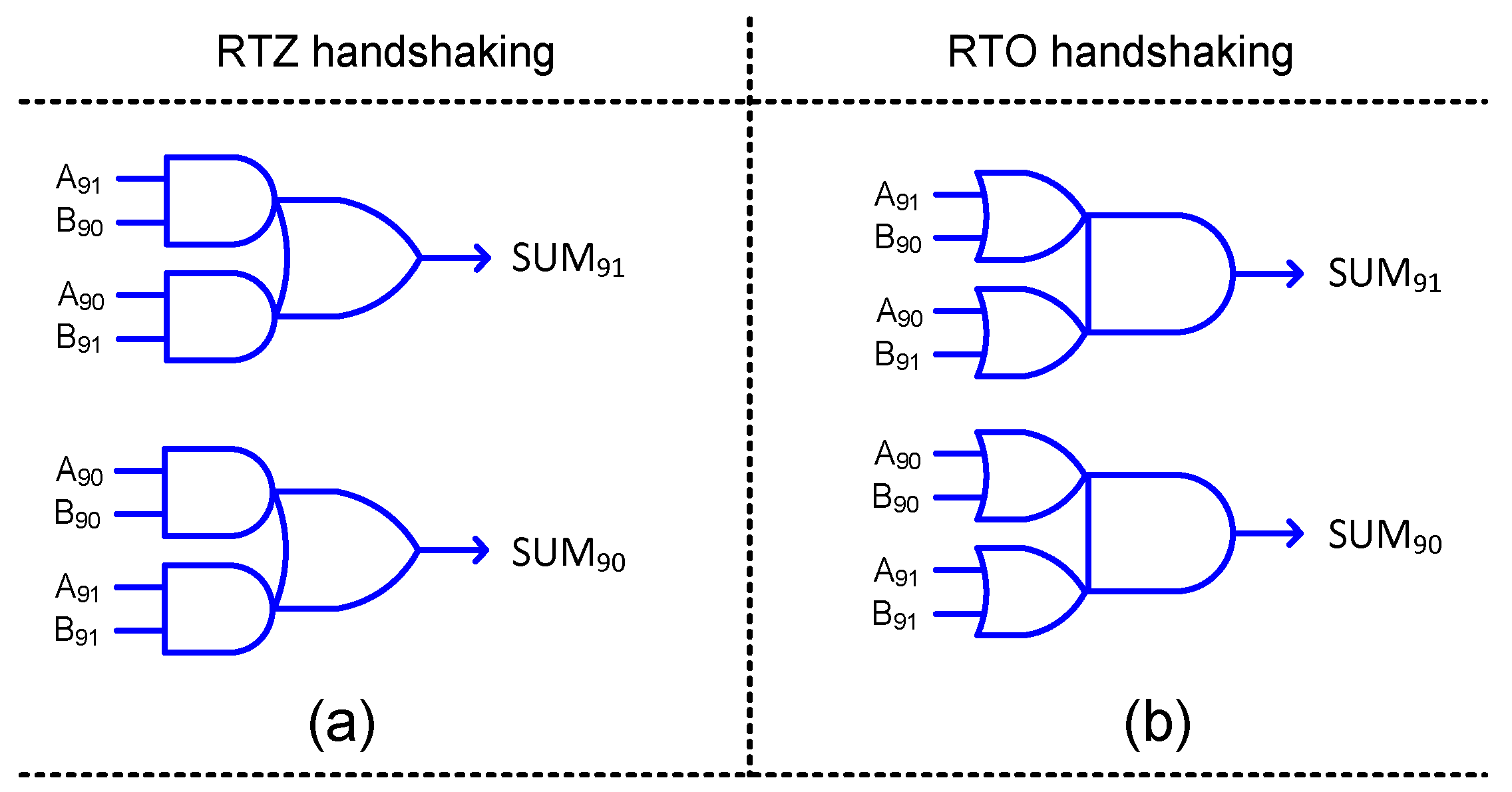
Figure 4a,b respectively, where (P1, P0) and (Q1, Q0) represent its dual-rail inputs, and (SUM1, SUM0) and (COUT1, COUT0) represent its dual-rail outputs.
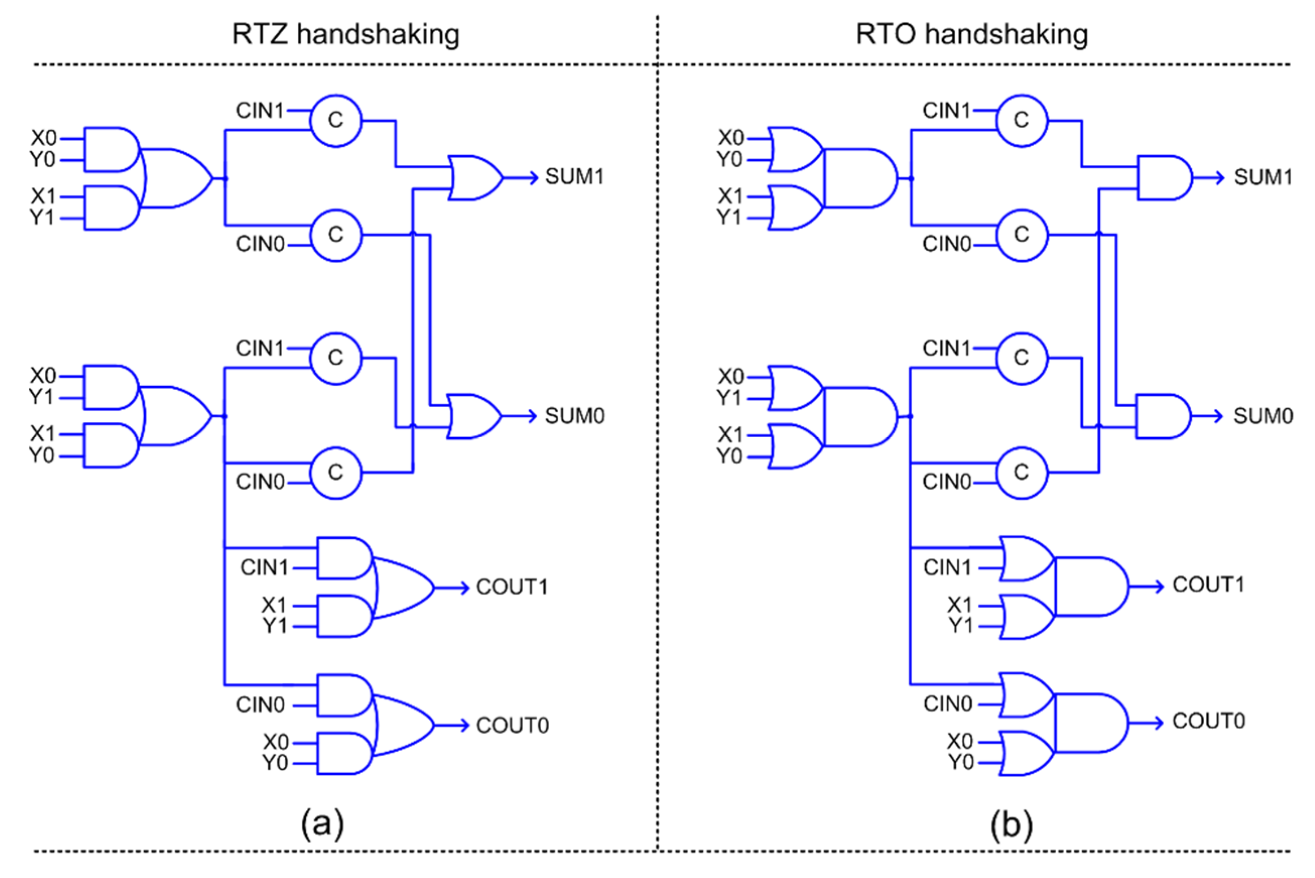
Early output full adder corresponding to RTZ and RTO handshaking are shown in
Figure 5a,b respectively, where (X1, X0), (Y1, Y0) and (CIN1, CIN0) represent its dual-rail inputs, and (SUM1, SUM0) and (COUT1, COUT0) represent its dual-rail outputs.
A QDI circuit corresponding to RTZ handshaking can be transformed into one that corresponds to RTO handshaking and vice versa by replacing all the gates, excepting the C-elements, by their respective duals—this principle has been proved in [
36], and an interested reader may refer to the same for the details.
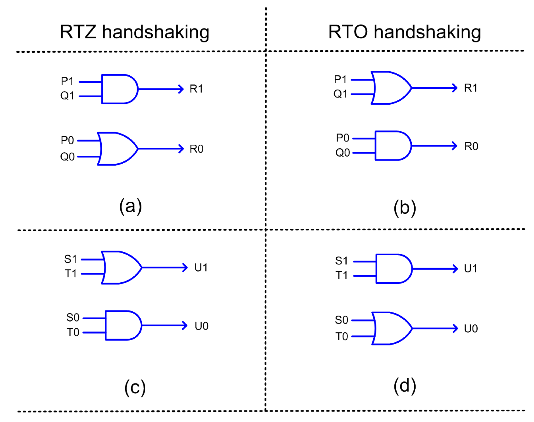
The accurate and approximate adders are QDI and are of early output type. The accurate part of LOAWA requires a cascade of early output full adders and a half adder. The accurate parts of LOA, APPROX5, HEAA, OLOCA, and HOERAA require a cascade of only early output full adders. The 2-input AND function shown in
Figure 3 is realized as an early output logic as shown in
Figure 6a,b, which correspond to RTZ and RTO handshaking. The 2-input OR function shown in
Figure 3 is realized as an early output logic as shown in
Figure 6c,d, which correspond to RTZ and RTO handshaking, respectively.
In the case of LOA, shown in
Figure 3b, 2-input AND and OR functions are used in the inaccurate part, and they were realized as early output circuits as shown in
Figure 6. In the case of LOAWA, only the 2-input OR function is used in the inaccurate part, and it was realized as shown in
Figure 6c,d.
With respect to APPROX5 (
Figure 3d), in the inaccurate part, the addend bits B
L–1 up to B
0 are directly forwarded as the respective sum bits viz. SUM
L–1 up to SUM
0, and A
L–2 up to A
0 are discarded. Only A
L–1 is given as the carry input to the accurate part in APPROX5. Given that a 22–10 input partition has been used for all the approximate adders considering a digital image processing application, therefore B
9 up to B
0 are forwarded as the respective sum bits SUM
9 up to SUM
0. This means that based on dual-rail encoding, B
91 up to B
01 are forwarded as SUM
91 up to SUM
01, and B
90 up to B
00 are forwarded as SUM
90 up to SUM
00, by using a non-inverting buffer for each encoded sum rail. (A
81, A
80) up to (A
01, A
00) are however discarded.
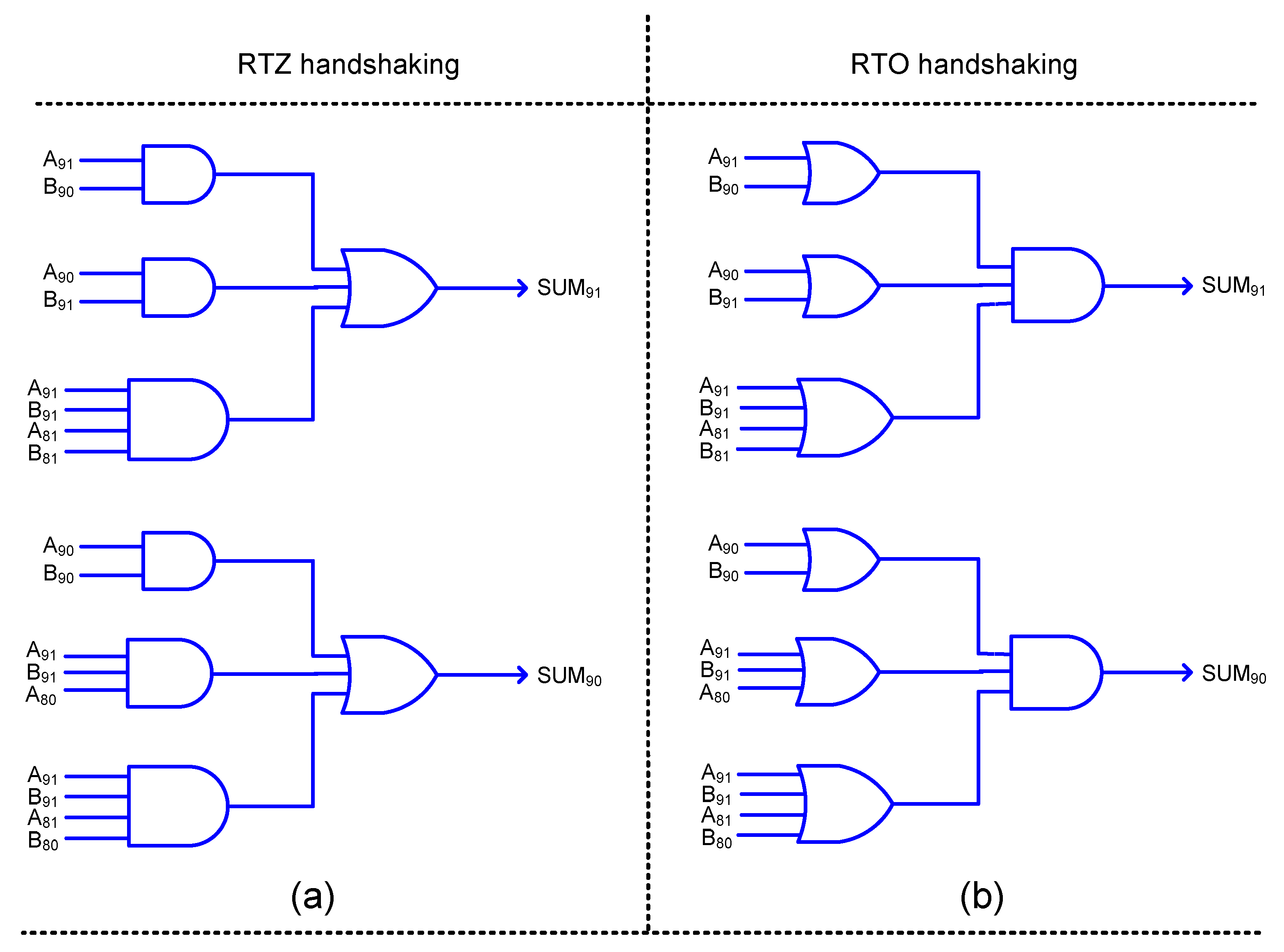
The logic corresponding to the most significant sum bit in the inaccurate part of HEAA (
Figure 3e) incorporates a 2:1 multiplexer. Multiplexers are generally not used in QDI circuit designs, because any signal transitions on their inputs may immediately result in signal transitions on their outputs and this may give rise to gate orphan(s). As already mentioned, gate orphan(s) should be avoided in QDI circuits. Hence, SUM
9 of HEAA, i.e., SUM
91 and SUM
90 are realized in early output style after logic simplification, as shown in
Figure 7a,b, which correspond to RTZ and RTO handshaking, respectively. The equations for SUM
91 and SUM
90 are given below.
In the case of OLOCA, the 2-input AND and OR functions are realized as shown in
Figure 6a,c with respect to RTZ handshaking, and as shown in
Figure 6b,d with respect to RTO handshaking. For the 22–10 input partition, and based on the OLOCA architecture, eight less significant sum bits in the inaccurate part are assigned a constant 1. This means that based on dual-rail encoding and RTZ handshaking, SUM
71 to SUM
01 should assume a constant 1 for the application of data and should assume 0 for the application of the spacer. This is realized by using a dedicated non-inverting buffer to connect each sum rail viz. SUM
71 to SUM
01 to the ACKIN signal. This would ensure that when ACKIN is 1 during the application of data, SUM
71 to SUM
01 will assume 1, and when ACKIN is 0 during the application of the spacer, SUM
71 to SUM
01 will assume 0. With respect to SUM
70 to SUM
00, they should always be 0. This is ensured by connecting each of these sum rails individually to TIEL (i.e., a tie-to-logic low) standard cells so that SUM
70 to SUM
00 will always remain 0. Considering RTO handshaking, SUM
71 to SUM
01 are individually connected to the ACKIN signal through dedicated non-inverting buffers, as done for RTZ handshaking. However, SUM
70 to SUM
00 are individually connected to TIEH (i.e., tie-to-logic high) standard cells so that SUM
70 to SUM
00 will always remain 1.
HOERAA, which is shown in
Figure 3g, is similar to OLOCA, with respect to the assignment of a constant one to the less significant sum bits SUM
7 to SUM
0. Hence, the circuits used for OLOCA with respect to these eight less significant sum bits are maintained the same for HOERAA for RTZ and RTO handshaking. Considering the most significant sum bit in the inaccurate part of HOERAA viz. SUM
9, again a 2:1 multiplexer is involved as is the case with HEAA discussed earlier. Therefore, SUM
9 of HOERAA, i.e., SUM
91 and SUM
90 after dual-rail encoding, was realized in an early output style after logic simplification, as described for HEAA, and this is shown in
Figure 8a,b with respect to RTZ and RTO handshaking.
4. Implementation Results
Accurate and approximate 32-bit adders were realized as QDI circuits using a 32/28-nm CMOS technology [
37], corresponding to RTZ and RTO handshake schemes separately. As mentioned earlier, the approximate adders comprise a 22-bit accurate part and a 10-bit inaccurate part, as this input partition suits the digital image processing application. Excepting the 2-input C-element that was custom realized as shown in
Figure 2c, the remaining gates used to construct the adders were utilized from the standard cell library. A typical-case PVT specification with a recommended supply voltage of 1.05 V and an operating junction temperature of 25 °C was considered for the simulations. All the sum bits were assigned a fanout-of-4 (FO-4) drive strength. The functional simulations were performed by supplying about a thousand random input vectors to the adders at a latency of 5ns and their switching activity profile were saved as value change dump (.vcd) files. The .vcd files were then used to estimate the average power dissipation.
The forward latency of a QDI asynchronous circuit is equivalent to the critical path delay of a synchronous circuit, and it can be directly estimated. The reverse latency may be equal to or less than the forward latency. For example, if an adder is constructed using strong-indication full and half adders, then its forward latency and reverse latency will be the same, which is equal to the worst-case delay. On the other hand, supposing if an adder is constructed using early output full and half adders, and if quasi-delay-insensitivity is maintained, then its forward latency would be data-dependent and its reverse latency would be a constant, which equates to the sum of the propagation delays of only two adjacent full adders. Since we used early output full adder and early output half adder to realize the accurate adder and the accurate parts of the approximate adders; therefore, the reverse latency would be a bare minimum, which is equal to the sum of the propagation delays of just two full adders. The reverse latency is estimated based on the gate-level timing information generated by the static timing analyzer. Nevertheless, as mentioned previously, the cycle time is the main timing parameter of interest in a QDI circuit, which is given by the sum of forward and reverse latencies. The forward latency, cycle time and area are given in
Table 1 for the accurate and approximate QDI adders with respect to RTZ and RTO handshaking.
A well-known low power figure-of-merit for a digital logic design is the power-delay product [
38], which is also called, energy. We are interested in estimating the delay, energy, and area, because approximate computing has the potential to enable simultaneous optimizations of all these design metrics compared to accurate computing. In synchronous circuits, the delay refers to the critical path delay, whereas in QDI asynchronous circuits, the delay refers to the cycle time. This is because in a QDI circuit, the cycle time defines the operating speed. The energy of QDI circuits is the product of power and cycle time, which is also given in
Table 1 for the RTZ and RTO handshake schemes.
Some general inferences can be drawn from
Table 1. Firstly, we see that compared to the accurate adder, the approximate adders have less cycle time, occupy less area, and are more energy-efficient—this is true for both RTZ and RTO handshaking. The accurate adder is 32 bits in size, whereas the accurate part of the approximate adders is only 22 bits in size. Moreover, there is either no connection or just a small logical connection between the accurate and inaccurate parts of the approximate adders, depending upon their architectures. The reduced size of the accurate part of approximate adders reduces the forward latency of the approximate adders, although the reverse latency of the accurate adder and the approximate adders are practically the same, which is equal to the propagation delays of two adjacent full adders. The inaccurate parts of the approximate adders have reduced logic compared to the accurate adder, and, as a result, the approximate adders require less area for implementation compared to the accurate adder. Eventually, the approximate adders are more energy-efficient compared to the accurate adder, and this is mainly due to a significant reduction in their cycle time. Secondly, the RTO handshaking consistently leads to reductions in cycle time, area, and energy, compared to RTZ handshaking. This has been discussed in prior works [
35,
39], where it was noted that, for QDI multipliers and adders, RTO handshaking enables better reductions in the design metrics compared to RTZ handshaking.
Among the approximate adders, LOAWA has the least cycle time, area, and energy for both RTZ and RTO handshaking. However, LOAWA does not have reduced error metrics compared to its counterparts, as will be discussed in the next section. Further, LOAWA did not lead to a better digital image processing result compared to its counterparts. Excluding LOAWA, all the other approximate adders have the same cycle time. In the case of LOAWA, there is no carry input to the accurate part and so an early output half adder can be used for the addition of the least significant input bit-pair in the accurate part. For the other approximate adders, there is a carry input given to their accurate part, and, hence, an early output full adder has to be used for the addition of the least significant input bit-pair including the incoming carry in the accurate part. The critical path delay of the early output half adder shown in
Figure 4a is equal to the propagation delay of a 2-input AND or OR gate, whereas the critical path delay of the early output full adder shown in
Figure 5a is equal to the sum of the propagation delays of two AO22 complex gates. This is the reason why LOAWA has a relatively reduced forward latency and cycle time, because it has an early output half adder in the least significant bit position of the accurate part, while its counterparts have an early output full adder in the same bit position, thus experiencing more latency and resulting in a somewhat higher cycle time. Excluding LOAWA, all the other approximate adders have the same cycle time, and, among these, HOERAA has reduced error metrics and, thus, facilitates better digital image processing, as will be discussed in the next section. The area and energy metrics of HOERAA and the other approximate adders (excluding LOAWA) are rather comparable, and there is no significant difference.
It is noted from
Table 1 that, based on RTZ handshaking, HOERAA reports a 19.7% reduction in cycle time, a 12.5% reduction in area, and an 17.7% reduction in energy, compared to the accurate adder. Based on RTO handshaking, HOERAA achieves an 18.7% reduction in cycle time, a 12.4% reduction in area, and a 16.6% reduction in energy compared to the accurate adder.
5. Error Metrics of Approximate Adders
The mean absolute error (MAE), also called the mean error distance, and the root mean square error (RMSE) are popular metrics often used in approximate computing [
40]. To estimate these error metrics for the approximate adders Python models of accurate and approximate adders were developed. A 32-bit addition would have a total of 2
64 distinct input vectors, which is computationally intensive to consider. Hence, we generated one million random input vectors, and supplied them to the accurate and approximate adders. For each input supplied, the absolute difference between the sum produced by an approximate adder and the sum produced by the accurate adder was calculated, which is also called the error magnitude. The error magnitude may be positive or negative or nil. The absolute error was computed individually for each approximate adder for each input vector supplied, and the mean of the absolute errors corresponding to a million random input vectors was calculated using Equation (3). The RMSE was calculated using Equation (4). MAE and RMSE calculated for the approximate adders are given in
Table 2. From
Table 2, it is seen that HOERAA has almost the same MAE as HEAA. However, HOERAA has 8.6% reduced RMSE compared to HEAA. Hence, in terms of the error metrics, HOERAA is preferable to its counterparts. The reduced MAE and RMSE of HOERAA leads to better digital image processing results, with an improved signal-to-noise ratio compared to the other approximate adders, and this shall be discussed in the next section.
In the above equations, ‘N’ denotes the adder size, ‘e’ is the error distance which is the absolute difference between the accurate and approximate adder sums, ‘P’ denotes the probability of an error value occurrence, and ‘δ’ is the set of all error values.
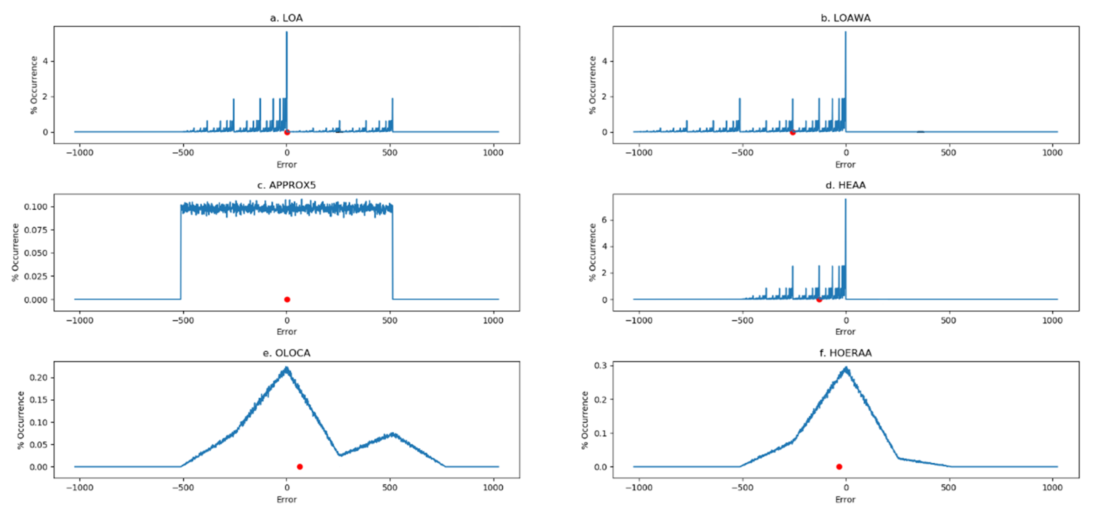
To analyze how HOERAA achieves reduced error metrics compared to its counterparts, we worked out the error distribution of the approximate adders, which is shown in
Figure 9. The error distribution curve is a plot of the error magnitudes (given in the
X-axis) as a function of their percentage occurrence (given in the
Y-axis), corresponding to the application of a million random input vectors. The absolute difference between the sum produced by an approximate adder and the sum produced by the accurate adder for an input vector may result in zero or a positive or a negative value. A red dot is used to represent the average of the absolute errors calculated for the approximate adders. Importantly, it is noted from
Figure 9 that among the approximate adders, APPROX5 and HOERAA have a rather symmetric error distribution about zero. However, the error magnitude of APPROX5 remains constantly high for several input vectors, but the error magnitude of HOERAA gradually increases towards zero, and then gradually decreases away from zero. HOERAA has the peak error for only a few input vectors compared to APPROX5, which has the peak error for several input vectors. This explains why MAE and RMSE of HOERAA are lesser than MAE and RMSE of APPROX5. In the case of HOERAA, the slope of the error distribution curve in the negative error direction is slightly greater than the slope of the error distribution in the positive error direction, so the average of the absolute errors is tilted towards the negative error direction. Among the approximate adders, HOERAA resembles a Gaussian error distribution, and HOERAA has reduced error metrics compared to the other approximate adders, as seen in
Table 2. This suggests that HOERAA is better suited for practical applications.
6. Digital Image Processing Results
To evaluate the practical usefulness of HOERAA and to compare its performance with the other approximate adders, we considered a digital image processing application. Many digital images with a spatial resolution of 512 × 512 and a grayscale resolution of 8-bits were used for the experimentation. We consider two images viz
lena and
cameraman here for illustration. We took an original image and then reconstructed it after computing fast Fourier transform (FFT) and inverse FFT (IFFT), similar to what was done in [
41]. Integer FFT and IFFT computations were performed. In the FFT and IFFT computations, only the addition operation was performed accurately or approximately, while the multiplications were performed accurately. To perform accurate addition, we used the accurate adder and to perform approximate addition, we used the approximate adder architectures discussed in
Section 3 individually.
Digital image processing was performed in the following manner. First, an original image was translated into a matrix form, which was then processed by a standard, i.e., accurate system, which computed accurate FFT, and it was subsequently reconstructed by computing accurate IFFT. The standard FFT and IFFT computations were done using the accurate 32-bit adder. The same original image was then processed by an approximate system that computed approximate FFT, and the image was reconstructed by computing approximate IFFT. Approximate adders of size 32-bits, which comprise a 22-bit accurate part and a 10-bit inaccurate part, processed the addition operations of approximate FFT and IFFT computations. The approximate additions involved in FFT and IFFT computations correspond to the approximate adder architectures discussed in
Section 3. The inputs given to the FFT were scaled up by a constant integer, i.e., 47, and the outputs of the IFFT were scaled down by the same constant to ensure that there is no data loss or overflow during the computation. The digital images
lena and
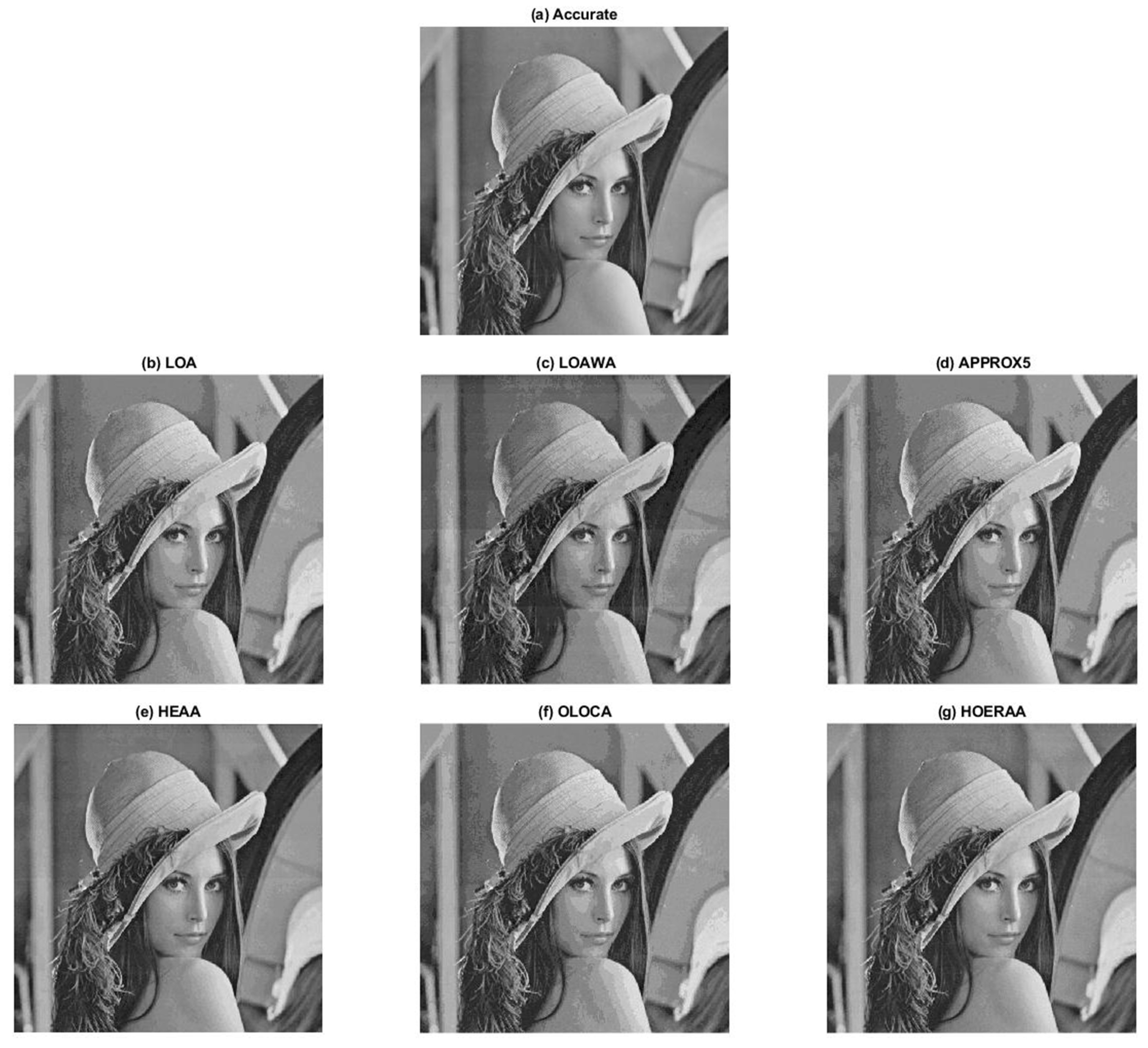
cameraman reconstructed through accurate and approximate FFT and IFFT computations are shown in
Figure 10 and
Figure 11, respectively.
The
lena images resulting from the use of the accurate adder is shown in
Figure 10a, and the approximate adders are shown in
Figure 10b–g. In the images, considerable shaded regions are visible in
Figure 10b–d,f, while only small grains are seen in
Figure 10e,g upon a close inspection.
The
cameraman images resulting from the use of the accurate adder is shown in
Figure 11a and the approximate adders are shown in
Figure 11b–g. In the images, considerable shaded regions are visible in
Figure 11b–d,f, moderate shades are visible in
Figure 11e, and only slight shades are seen in
Figure 11g.
The peak signal-to-noise ratio (PSNR) is a popular figure-of-merit that is widely used in digital signal processing [
42], and we estimated the PSNR for all the reconstructed images. A high PSNR is preferred, which implies less noise or distortion. Understandably, PSNR is infinite for the image reconstructed using the accurate adder, and this is because no error (noise) is introduced in the accurate computation.
The PSNR of
lena images processed using approximate FFT and IFFT by utilizing different approximate adders is as follows:
Figure 10b (LOA)—32.5795;
Figure 10c (LOAWA)—24.919;
Figure 10d (APPROX5)—31.8115;
Figure 10e (HEAA)—30.684;
Figure 10f (OLOCA)—32.1831; and
Figure 10g (HOERAA)—33.1214.
The PSNR of
cameraman images processed using approximate FFT and IFFT by utilizing different approximate adders is as follows:
Figure 11b (LOA)—32.1966;
Figure 11c (LOAWA)—25.0872;
Figure 11d (APPROX5)—31.306;
Figure 11e (HEAA)—30.68;
Figure 11f (OLOCA)—31.8063; and
Figure 11g (HOERAA)—32.73.
With respect to digital image processing involving approximate computing, besides PSNR, the structural similarity index metric (SSIM) [
42] was also estimated in some of the literature [
43]. While PSNR quantifies the absolute error, SSIM quantifies the perceived quality of digital images in terms of the perceived change in structural information compared to a distortion-free image, which is kept as the reference. Here, we measure the SSIM for images reconstructed using different approximate adders by treating the image reconstructed using the accurate adder as the reference.
SSIM for
lena images reconstructed through approximate FFT and IFFT by involving approximate additions is given as follows:
Figure 9b (LOA)—0.83993;
Figure 9c (LOAWA)—0.82568;
Figure 9d (APPROX5)—0.83265;
Figure 9e (HEAA)—0.9323;
Figure 9f (OLOCA)—0.83437; and
Figure 9g (HOERAA)—0.91539. SSIM for
cameraman images reconstructed through approximate FFT and IFFT by involving approximate additions is given as follows:
Figure 10b (LOA)—0.84435;
Figure 10c (LOAWA)—0.82436;
Figure 10d (APPROX5)—0.83639;
Figure 10e (HEAA)—0.92805;
Figure 10f (OLOCA)—0.84416; and
Figure 10g (HOERAA)—0.91308.
From
Figure 9 and
Figure 10, it is seen that HOERAA enables a better reproduction of the images compared to the other approximate adders given the higher PSNR for the images reproduced using HOERAA compared to the PSNR of the images reproduced using the other approximate adders. However, HEAA is quite comparable to HOERAA. In terms of SSIM, HEAA is slightly better than HOERAA although their SSIM values are rather close.
Besides
lena and
cameraman, which were used for illustration, many other digital images such as
woman_with_dark_hair,
barbara,
Einstein,
boat,
lake, and
peppers_gray were also considered for processing in the same manner as mentioned previously. PSNR and SSIM were also estimated for these images, and they are given in
Table 3 and
Table 4.
Table 3 and
Table 4 show a consistent trend in the performance characteristics of the approximate adders. From
Table 3, it is seen that HOERAA reports a higher PSNR compared to the other approximate adders based on experimentation with many digital images, as was noted for
lena and
cameraman earlier—this is thanks to its somewhat close to a Gaussian error distribution. From
Table 4, it is seen that HEAA reports greater SSIM compared to the other approximate adders for the different images, which is consistent with the observation made for
lena and
cameraman earlier. However, HOERAA is still comparable, and its SSIM is close to the SSIM of HEAA for all the images considered for processing.


