Manufacturing of Polymeric Substrates with Copper Nanofillers through Laser Stereolithography Technique

 , , ,
, , , 
Abstract
1. Introduction
2. Experimental Details
2.1. Materials and Methods
2.2. Characterization Techniques
3. Results and Discussions
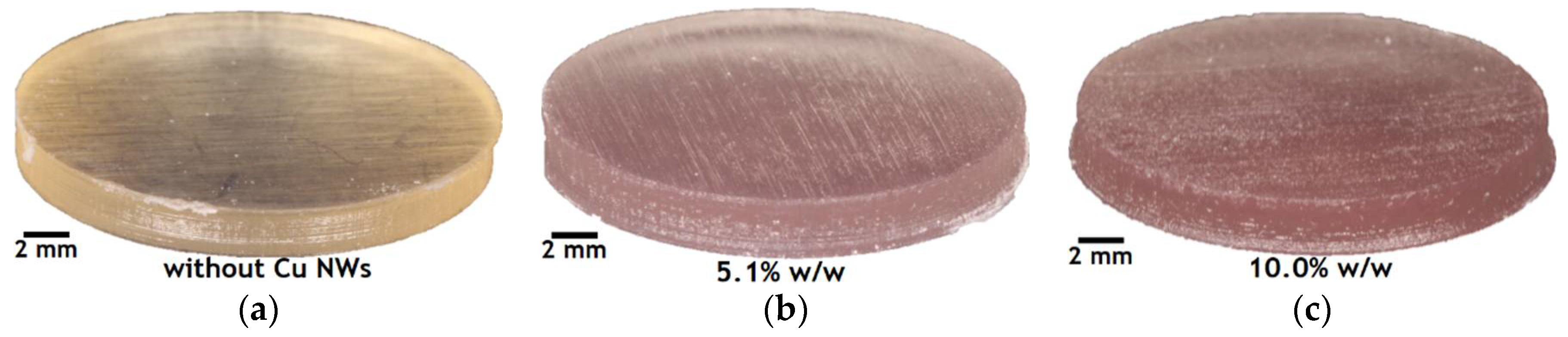
3.1. General Issues
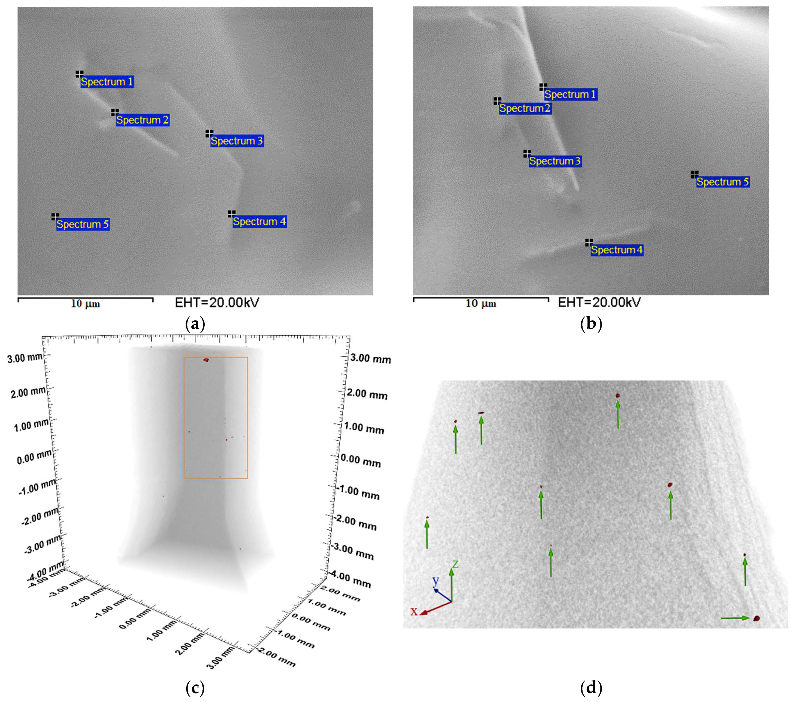
3.2. Morphology
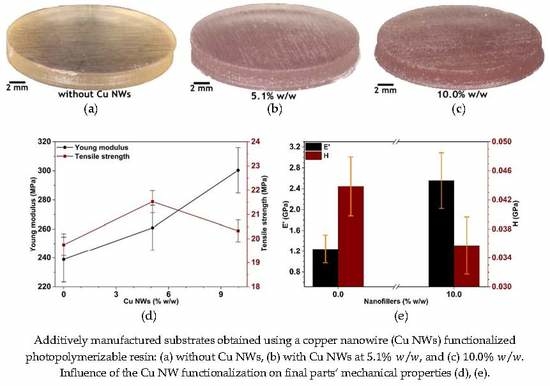
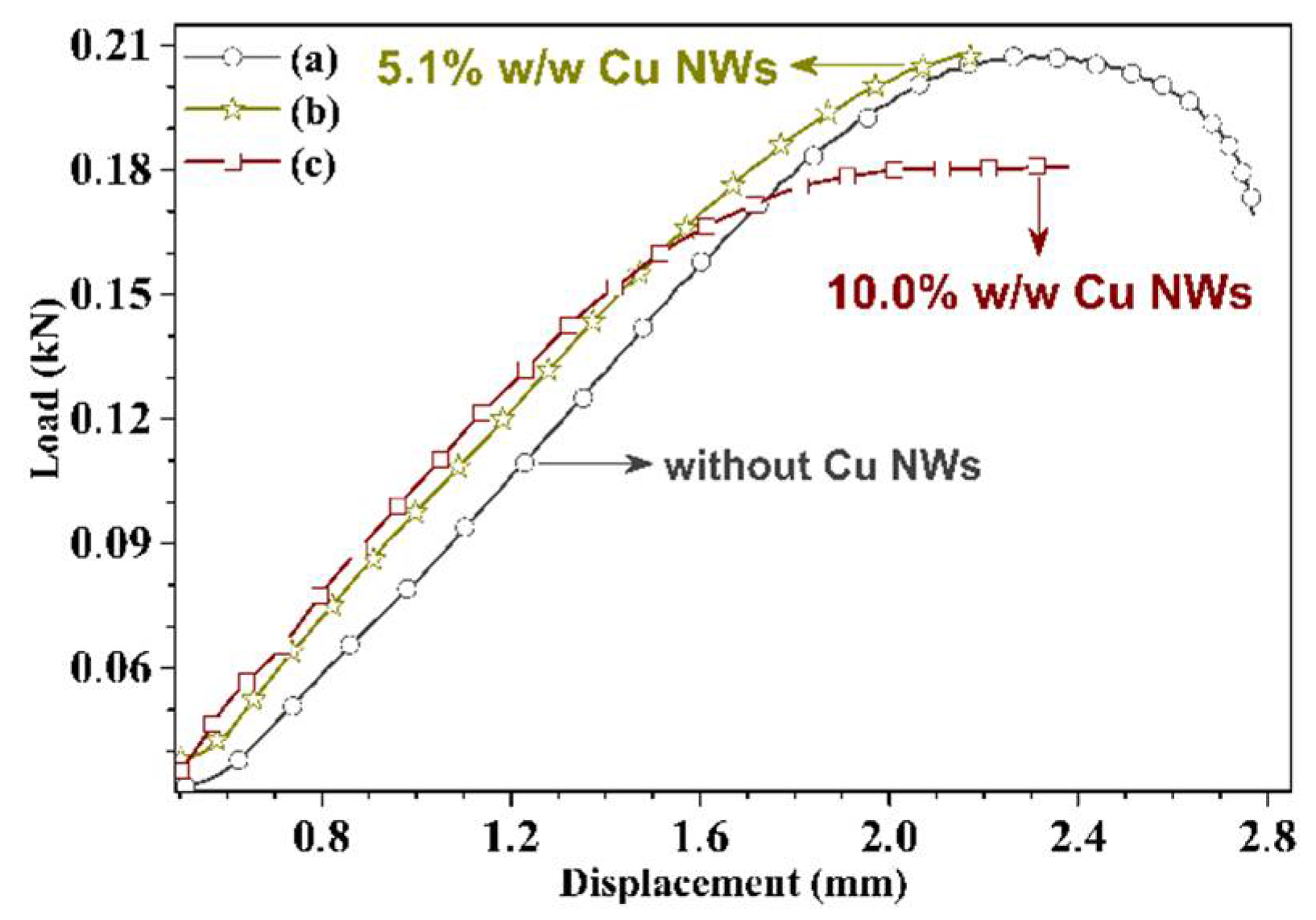
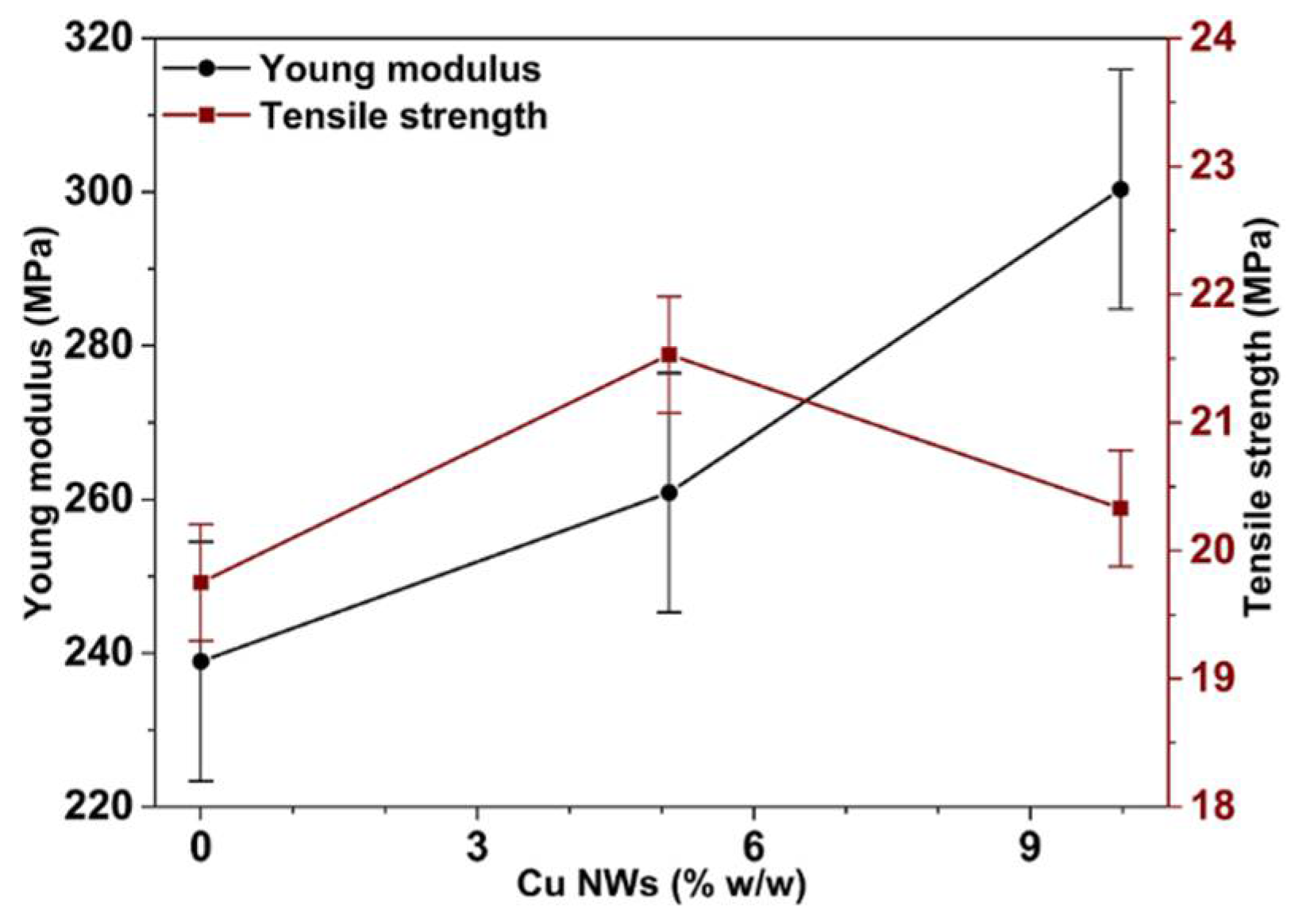
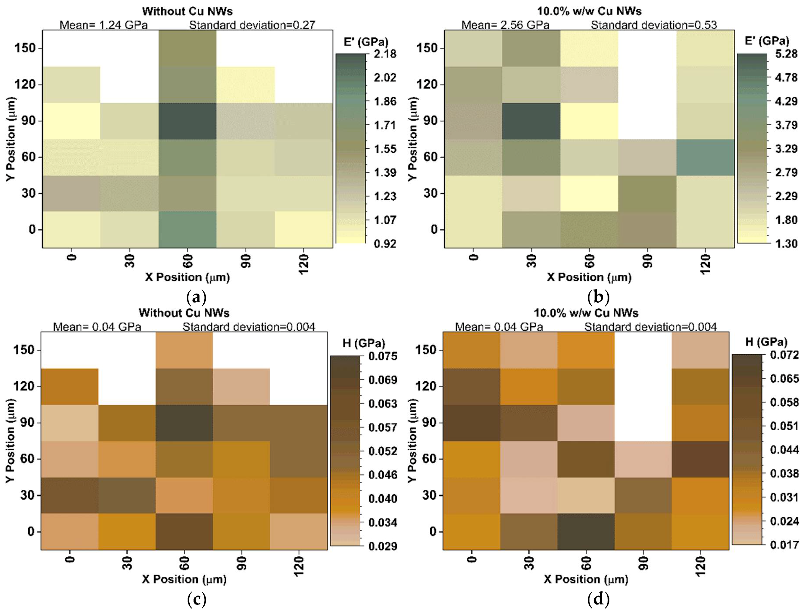
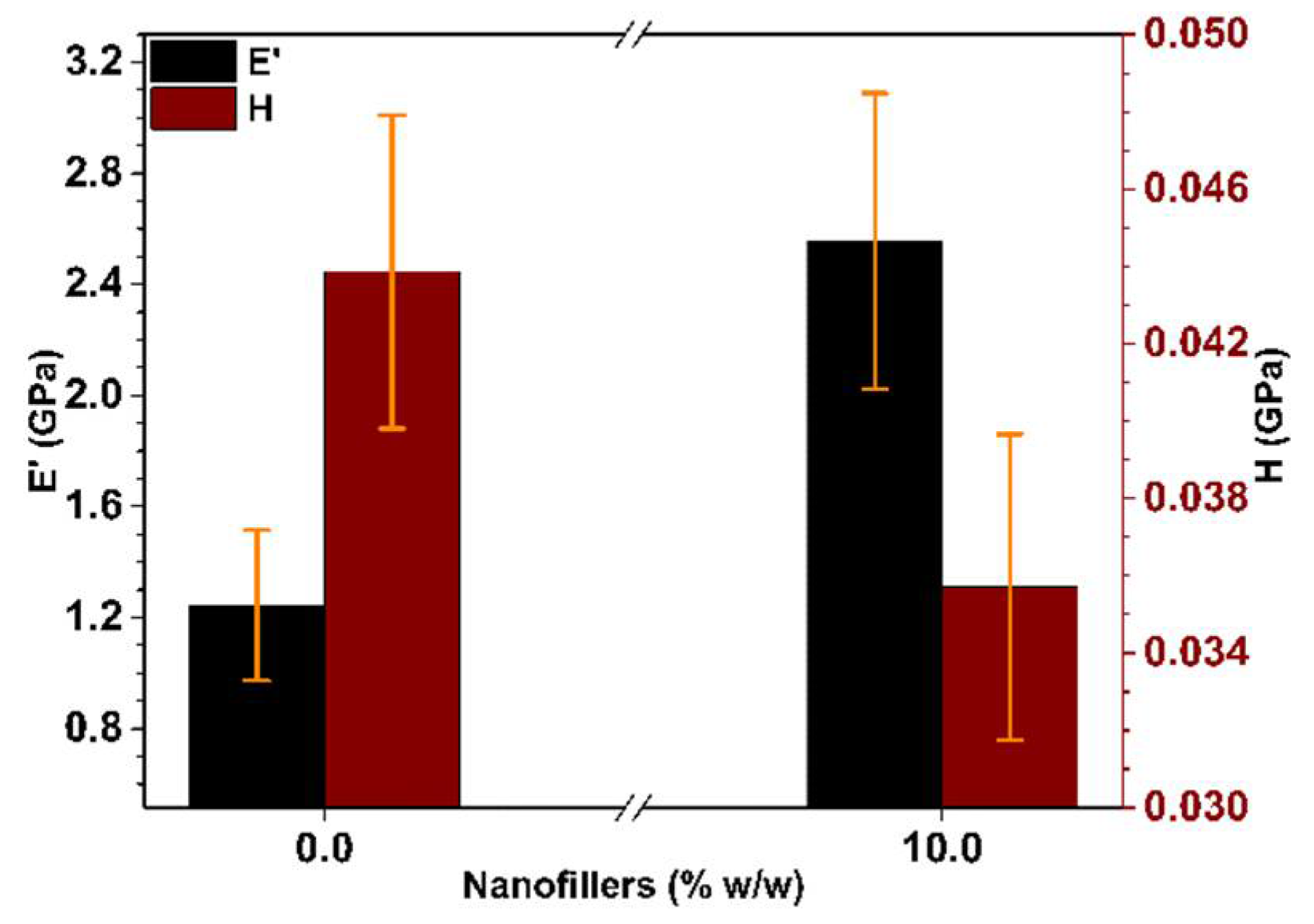
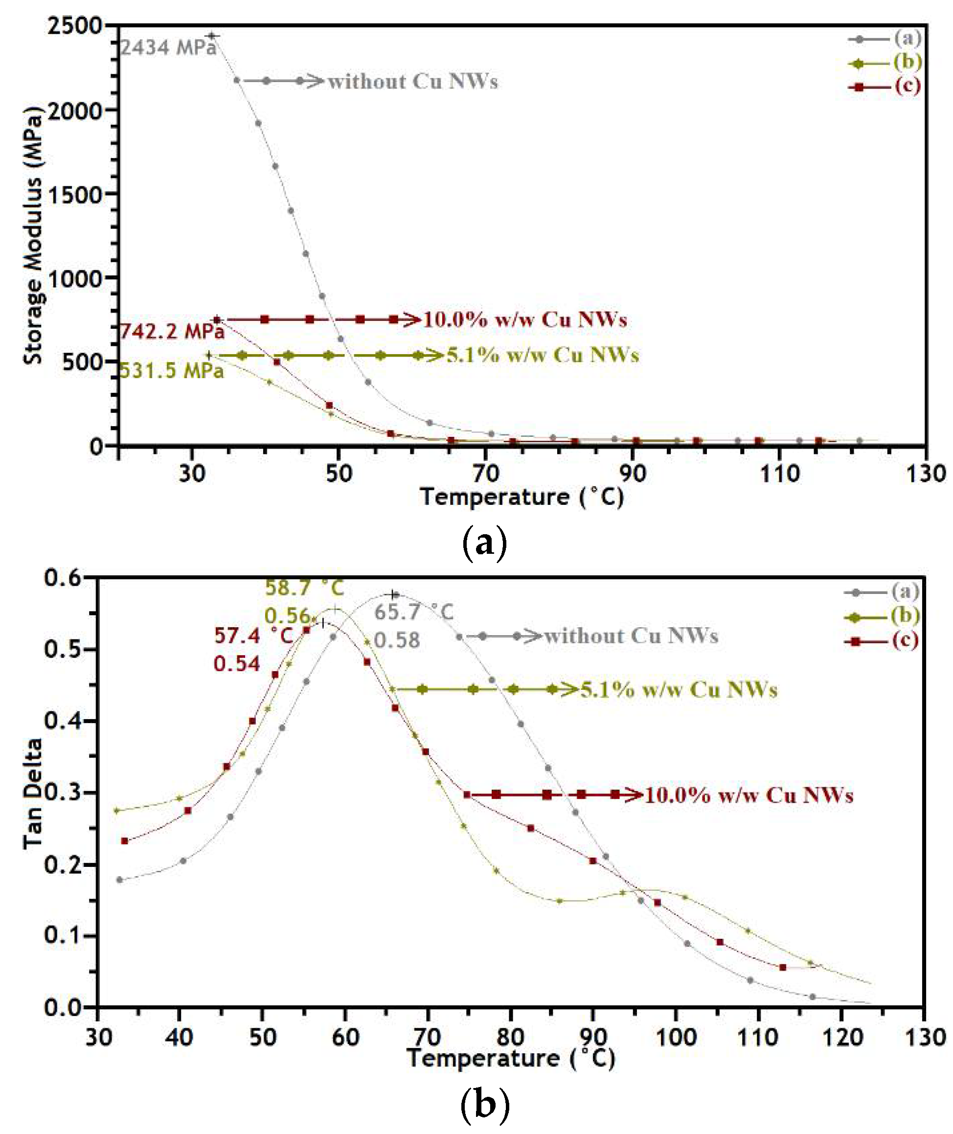
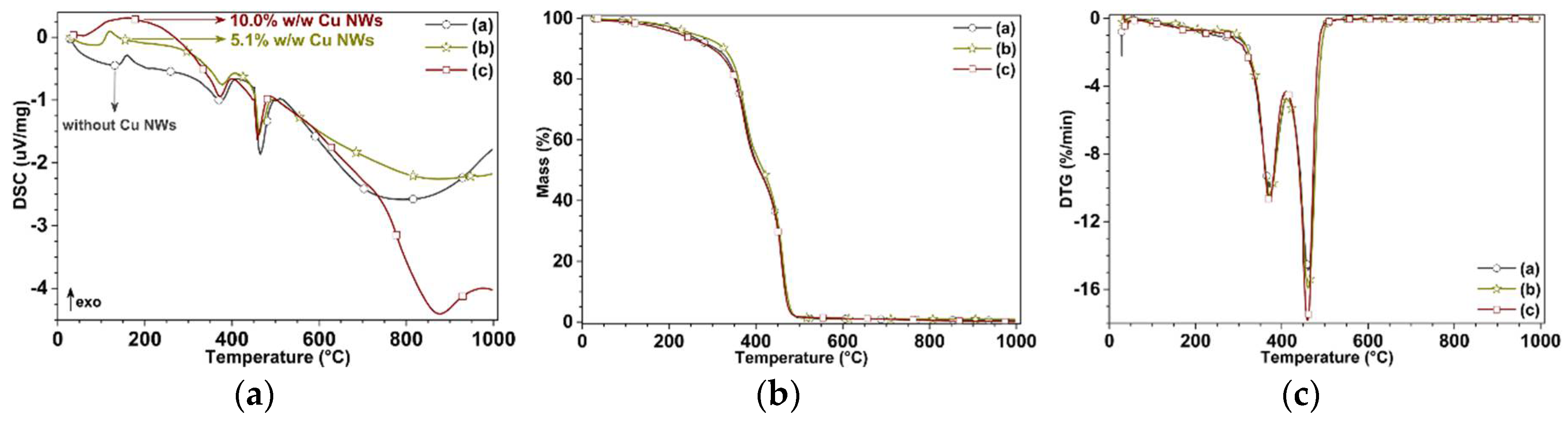
3.3. Mechanical and Thermal Performance
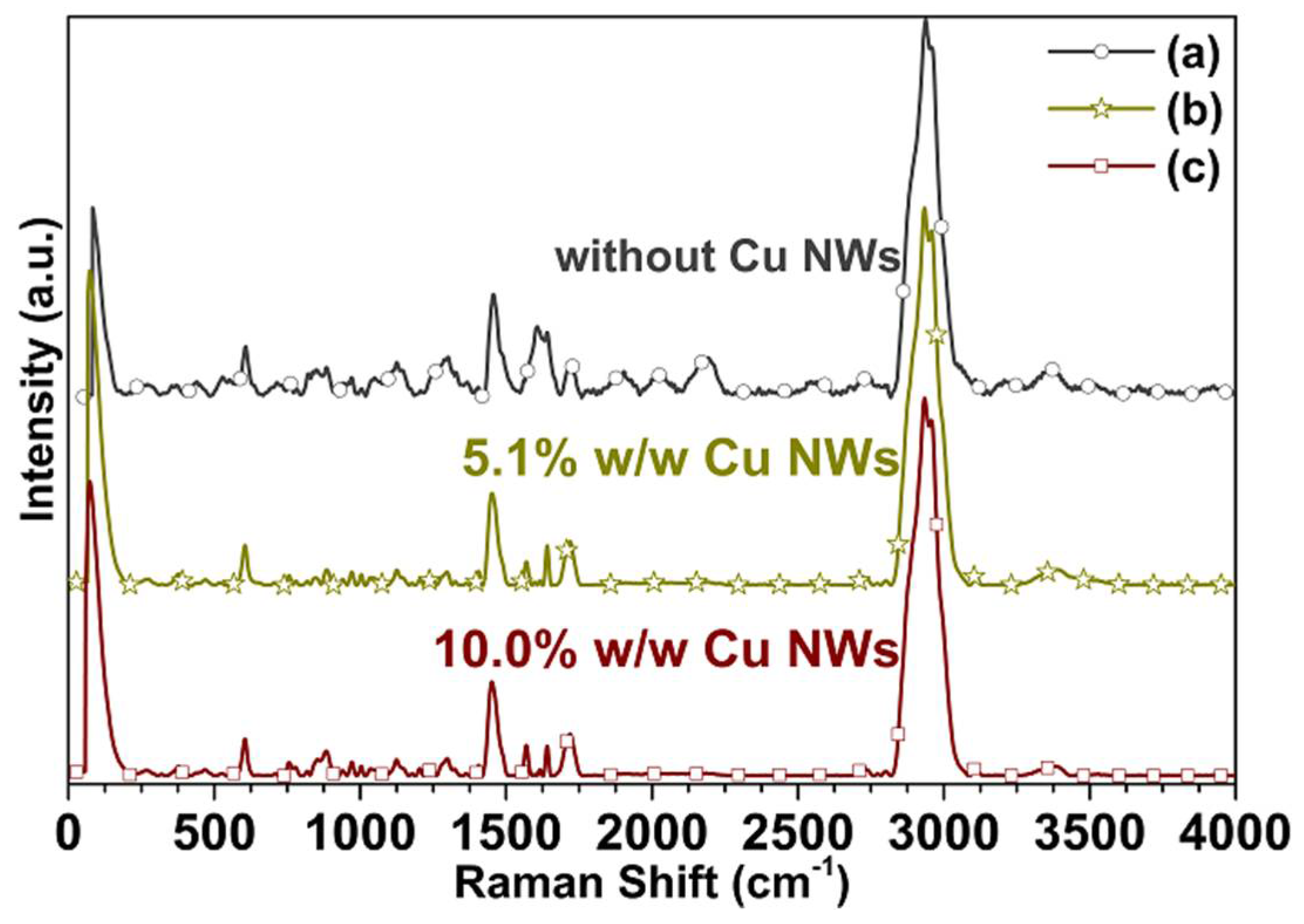
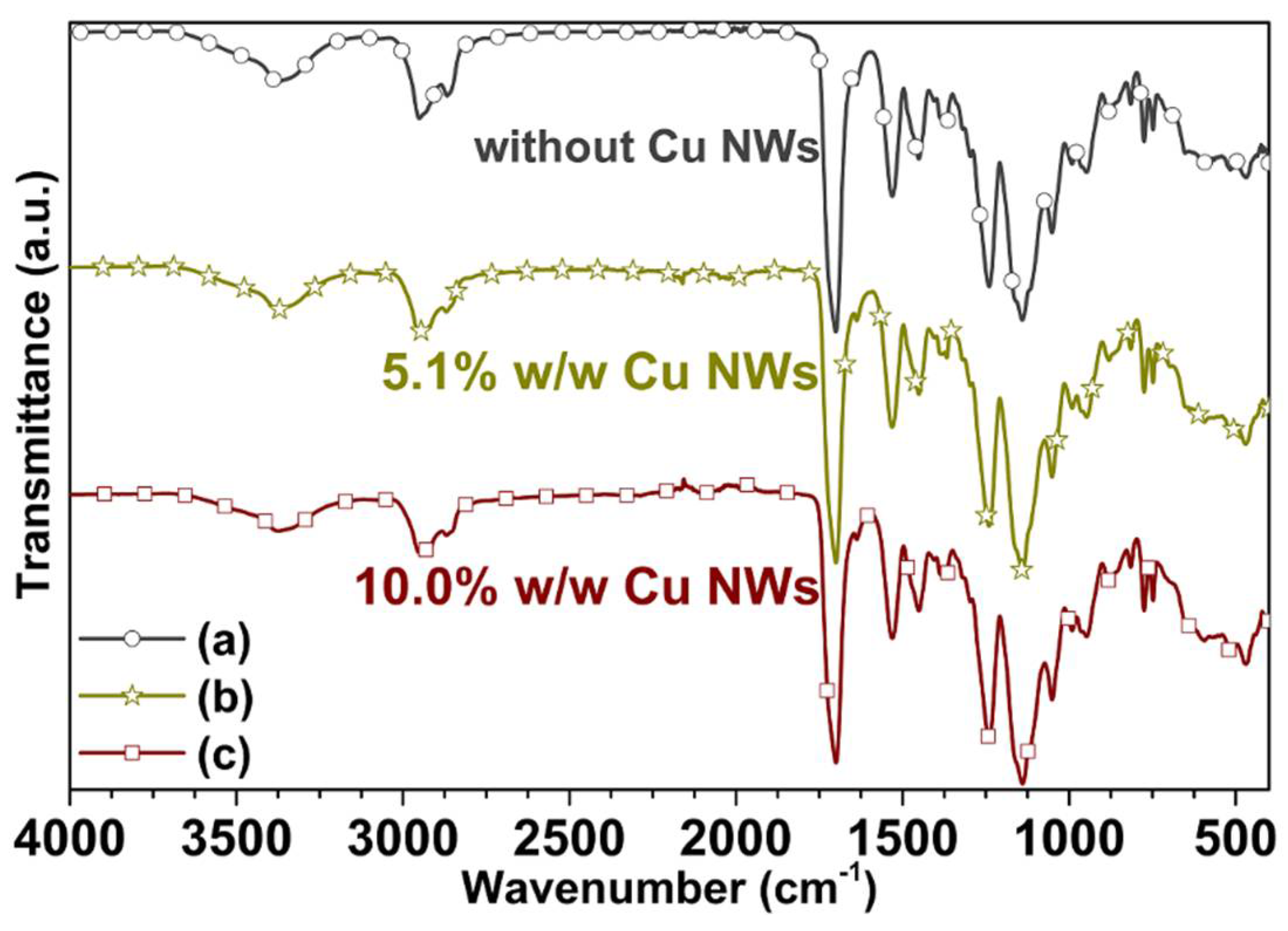
3.4. Spectroscopic Characterization
4. Conclusions
Author Contributions
Funding
Acknowledgments
Conflicts of Interest
References
- Ford, S.; Despeisse, M. Additive manufacturing and sustainability: An exploratory study of the advantages and challenges. J. Clean. Prod. 2016, 137, 1573–1587. [Google Scholar] [CrossRef]
- Mondschein, R.J.; Kanitkar, A.; Williams, C.B.; Verbridge, S.S.; Long, T.E. Polymer structure-property requirements for stereolithographic 3D printing of soft tissue engineering scaffolds. Biomaterials 2017, 140, 170–188. [Google Scholar] [CrossRef] [PubMed]
- Brennan-Craddock, J.; Brackett, D.; Wildman, R.; Hague, R. The design of impact absorbing structures for additive manufacture. J. Phys. Conf. Ser. 2012, 382, 1–7. [Google Scholar] [CrossRef]
- Wendel, B.; Rietzel, D.; Kühnlein, F.; Feulner, R.; Hulder, G.; Schmachtenberg, E. Additive processing of polymers. Macromol. Mater. Eng. 2008, 293, 799–809. [Google Scholar] [CrossRef]
- V-Niño, E.D.; Endrino-Armenteros, J.L.; Estupiñan-Duran, H.A.; Pérez-Gutiérrez, B.; Díaz-Lantada, A. Caracterización microscópica de texturas superficiales fabricadas aditivamente mediante estereolitografía laser. Respuestas 2016, 21, 37–47. [Google Scholar] [CrossRef]
- Kruth, J.P.; Froyen, L.; van Vaerenbergh, J.; Mercelis, P.; Rombouts, M.; Lauwers, B. Selective laser melting of iron-based powder. J. Mater. Process. Technol. 2004, 149, 616–622. [Google Scholar] [CrossRef]
- Yadroitsev, I.; Bertrand, P.; Smurov, I. Parametric analysis of the selective laser melting process. Appl. Surf. Sci. 2007, 253, 8064–8069. [Google Scholar] [CrossRef]
- Bremen, S.; Meiners, W.; Diatlov, A. Selective laser melting: A manufacturing technology for the future? Laser Tech. J. 2012, 9, 33–38. [Google Scholar] [CrossRef]
- Maruo, S.; Ikuta, K. Submicron stereolithography for the production of freely movable mechanisms by using single-photon polymerization. Sens. Actuators A Phys. 2002, 100, 70–76. [Google Scholar] [CrossRef]
- Sun, C.; Fang, N.; Wu, D.M.; Zhang, X. Projection micro-stereolithography using digital micro-mirror dynamic mask. Sens. Actuators A Phys. 2005, 121, 113–120. [Google Scholar] [CrossRef]
- Pham, A.T.; Kim, D.; Lim, T.; Park, S.; Yang, D.; Lee, K. Three-Dimensional SiCN ceramic microstructures via nano-stereolithography of inorganic polymer photoresists. Adv. Funct. Mater. 2006, 16, 1235–1241. [Google Scholar] [CrossRef]
- Bhushan, B.; Caspers, M. An overview of additive manufacturing (3D printing) for microfabrication. Microsyst. Technol. 2017, 23, 1117–1124. [Google Scholar] [CrossRef]
- American Society for Testing and Materials (ASTM). Standard Test Method for Tensile Properties of Plastics; ASTM D638-14; American Society for Testing and Materials: West Conshohocken, PA, USA, 2014. [Google Scholar]
- Lantada, A.D.; de Blas Romero, A.; Tanarro, E.C. Micro-vascular shape-memory polymer actuators with complex geometries obtained by laser stereolithography. Smart Mater. Struct. 2016, 25, 065018. [Google Scholar] [CrossRef]
- Wang, J.; Goyanes, A.; Gaisford, S.; Basit, A.W. Stereolithographic (SLA) 3D printing of oral modified-release dosage forms. Int. J. Pharm. 2016, 503, 207–212. [Google Scholar] [CrossRef] [PubMed]
- Lonne, Q.; Endrino, J.L.; Huang, Z. UV treatment of flexible copper nanowire mesh films for transparent conductor applications. Nanoscale Res. Lett. 2017, 12, 1–8. [Google Scholar] [CrossRef] [PubMed]
- Cohen, S.R.; Kalfon-Cohen, E. Dynamic nano-indentation by instrumented nano-indentation and force microscopy: A comparative review. Beilstein J. Nanotechnol. 2013, 4, 815–833. [Google Scholar] [CrossRef] [PubMed]
- Grzesik, M.; Skrzypek, J.; Witczak, M. Kinetic models for esterification of methacrylic acid using n-propanol and isopropanol. Stud. Surf. Sci. Catal. 2001, 133, 541–545. [Google Scholar]
- Lal, J.; Green, R. The preparation of some esters of methacrylic acid. J. Org. Chem. 1955, 20, 1030–1033. [Google Scholar] [CrossRef]
- Crosby, A.J.; Lee, J.-Y. Polymer nanocomposites: The “nano” effect on mechanical properties. Polym. Rev. 2007, 47, 217–229. [Google Scholar] [CrossRef]
- Bansal, A.; Yang, H.; Li, C.; Benicewicz, B.C.; Kumar, S.K.; Schadler, L.S. Controlling the thermomechanical properties of polymer nanocomposites by tailoring the polymer-particle interface. J. Polym. Sci. Part B Polym. Phys. 2006, 44, 2944–2950. [Google Scholar] [CrossRef]
- Ye, S.; Rathmell, A.R.; Chen, Z.; Stewart, I.E.; Wiley, B.J. Metal nanowire networks: The next generation of transparent conductors. Adv. Mater. 2014, 26, 6670–6687. [Google Scholar] [CrossRef] [PubMed]
- Cnudde, V.; Jacobs, P.J.S. Monitoring of weathering and conservation of building materials through non-destructive X-ray computed microtomography. Environ. Geol. 2004, 46, 477–485. [Google Scholar] [CrossRef]
- Hong, G.; Choi, S. Rapid self-sealing of cracks in cementitious materials incorporating superabsorbent polymers. Constr. Build. Mater. 2017, 143, 366–375. [Google Scholar] [CrossRef]
- Garcea, S.C.; Sinclair, I.; Spearing, S.M.; Withers, P.J. Mapping fibre failure in situ in carbon fibre reinforced polymers by fast synchrotron X-ray computed tomography. Compos. Sci. Technol. 2017, 149, 81–89. [Google Scholar] [CrossRef]
- Altun, V.; Remigy, J.C.; Vankelecom, I.F.J. UV-cured polysulfone-based membranes: Effect of co-solvent addition and evaporation process on membrane morphology and SRNF performance. J. Membr. Sci. 2017, 524, 729–737. [Google Scholar] [CrossRef]
- Struzynska-Piron, I.; Loccufier, J.; Vanmaele, L.; Vankelecom, I.F.J. Synthesis of solvent stable polymeric membranes via UV depth-curing. Chem. Commun. 2013, 49, 11494–11496. [Google Scholar] [CrossRef] [PubMed]
- Sandler, J.; Shaffer, M.S.P.; Prasse, T.; Bauhofer, W.; Schulte, K.; Windle, A.H. Development of a dispersion process for carbon nanotubes in an epoxy matrix and the resulting electrical properties. Polymer 1999, 40, 5967–5971. [Google Scholar] [CrossRef]
- Xie, X.L.; Mai, Y.W.; Zhou, X.P. Dispersion and alignment of carbon nanotubes in polymer matrix: A review. Mater. Sci. Eng. R 2005, 49, 89–112. [Google Scholar] [CrossRef]
- Ma, P.C.; Siddiqui, N.A.; Marom, G.; Kim, J.K. Dispersion and functionalization of carbon nanotubes for polymer-based nanocomposites: A review. Compos. Part A 2010, 41, 1345–1367. [Google Scholar] [CrossRef]
- Chakraborty, A.K.; Plyhm, T.; Barbezat, M.; Necola, A.; Terrasi, G.P. Carbon nanotube (CNT)–epoxy nanocomposites: A systematic investigation of CNT dispersion. J. Nanopart. Res. 2011, 13, 6493–6506. [Google Scholar] [CrossRef]
- Gayle, A.J.; Cook, R.F. Mapping viscoelastic and plastic properties of polymers and polymer-nanotube composites using instrumented indentation. J. Mater. Res. 2016, 31, 2347–2360. [Google Scholar] [CrossRef] [PubMed]
- Jyotishkumar, P.; Pionteck, J.; Hassler, R.; George, S.M.; Cvelbar, U.; Thomas, S. Studies on stress relaxation and thermomechanical properties of Poly(acrylonitrile-butadiene-styrene) modified epoxy-amine systems. Ind. Eng. Chem. Res. 2011, 50, 4432–4440. [Google Scholar]
- Wei, X.; Li, D.; Jiang, W.; Gu, Z.; Wang, X.; Zhang, Z.; Sun, Z. 3D Printable Graphene Composite. Sci. Rep. 2015, 5, 1–7. [Google Scholar] [CrossRef] [PubMed]
- Doganay, D.; Coskun, S.; Kaynak, C.; Unalan, H.E. Electrical, mechanical and thermal properties of aligned silver nanowire/polylactide nanocomposite films. Compos. Part B 2016, 99, 288–296. [Google Scholar] [CrossRef]
- Hua, M.Z.; Feng, S.; Wang, S.; Lu, X. Rapid detection and quantification of 2,4-dichlorophenoxyacetic acid in milk using molecularly imprinted polymers–surface-enhanced Raman spectroscopy. Food Chem. 2018, 258, 254–259. [Google Scholar] [CrossRef] [PubMed]
- Sessa, C.; Weiss, R.; Niessner, R.; Ivleva, N.P.; Stege, H. Towards a Surface Enhanced Raman Scattering (SERS) spectra database for synthetic organic colourants in cultural heritage. The effect of using different metal substrates on the spectra. Microchem. J. 2018, 138, 209–225. [Google Scholar] [CrossRef]
- Garcia-Rico, E.; Alvarez-Puebla, R.A.; Guerrini, L. Direct surface-enhanced Raman scattering (SERS) spectroscopy of nucleic acids: From fundamental studies to real-life applications. Chem. Soc. Rev. 2018, 47, 4909–4923. [Google Scholar] [CrossRef] [PubMed]
- Zhao, T.; Li, X.; Yu, R.; Zhang, Y.; Yang, X.; Zhao, X.; Wang, L.; Huang, W. Silicone–epoxy-based hybrid photopolymers for 3D printing. Macromol. Chem. Phys. 2018, 1700530, 1–10. [Google Scholar] [CrossRef]
- Weng, Z.; Zhou, Y.; Lin, W.; Senthil, T.; Wu, L. Structure-property relationship of nano enhanced stereolithography resin for desktop SLA 3D printer. Compos. Part A 2016, 88, 234–242. [Google Scholar] [CrossRef]


| Resin Type | Clear FLGPCL 02 | |||
| Type of additive | Without Additive | Cu NWs | ||
| Mass of the nano-additive solution (g) | N/A | |||
| Nano-additive mass (g) | N/A | |||
| Additive percentage (% w/w) * | N/A | |||
| Mixture time (min) | N/A | |||
| Substrate type | Cylindrical | Tensile testing | Cylindrical | Tensile testing |
| Quantity of printed substrates | ||||
| Printing time (min) | ||||
| Print resolution (µm) | ||||
| Number of layers | ||||
| Measurements from | Parameters | Substrate Type | ||
|---|---|---|---|---|
| Without Cu NWs | ||||
| CAD design | Radius () | |||
| Thickness () | ||||
| Volume () | ||||
| Mass * () | ||||
| Fabricated substrates | Radius () | |||
| Thickness () | ||||
| Volume () | ||||
| Mass () | ||||
| Density () | ||||
| Materials | Cost |
|---|---|
| Liquid resin | |
| Cu NWs | * |
| Element | Spectrum 1 | Spectrum 2 | Spectrum 3 | Spectrum 5 |
|---|---|---|---|---|
| At% | At% | At% | At% | |
| C k | ||||
| O k | ||||
| Cu k | - |
| Element | Spectrum 1 | Spectrum 3 | Spectrum 4 | Spectrum 5 |
|---|---|---|---|---|
| At% | At% | At% | At% | |
| C k | ||||
| O k | ||||
| Cu k | - |
| Cu NWs Content | Transition and Degradation Temperatures (°C) | ||
|---|---|---|---|
| Without Cu NWs | |||
© 2018 by the authors. Licensee MDPI, Basel, Switzerland. This article is an open access article distributed under the terms and conditions of the Creative Commons Attribution (CC BY) license (http://creativecommons.org/licenses/by/4.0/).
Share and Cite
V-Niño, E.D.; Díaz Lantada, A.; Lonne, Q.; Estupiñán Durán, H.A.; Mejía-Ospino, E.; Ramírez-Caballero, G.; Endrino, J.L. Manufacturing of Polymeric Substrates with Copper Nanofillers through Laser Stereolithography Technique. Polymers 2018, 10, 1325. https://doi.org/10.3390/polym10121325
V-Niño ED, Díaz Lantada A, Lonne Q, Estupiñán Durán HA, Mejía-Ospino E, Ramírez-Caballero G, Endrino JL. Manufacturing of Polymeric Substrates with Copper Nanofillers through Laser Stereolithography Technique. Polymers. 2018; 10(12):1325. https://doi.org/10.3390/polym10121325
Chicago/Turabian StyleV-Niño, Ely Dannier, Andrés Díaz Lantada, Quentin Lonne, Hugo Armando Estupiñán Durán, Enrique Mejía-Ospino, Gustavo Ramírez-Caballero, and José Luis Endrino. 2018. "Manufacturing of Polymeric Substrates with Copper Nanofillers through Laser Stereolithography Technique" Polymers 10, no. 12: 1325. https://doi.org/10.3390/polym10121325
APA StyleV-Niño, E. D., Díaz Lantada, A., Lonne, Q., Estupiñán Durán, H. A., Mejía-Ospino, E., Ramírez-Caballero, G., & Endrino, J. L. (2018). Manufacturing of Polymeric Substrates with Copper Nanofillers through Laser Stereolithography Technique. Polymers, 10(12), 1325. https://doi.org/10.3390/polym10121325