Article

Critical Evaluation of Organic Thin-Film Transistor Models

1
Institute of Solid State Physics, NAWI Graz, Graz University of Technology, Petersgasse 16, 8010 Graz, Austria
2
Max Planck Institute for Solid State Research, Heisenbergstr. 1, 70569 Stuttgart, Germany
3
Joanneum Research Materials, Institute for Surface Technologies and Photonics, Franz-Pichler-Straße 30, 8160 Weiz, Austria
*
Author to whom correspondence should be addressed.
Crystals 2019, 9(2), 85; https://doi.org/10.3390/cryst9020085
Submission received: 20 December 2018 / Revised: 23 January 2019 / Accepted: 2 February 2019 / Published: 6 February 2019
(This article belongs to the Special Issue Thin Film Transistor)

Abstract

:
The thin-film transistor (TFT) is a popular tool for determining the charge-carrier mobility in semiconductors, as the mobility (and other transistor parameters, such as the contact resistances) can be conveniently extracted from its measured current-voltage characteristics. However, the accuracy of the extracted parameters is quite limited, because their values depend on the extraction technique and on the validity of the underlying transistor model. We propose here a new approach for validating to what extent a chosen transistor model is able to predict correctly the transistor operation. In the two-step fitting approach we have developed, we analyze the measured current-voltage characteristics of a series of TFTs with different channel lengths. In the first step, the transistor parameters are extracted from each individual transistor by fitting the output and transfer characteristics to the transistor model. In the second step, we check whether the channel-length dependence of the extracted parameters is consistent with the underlying model. We present results obtained from organic TFTs fabricated in two different laboratories using two different device architectures, three different organic semiconductors and five different materials combinations for the source and drain contacts. For each set of TFTs, our approach reveals that the state-of-the-art transistor models fail to reproduce correctly the channel-length-dependence of the transistor parameters. Our approach suggests that conventional transistor models require improvements in terms of the charge-carrier-density dependence of the mobility and/or in terms of the consideration of uncompensated charges in the carrier-accumulation channel.

Graphical Abstract

1. Introduction

The fabrication of organic thin-film transistors (TFTs) has reached a level at which devices with excellent performance, small device-to-device variations, and smooth electrical characteristics with small hysteresis can routinely be provided [1,2,3,4]. These technological advances are significantly ahead of our current ability to reliably extract crucial transistor parameters. Such a reliable extraction procedure is desirable to design integrated circuits, to determine materials parameters, or to optimize the TFT fabrication process. The two most prominent of these transistor parameters are the charge-carrier mobility as a materials parameter and the contact resistance as an indicator for the quality of the contact-semiconductor interfaces. To extract these parameters from the measured current-voltage characteristics, the device operation and, hence, the electrical TFT characteristics must be understood in terms of these parameters.
In general, every parameter extraction approach requires a theoretical model for the transistor operation that provides the current-voltage relations on the basis of input parameters that properly account for the regime of operation (applied voltages), the materials properties, and the device geometry. While materials-related transistor parameters comprise, for example, the charge-carrier mobility and the permittivity of the gate dielectric, the most prominent geometry parameters are the channel length, the channel width, and the gate-dielectric thickness. Such theoretical models hold much promise of being able to associate correctly any changes in the current-voltage characteristics to changes in these transistor parameters. Hence, it is particularly desirable to utilize a theoretical transistor model that associates the drain current of the transistors to these parameters, preferably with a closed analytic expression. To obtain reliable and robust relations, it is customary to conceive of specific models for each class of TFTs by accounting, for example, for a particular transport mechanism [5,6] or particular geometry features, such as a small channel length [7]. The potential success of a theoretical model inherently relies on a set of preliminary assumptions that are guided by the device geometry and by the anticipated transport mechanism. For instance, in the presumably most prominent field-effect-transistor model, the gradual channel approximation, it is assumed that all mobile charges are confined to the interface between the semiconductor layer and the gate dielectric. Despite the many efforts to improve the transistor models in order to better comply with the measured electrical characteristics [8,9], the development of refined models is still in its infancy, as there are no reliable tools to validate the consistency between the prediction made by a given theoretical model and the measured current-voltage characteristics of the transistors.
Here, we propose a new approach for evaluating the adequateness of a suggested theoretical transistor model. Our approach is a two-step process that requires a set of transistors with different channel lengths. The two steps combine the benefits and overcome the drawbacks of the two classes of established extraction approaches, namely the “single transistor methods” and the “channel-length-scaling approaches” [10]. “Single transistor methods” seek to extract the parameters of an assumed transistor model from certain operation regimes in the output or/and transfer characteristics of an individual TFT [9,10,11,12,13], whereas in “channel-length-scaling approaches”, parameters are extracted from a series of nominally identical transistors that differ only in the channel length, by exploring the dependence of the transistor characteristics on the channel length from the perspective of the assumed model [14,15,16]. Neither of these two classes of established extraction approaches is able to validate reliably the consistency between the theoretical model and the measured current-voltage characteristics. For the “single transistor methods”, the consistency can, at best, be validated within the limited region from which the transistor parameters are extracted, and for the “channel-length-scaling approaches”, the deviations of the model predictions from the measured data are often hidden by unavoidable device-to-device variations.
The approach we present here combines fundamental aspects of these two classes of established parameter extraction methods. This combination allows us to go beyond existing extraction methods by enabling a reliable validation of the adequateness of the theoretical model underlying the extraction method. In the first step of our approach, the current-voltage characteristics of individual transistors are analyzed. We fit the entire set of measured data points of all output and transfer characteristics simultaneously to the underlying theoretical model. As pointed out by Deen et al. [17] and Fischer et al. [18], the simultaneous consideration of all available data points guarantees the best possible parameter set describing an individual transistor as a whole and eliminates the aforementioned ambiguity that arises from selecting certain regions of device operation. The extracted parameter set is then used to calculate the output and transfer characteristics I D ( V D S ) and I D ( V G S ) . By comparing the calculated and the measured current-voltage characteristics, we are able to perform an initial check of the validity of the underlying theoretical model. Furthermore, any deviations between the calculated and the measured characteristics can be analyzed in order to derive strategies for improving the underlying transistor model. If this check is successful and the calculated characteristics are in good agreement with the measured characteristics, we proceed to the second step of our approach in which we compare the individually-extracted fitting parameters of all devices with regard to their channel-length dependencies. The second step relies on the hypothesis that the transistor can be spatially separated into a charge-accumulation channel region and a source and drain contact region. Within this hypothesis, the contact regions are assumed to behave identical for all transistors, irrespective of the channel length. Only the size of the charge-accumulation channel changes corresponding to the channel length. If the underlying model is able to separate correctly the channel region and the contact regions, the channel-length dependencies of all parameters will be captured explicitly in the model. In turn, all related fitting parameters have to be independent of the channel length. Hence, if in a second check, the extracted fitting parameters are found to be independent of the channel length, we can be certain that the device characteristics are properly and consistently described by the underlying model. This second step is of particular importance, because conventional fitting approaches have the drawback that they routinely produce good agreement between the calculated and the measured characteristics even when the underlying model is unreasonable, as long as a sufficiently large number of parameters is considered [19]. Our two-step fitting approach (TSFA) overcomes these drawbacks of conventional extraction methods and conventional fitting approaches and is thus able to validate even complex theoretical models and identify problems within these models.
We have tested the merit of our TSFA and scrutinized existing organic-TFT models using experimental data. For this purpose, we have selected five sets of organic TFTs. These sets of TFTs differ in the device architecture, the choice of the organic semiconductor, and the functionalization of the contact-semiconductor interface to realize TFTs in which the contact properties range from nearly ideal (very small contact resistances) to highly non-ideal (large, non-linear contact resistances). In particular, we fabricated a set of bottom-gate, bottom-contact TFTs using dinaphtho[2,3- b:2’,3’-f]thieno[3,2-b]thiophene (DNTT) as the semiconductor and Au contacts functionalized with pentafluorobenzenethiol (PFBT) to obtain a small contact resistance [20], a set of bottom-gate, top-contact DNTT TFTs with Au contacts [21], a set of bottom-gate, bottom-contact pentacene TFTs with Au contacts functionalized with 2-phenylpyrimidine-5-thiol (BP0-down) [22], and two sets of bottom-gate, bottom-contact C 60 TFTs with Au contacts functionalized with either 4-(2-mercaptophenyl)pyrimidine (BP0-up) or biphenyl-4-thiol (BP0) [22]. The DNTT TFTs and the pentacene TFTs are p-channel transistors, while the C 60 TFTs are n-channel transistors. Since the bottom-gate, bottom-contact DNTT TFTs show almost ideal transistor behavior with very small contact resistances, we have used them as a reference and analyzed them in detail.
We will first explain the application and interpretation of the most popular parameter-extraction method for organic TFTs, the transmission line method (TLM) [14,15]. Second, we will illustrate our TSFA on the example of the theoretical transistor model that underlies the TLM. Third, we will test a more sophisticated transistor model that includes a field- and charge-carrier- density-dependent mobility. These investigations will exclusively use the measured characteristics of the bottom-gate, bottom-contact DNTT TFTs. Finally, we will examine models with field- and charge-carrier-density-dependent mobility and non-linear contact resistances by analyzing the measured current-voltage characteristics of the remaining four sets of TFTs.

2. Materials and Methods

This section discusses (i) how to calculate numerically the drain current within the equivalent circuit model, (ii) how to fit the calculated drain current to the measured data, and (iii) which organic-TFT technologies we have investigated with our TSFA.

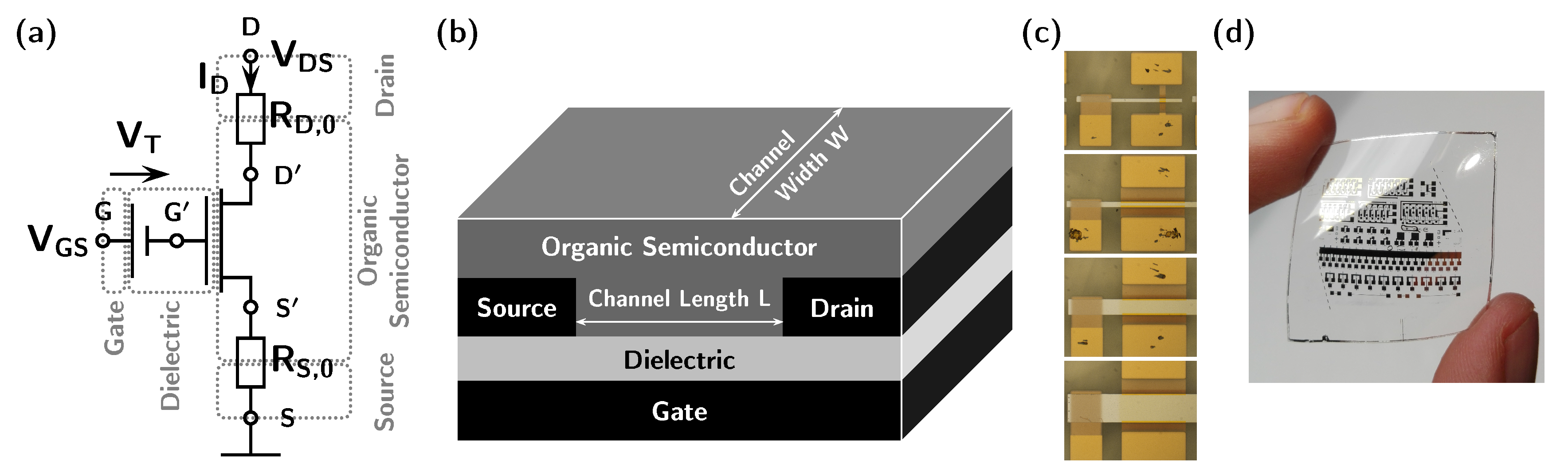
2.1. Equivalent Circuit Model

The equivalent circuit model employed in this work is shown in Figure 1a. This model consists of an ideal field-effect transistor in the gradual channel approximation [23] that is characterized by a charge-carrier mobility that depends on the charge-carrier density [24,25] and on the electric field [7,26] and is terminated by the ideal source S’, drain D’, and gate G’ terminals. At the gate terminal, the threshold voltage V T is implemented as an external bias, and the source and drain terminals are connected to Ohmic contact resistances R S , 0 and R D , 0 . The experimentally-accessible terminals are labeled source S, drain D, and gate G. The assignment of the elements in the equivalent circuit model to the location in a real device is indicated in gray. Figure 1b shows a schematic drawing of a bottom-gate, bottom-contact TFT; Figure 1c shows optical microscopy images of bottom-gate, bottom-contact DNTT TFTs with channel lengths of 2, 8, 40, and 80 μ m from top to bottom; and Figure 1d shows a photograph of a set of pentacene TFTs on a flexible plastic substrate.
The charge-carrier mobility μ at a certain position x in the carrier-accumulation channel is determined by:
μ ( x ) = μ 0 exp β L 0 L V D S V 0 V G S V T V C h S ( x ) V 0 γ
where V C h S ( x ) is the channel potential (with respect to the source) at this position x, V G S = V G S V T is the gate-source voltage, V D S is the drain-source voltage, μ 0 is the mobility prefactor, L is the channel length, β is the exponent of the field sensitivity, γ is the charge-carrier-density sensitivity, L 0 = 1 μ m is a constant length scale, and V 0 is a constant potential scaling factor, with V 0 = 1 V for n-channel (electron-conducting) TFTs and V 0 = 1 V for p-channel (hole-conducting) TFTs. Note that the absolute values of the constant length scale L 0 and the constant potential scale V 0 are chosen arbitrarily and are required only to avoid inconsistencies regarding the units within the corresponding power functions. The exponential term mimics a simplified Poole–Frenkel field dependence [7,26], and the right term describes the charge-carrier-density dependence of the mobility with a power law behavior [24,25].
Incorporating the gradual channel approximation (for details, see [8,23]) leads to an implicit system of equations determining the drain current I D for given applied gate-source voltages and drain-source voltages V G S and V D S :
v G S = 1 V 0 V G S V T I D r S , 0 W v G D = 1 V 0 V G S V T V D S + I D r D , 0 W I D = V 0 | V 0 | W C I μ 0 L ( γ + 2 ) exp β L 0 L v G S v G D v G S γ + 2 Θ ( v G S ) v G D γ + 2 Θ ( v G D )
The reduced voltages v G S and v G D are the voltages between the ideal gate G’, source S’, and drain D’ terminals divided by V 0 . The Heaviside function Θ ( x ) is equal to 1 for x 0 and equal to 0 for x < 0 . C I is the gate capacitance per unit area, and r S , 0 = R S , 0 W and r D , 0 = R D , 0 W are the channel-width-normalized source and drain resistances, respectively. The drain current I D as the output parameter is thus implicitly determined by two input parameters V G S and V D S , six fitting parameters V T , μ 0 , r S , 0 , r D , 0 , β , and γ , two constants L 0 and V 0 , and three geometry parameters L, W, and C I . The gate capacitance per unit area C I is considered here as a geometry parameter since it is determined by the thickness and the permittivity of the gate dielectric.
The implicit system of Equation (2) can be numerically solved with the bisection method, incorporating knowledge of the desired fixed point. We start by setting I D ( 0 ) = 0 A in the first two Equations of (2) to obtain v G S ( 0 ) and v G D ( 0 ) and then substituting the latter in the right-hand side of the third equation. This yields I D ( 1 ) and defines the search interval [ I D , m i n , I D , m a x ] = [ min ( I D ( 0 ) , I D ( 1 ) ) , max ( I D ( 0 ) , I D ( 1 ) ) ] . Now, the recurrent series starts by taking the midpoint I D , M P = ( I D , m i n + I D , m a x ) / 2 and plugging it into the first two equations and the right-hand side of the third equation of (2) to get I D , c a l c . If I D , M P < I D , c a l c , the new search interval is [ I D , M P , min ( I D , m a x , I D , c a l c ) ] , and if I D , M P > I D , c a l c , the new search interval is [ max ( I D , m i n , I D , c a l c ) , I D , M P ] . Calculating I D , M P and I D , c a l c is continued until the desired accuracy is reached.

2.2. Fitting Procedure

The fitting of the measured current-voltage characteristics to this model is accomplished by applying a Gauss–Newton algorithm with the variation of Marquardt [27]. The algorithm is slightly modified here so that it is able to handle minimum and maximum parameter values. In our case, μ 0 , r S , 0 , r D , 0 , and β have to be positive and γ must be greater than 1 . The Gauss–Newton–Marquardt algorithm calculates the difference Δ a = a a ( 0 ) between the previous model parameters a ( 0 ) and the suggested new model parameters a by solving the system of linear equations:
( A + λ D ) Δ a = b
with matrices A and D, the convergence parameter λ introduced by Marquardt, and a vector b . The matrix A is given by:
( A ) i j = k = 1 n 1 σ k 2 I D ( V D S ( k ) , V G S ( k ) ; a ( 0 ) ) a i I D ( V D S ( k ) , V G S ( k ) ; a ( 0 ) ) a j ,
containing the sum over all n measured values k, the standard deviation σ k , and the partial derivatives I D ( V D S ( k ) , V G S ( k ) ; a ( 0 ) ) / a i / j of the calculated drain current I D at the measured data values V D S ( k ) and V G S ( k ) and the previous model parameters a ( 0 ) with respect to the model parameters a i and a j , respectively. The matrix D is a diagonal matrix consisting of the diagonal elements of A, ( D ) i j = δ i j ( A ) i j with δ i j being the Kronecker delta returning 1 if i = j and 0 if i j . The vector b is given by:
b i = k = 1 n I D ( k ) I D ( V D S ( k ) , V G S ( k ) ; a ( 0 ) ) σ k 2 I D ( V D S ( k ) , V G S ( k ) ; a ( 0 ) ) a i
where I D ( k ) is the drain current measured at the drain-source and gate-source voltages V D S ( k ) and V G S ( k ) .
To consider minimum and maximum values of the model parameters, the matrices A and D, the vector b, and the convergence parameter λ are evaluated as in [27], and the system of linear Equation (3) is solved to determine Δ a . Before continuing with this calculated value for Δ a , we need to check whether any of the suggested parameters a = a ( 0 ) + Δ a are out of bounds. For all entries j that are out of bounds, Δ a j is changed so that a j stays within bounds (e.g., Δ a j = a j m a x a j ( 0 ) if the upper boundary is exceeded) and substituted in the system of linear Equation (3) by eliminating the corresponding equation j and transferring ( A ) i j Δ a j to the right-hand side b i b i ( A ) i j Δ a j . The new system of linear equations is solved, and the model parameters are checked again. This procedure is iteratively continued until all model parameters are within bounds. At this point, the Gauss–Newton algorithm is continued.
To calculate the required derivatives of the model function with respect to the model parameters, a few definitions are useful:
T 0 = β L 0 L v G S γ + 2 Θ ( v G S ) v G D γ + 2 Θ ( v G D ) 2 ( γ + 2 ) v G S v G D sgn v G S v G D ,
T G S = v G S γ + 1 Θ ( v G S ) + T 0 ,
T G D = v G D γ + 1 Θ ( v G D ) + T 0 ,
μ ˜ 0 = μ 0 exp β L 0 L v G S v G D ,
D I D = 1 + V 0 C I μ ˜ 0 L T G S r S , 0 + T G D r D , 0
The sign function sgn ( x ) is equal to −1 if x < 0 , equal to 1 if x > 0 , and equal 0 if x = 0 . With these definitions, the derivatives can be written in a compact way as follows:
I D V T = | V 0 | W C I μ ˜ 0 L D I D T G S T G D
I D μ 0 = I D μ 0 D I D
I D r S , 0 = | V 0 | C I μ ˜ 0 T G S I D L D I D
I D r D , 0 = | V 0 | C I μ ˜ 0 T G D I D L D I D
I D γ = I D D I D ( γ + 2 ) V 0 V 0 W C I μ ˜ 0 L ( γ + 2 ) D I D ln ( v G S ) v G S γ + 2 Θ ( v G S ) ln ( v G D ) v G D γ + 2 Θ ( v G D )
I D β = I D D I D L 0 L v G S v G D
In addition to these derivatives, the start values for the fitting procedure are required. Initially, we can set all parameters to zero, except for the mobility prefactor μ 0 and the threshold voltage V T . These two parameters can be estimated from the saturation regime of the output characteristics. In this regime and with only μ 0 and V T being non-zero, the drain current I D is calculated as I D , s a t = W C I μ 0 ( V G S V T ) 2 / 2 L . Performing a linear fit of I D , s a t ( V G S ) provides start values for μ 0 and V T . With these start values, the initial fitting is performed by optimizing only μ 0 and V T . From these optimized parameters, more and more parameters are included in the fitting procedure. The next fit, e.g., is to optimize μ 0 , V T , r S , 0 , and r D , 0 followed by a fit of μ 0 , V T , r S , 0 , r D , 0 , and γ , and a final fit of μ 0 , V T , r S , 0 , r D , 0 , γ , and β . When changing the order of the parameters included in the fitting procedure (e.g., β before γ ), the optimized parameters should converge to the same solution within the chosen numerical accuracy.

2.3. Device Fabrication

All TFTs were fabricated on flexible plastic substrates using aluminum oxide as the gate dielectric. Details regarding the device architecture and the materials employed for the semiconductor and the source and drain contacts, the gate-dielectric thickness and the channel lengths and channel widths can be found in Table 1. The TFTs investigated in detail are bottom-gate, bottom-contact TFTs with a 30 nm-thick layer of DNTT as the semiconductor and Au source and drain contacts functionalized with PFBT to increase the work function of the contacts [28] and to optimize the semiconductor morphology across the contact interface [20]. The 5.3 nm-thick aluminum oxide gate dielectric enables operation voltages below 3 V [29]. This set of TFTs was chosen because the current-voltage characteristics of these TFTs most closely resemble those of an ideal field-effect transistor, as indicated by a nearly perfectly linear relation between the measured drain current and the applied drain-source voltage at small drain-source voltages (i.e., in the linear regime of operation), small contact resistances, and very good device-to-device uniformity. This nearly ideal current-voltage behavior is present even in the TFTs with the smallest channel length implemented here ( L = 2 μ m).
The TFTs of the remaining four sets of devices (i.e., the bottom-gate, top-contact DNTT TFTs [21], the bottom-gate, bottom-contact pentacene TFTs [22], and the bottom-gate, bottom-contact C 60 TFTs [22]) will also be analyzed, albeit only briefly.

3. Results

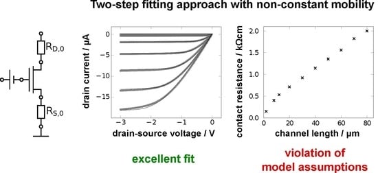
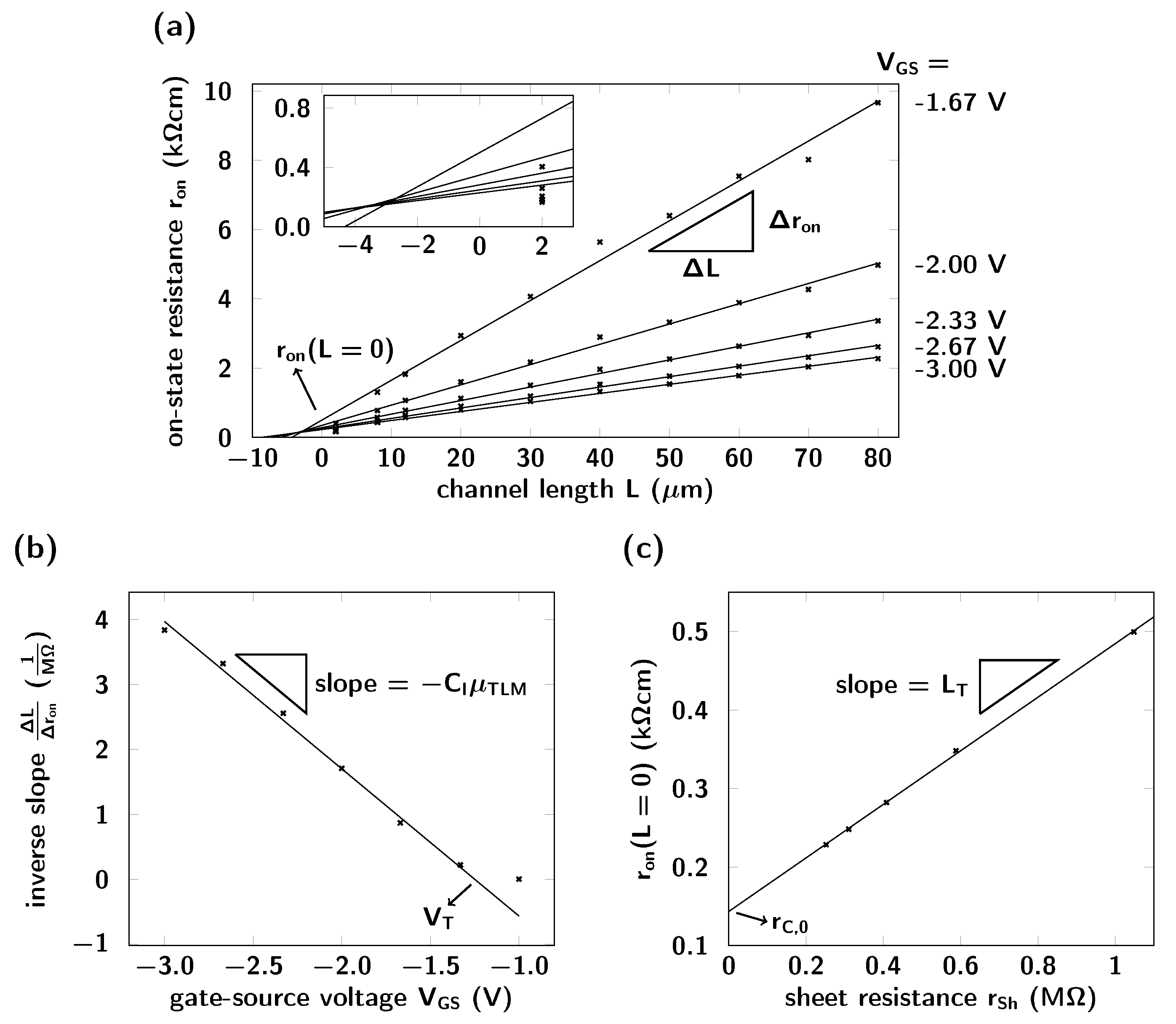
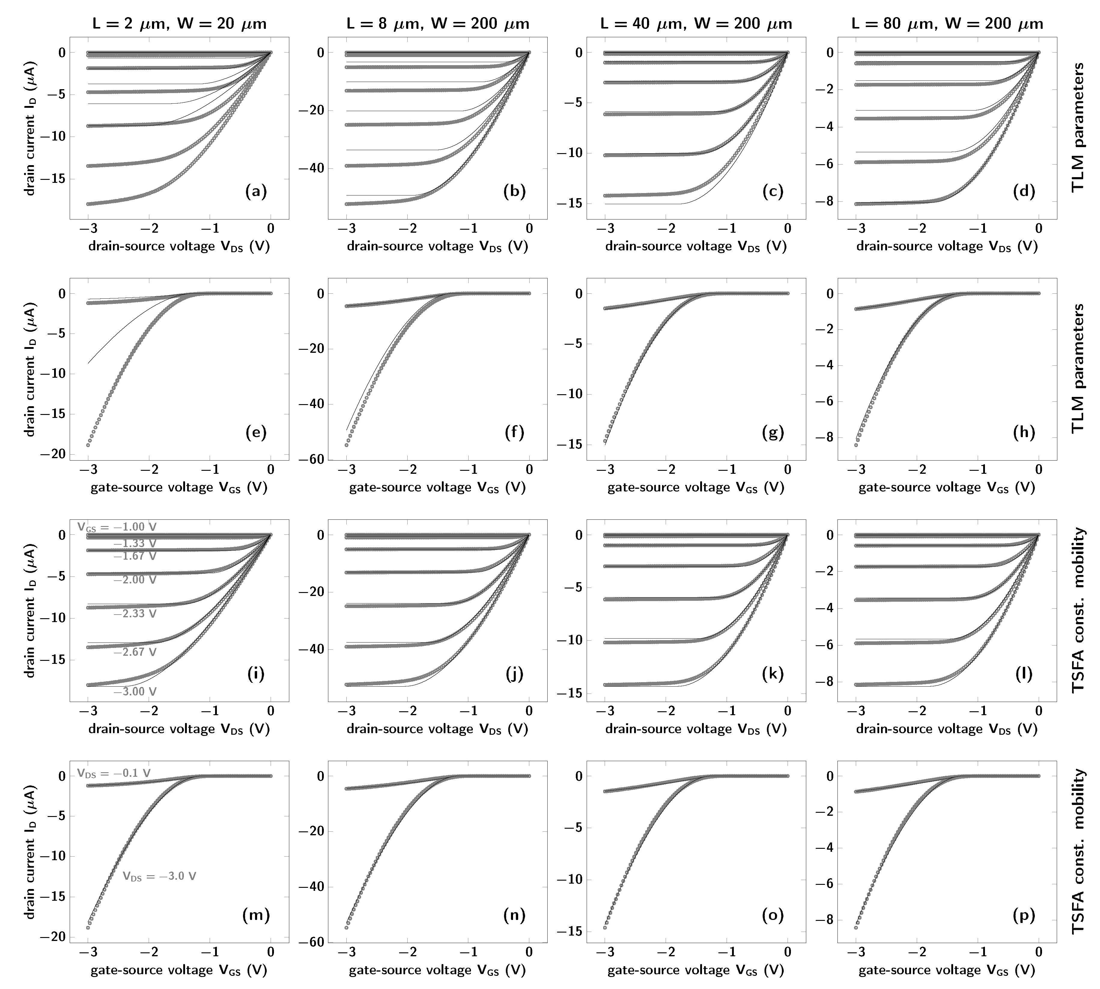
3.1. Conventional Transmission Line Method

Before applying our two-step fitting approach (TSFA), we analyze the data measured on the bottom-contact DNTT TFTs using the popular transmission line method (TLM). This analysis is performed to (i) put the measured current-voltage characteristics into a perspective commonly shared in our field of research and (ii) highlight the benefits and drawbacks of the conventional TLM.
In principle, the TLM can also handle certain non-idealities, such as non-Ohmic contact resistances. However, when applying the most commonly-used extraction procedure proposed in the conventional TLM, the model assumptions are rather strict and require (i) an ideal field-effect transistor in the gradual channel approximation [23] having a charge-carrier mobility that is independent of the electric fields and the charge-carrier density and (ii) Ohmic source and drain resistances [14,15]. Under these model assumptions, the drain current I D in the linear regime of the output characteristics is implicitly determined by:
I D = V 0 W C I μ T L M 2 V 0 L + L T V G S V T I D r S , 0 W 2 V G S V T V D S + I D r D , 0 W 2 .
The transfer length L T accounts for a channel-length-independent extension of the charge-accumulation channel at the contacts. In bottom-gate, top-contact TFTs, L T can be interpreted as an additional distance that the charge carriers travel laterally through the organic semiconductor layer underneath the contacts to reach the charge-accumulation channel (or the drain contact) (see, e.g., [18]). In bottom-gate, bottom-contact TFTs, charges are injected and extracted very close to the channel, so the distances that the carriers travel above the contacts before reaching the channel (or the drain) are very small. This implies that in bottom-gate, bottom-contact TFTs, L T is not necessarily a physically-interpretable parameter, but rather has to be seen as a weighting factor for a non-Ohmic contribution to the contact resistance.
The parameter extraction procedure consists of three parts. In the first part, the on-state resistance r o n is calculated from the slope of the measured output characteristics:
r o n = lim V D S 0 W V D S I D = V 0 L + L T V 0 C I μ T L M V G S V T + r C , 0
with r C , 0 = r S , 0 + r D , 0 . Note that it is important to extract r o n for V D S 0 V because only at this point is it possible to separate the contacts clearly from the channel within the model (cf. Figure S1 in the Supplementary Materials). To determine r o n , we performed a linear fit to the output curves measured for the four smallest drain-source voltages and forced this fit to pass through the origin at V D S = 0 V and I D = 0 A. The plot of the on-state resistance r o n as a function of the channel length L for different gate-source voltages is shown in Figure 2a. As can be seen, the measured on-state resistance is indeed proportional to the channel length, and the linear fits to the measured on-state resistance at different gate-source voltages intersect approximately at L 3.2 μ m and r o n 0.15 k Ω cm.
In the second part of the TLM analysis, the inverse slope Δ L / Δ r o n = C I μ T L M V G S V T V 0 / V 0 is extracted from Figure 2a and plotted as a function of the gate-source voltage V G S (see Figure 2b). The slope of this plot yields the intrinsic channel mobility μ T L M = 3.2 cm 2 /Vs, and the x-axis intersect yields the threshold voltage V T = 1.25 V. In the last part of the TLM analysis, the on-state resistance at a channel length of zero, r o n ( L = 0 ) = r S h L T + r C , 0 , is plotted as a function of the sheet resistance r S h = V 0 [ V 0 C I μ T L M ( V G S V T ) ] 1 (see Figure 2c). The slope of the linear fit to this data is the transfer length L T = 3.4 μ m, and the y-axis intersect yields the Ohmic contact resistance r C , 0 = 0.14 k Ω cm.
The parameters extracted from the conventional TLM analysis can be considered to be reliable only if the following requirements are fulfilled:
  • The measured output characteristics (gray symbols in Figure 3a–d) must be linear for very small drain-source voltages ( V D S 0 V), and the slope of the curves must decrease monotonically as the absolute value of the drain-source voltage V D S increases. An S-shape of the output curves in this regime is an indicator of a non-Ohmic contact resistance.
  • The relations r o n versus L (Figure 2a), Δ L / Δ r o n versus V G S (Figure 2b), and r o n ( L = 0 ) versus r S h (Figure 2c) must be linear.
  • The values for the transfer length L T and the total Ohmic contact resistance r C , 0 obtained from the plot r o n ( L = 0 ) versus r S h (Figure 2c) must be equal to the values for L and r o n at the intersection in Figure 2a.
Figure 2 and Figure 3 confirm that all of these requirements are indeed fulfilled for our set of bottom-gate, bottom-contact DNTT TFTs. Small deviations of the on-state resistances r o n extracted for different channel lengths from the linear fit (see Figure 2a) can be attributed to device-to-device variations. A closer look, however, reveals other, more serious inconsistencies. The inset in Figure 2a shows a close-up of the r o n versus L relation close to L = 0 together with the on-state resistances r o n for the smallest channel length L = 2 μ m (symbols). As can be seen, the linear fits to the r o n versus L data do not intersect in a single point. In addition, all the on-state resistances r o n extracted from the data of the TFT with the smallest channel length ( L = 2 μ m) are a factor of approximately two below the corresponding linear fits. These two inconsistencies do not invalidate a further analysis, because the fact that the linear fits to the r o n versus L data do not intersect in a single point could just be a consequence of the drain-source voltage V D S being too large to be able to extract the on-state resistance r o n in a reliable manner (cf. Figure S1), and the deviation of the on-state resistances r o n extracted from the data of the TFT with the channel length of L = 2 μ m might be caused by short-channel effects. These explanations do not necessarily compromise the validity of the model system.
As we are able to calculate the electrical TFT characteristics for a given set of device parameters, we can now compare the output and transfer characteristics calculated using the parameters extracted from the TLM analysis to the measured output and transfer characteristics. This comparison is shown in Figure 3a–h for TFTs with channel lengths of 2, 8, 40, and 80 μ m. As can be seen, the calculated output curves (black lines) deviate substantially from the measured output curves (gray symbols), regardless of the channel length. These deviations indicate a problem within the transistor model underlying the TLM that had evaded the reliability check performed above. Upon closer inspection, it can be noticed that the agreement between the calculated and measured output and transfer curves is particularly poor when the channel length is small (Figure 3a,e). For the three larger channel lengths (8, 40, and 80 μ m; Figure 3b–d), the slope of the output curves at small drain-source voltages (linear regime) is captured reasonably well, but the agreement becomes increasingly worse with increasing absolute value of the drain-source voltage (saturation regime). The better agreement between the calculated and the measured output curves at small drain-source voltages (linear regime) is due to the fact that the transistor parameters in the TLM analysis were extracted for V D S 0 V.

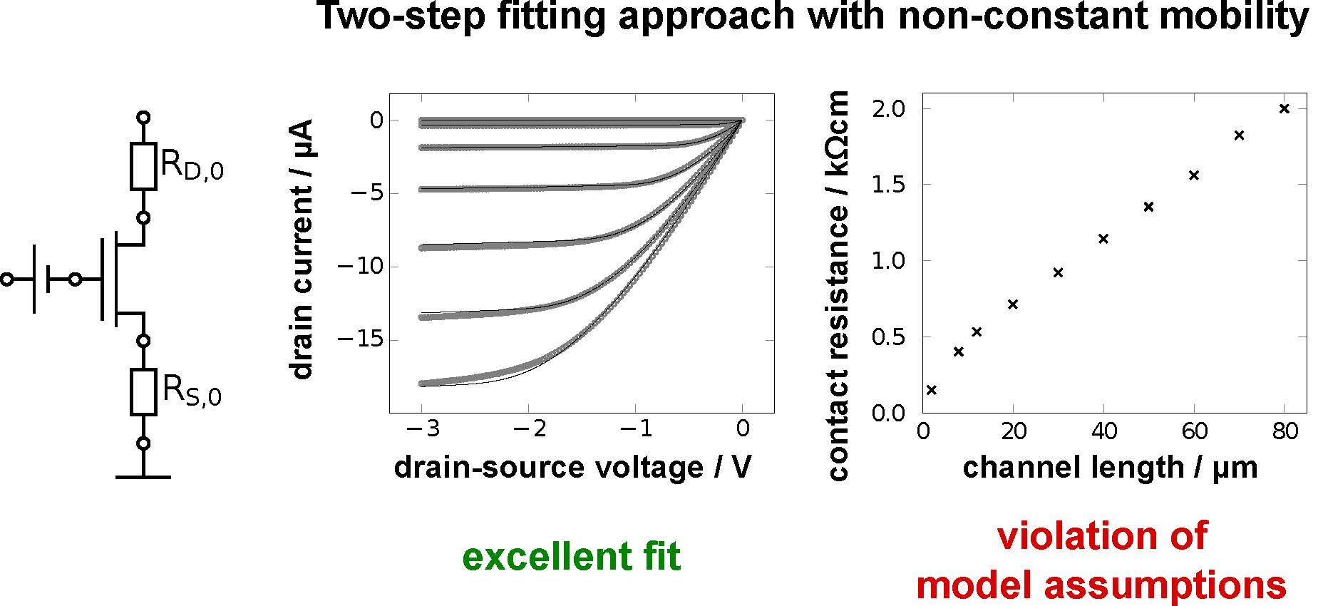
3.2. TSFA with Constant-Mobility Model

The conventional TLM analysis is able to produce reliable results only if all model parameters are identical for all transistors within the set of devices with different channel lengths. This is a substantial weakness of the conventional TLM, because in reality, these parameters can vary considerably, even for nominally identical organic transistors. Such device-to-device variations may explain the deviations between the calculated and the measured output and transfer characteristics, as seen in Figure 3a–h. Therefore, the question arises whether these deviations can be attributed to the extraction method (TLM) or to the underlying transistor model. To answer this question, we have analyzed the measured TFT data using our TSFA. We have extracted a charge-carrier mobility μ T S F A , a threshold voltage V T , and source and drain resistances r S , 0 and r D , 0 for each TFT individually. Note that the transfer length L T cannot be evaluated in the first step of the TSFA, and the charge-carrier mobility extracted within the TSFA is related to the intrinsic channel mobility μ T L M extracted using the TLM as μ T S F A / L = μ T L M / ( L + L T ) . The output and transfer characteristics calculated with this approach are shown in Figure 3i–p. For all channel lengths, the agreement between the output and transfer curves calculated using our TSFA and the measured output and transfer curves (Figure 3i–p) is significantly better than the agreement between the output and transfer curves calculated using the parameters obtained from the conventional TLM analysis and the measured output and transfer curves (Figure 3a–h). The deviations between the calculated and the measured output characteristics seen in Figure 3i–l are discussed in detail below. Since these deviations are relatively small and the deviations in the transfer curves (Figure 3m–p) are even smaller, the main message taken from Figure 3i–p is that the first step of our TSFA is conditionally passed.
For the second step of our TSFA, we plot the extracted transistor parameters as a function of the channel length, as shown in Figure 4. To be consistent with the model assumptions, these parameters would have to be independent of the channel length L. Figure 4 shows that this is clearly not the case. In Figure 4a, it can be seen that the absolute value of the threshold voltage V T decreases by about 100 mV as the channel length is decreased from 40 μ m–2 μ m. This is the well-known threshold-voltage roll-off that occurs in all field-effect transistors (cf. [30], Chapter 6.4.2). Figure 4b shows a pronounced dependence of the charge-carrier mobility μ T S F A on the channel length L (symbols). If we were to strictly stick to the model underlying the TLM, we could surmise that this dependence might be related to the transfer length L T . To check whether the introduction of a transfer length conceptually lifts the observed channel-length dependence, we can incorporate L T into the second step of the TSFA by replacing the mobility μ T S F A with the term μ T L M L L + L T , where μ T L M should be independent of the channel length. This relation is reminiscent of, but not equivalent to the relation between effective mobility and intrinsic channel mobility (cf. [21,31]). A fit to the relation μ T S F A = μ T L M L L + L T is shown as a solid line in Figure 4b. As can be seen, the agreement between the fit and the data is quite poor, as the fit systematically overestimates the extracted parameters for intermediate channel lengths ( 8 L 40 μ m) and underestimates them for large channel lengths ( L 50 μ m). This poor agreement indicates a problem with the model system. Figure 4c displays the combined contact resistance r C , 0 = r S , 0 + r D , 0 . Rather than being independent of the channel length, the contact resistance r C , 0 increases by more than a factor of three with increasing channel length, which is a clear indicator of an inadequate transistor model.
An explanation for the failure of the constant-mobility model can be found by taking a closer look at the deviations between the calculated and the measured output characteristics in Figure 3i–l. We notice that neither the transition between the linear regime and the saturation regime, nor the saturation of the drain current at large drain-source voltages in the measured output curves are properly reproduced in the calculated output curves. The first of these symptoms occurs regardless of the channel length and can be alleviated by assuming that the charge-carrier mobility is a function of the charge-carrier density of the form μ = μ 0 ( V G V C h ) γ , as suggested by the percolation theory [24] or by the multiple trapping and release model [25]. The second symptom is more pronounced for shorter channels, which indicates a field-dependence of the charge-carrier mobility. As a first attempt, we assume a simplified Poole–Frenkel behavior of the form exp ( β V D S / L ) [7,26].

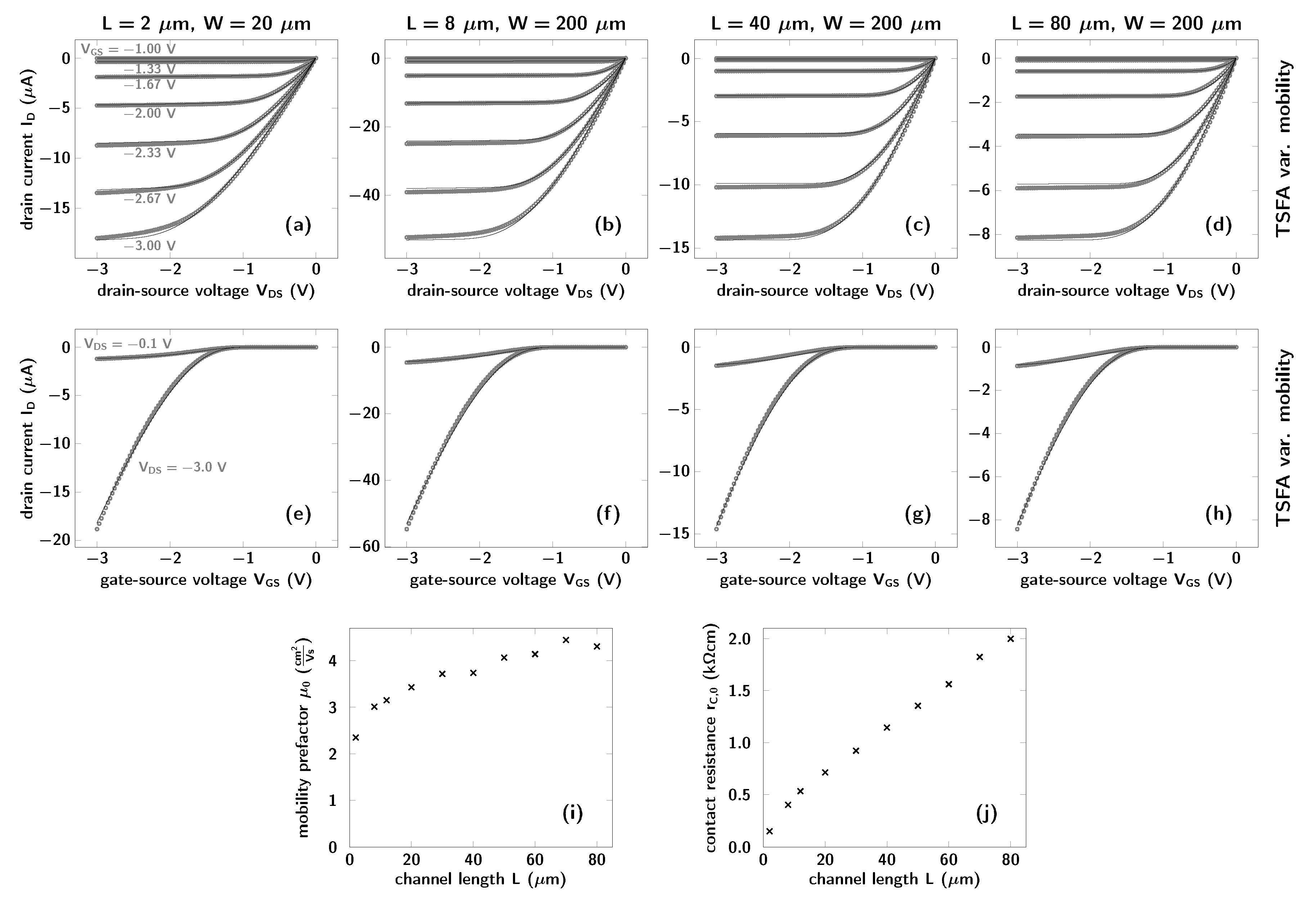
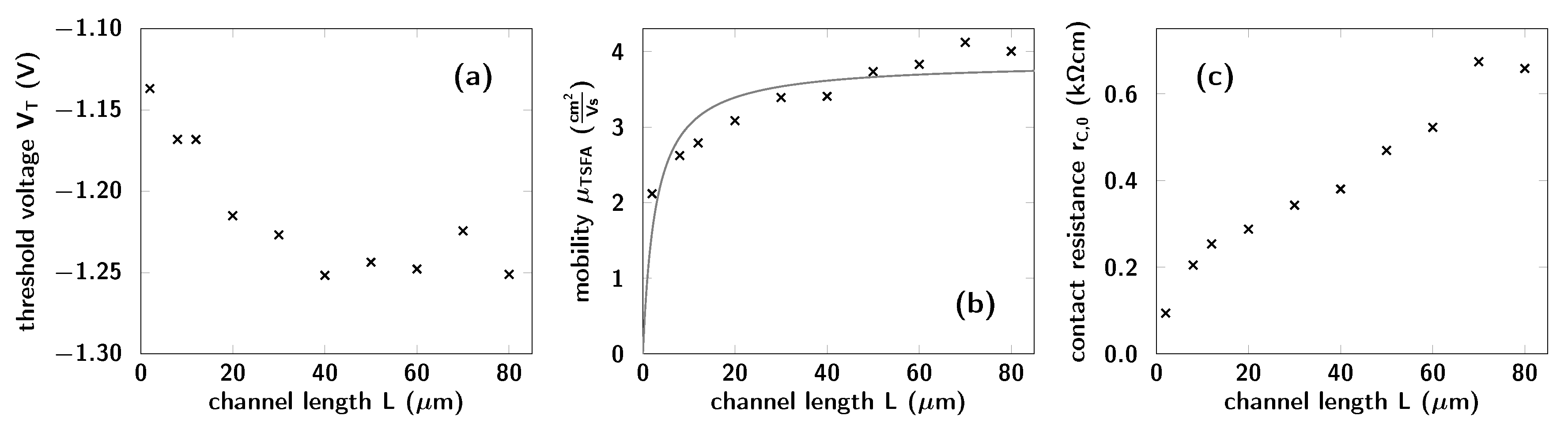
3.3. TSFA with Field- and Charge-Carrier-Density-Dependent Mobility

Incorporating a field- and charge-carrier-density-dependent mobility in the model leads to a significantly better agreement between the calculated and the measured output and transfer characteristics (Figure 5a–h) compared to the constant-mobility model (cf. Figure 3i–p). Especially for the TFT with the smallest channel length (Figure 3i,m and Figure 5a,e), the agreement is substantially improved due to the fact that the Poole–Frenkel model provides a far more realistic description of the saturation regime. For all channel lengths, the agreement between the calculated and the measured output curves (Figure 5a–d) is nearly perfect for the smaller gate-source voltages ( V G S < 2.5 V). For the transfer curves (Figure 5e–h), a slight improvement at the branching point at a gate-source voltage of about V G S = 1.5 V can be seen compared to the constant-mobility model (Figure 3m–p). We again move on to examine the channel-length dependence of the extracted parameters. The most relevant parameters are the mobility prefactor μ 0 and the combined contact resistance r C , 0 = r S , 0 + r D , 0 shown in Figure 5i,j. The mobility prefactor μ 0 exhibits a slightly smaller channel-length dependence compared to the charge-carrier mobility μ T S F A examined earlier (cf. Figure 4b). The channel-length dependence of r C , 0 is even more pronounced, with a ratio of approximately one order of magnitude between that of the TFT with the largest channel length and that of the TFT with the smallest channel length (see Figure 5j), causing this model to fail. To illustrate the significant influence of the channel-length-dependence of the contact resistance, Figure S2 shows the disagreement between the calculated and the measured output characteristics when considering the contact resistances of the TFTs with the smallest channel length (Figure S2a–d) and of the TFTs with the largest channel length (Figure S2e–h). The remaining parameters, V T , γ , and β do not have such a pronounced channel-length dependence (not shown).
To identify the problem of the model, we again inspect the calculated and the measured output characteristics (Figure 5a–d). For all channel lengths, the output curves calculated for V G S = 2.67 V lie above and the output curves calculated for V G S = 3.00 V lie below the measured output curves. This inaccurate spacing of the curves in the saturation regime is an indicator for a problem of the charge-carrier-density dependence of the charge-carrier mobility, which is predominantly determined by the gate-source voltage V G S . The spacing of the curves in the saturation regime is determined not only by the charge-carrier-density dependence of the mobility, but also by the contact resistances (explained in more detail in Figure S3). Assuming a constant mobility and zero contact resistance, the saturation current I D , s a t increases quadratically with the gate-source voltage, ( V G S V T ) 2 . On the other hand, assuming a constant mobility and a very large contact resistance, the saturation current would increase linearly with increasing gate-source voltage. This means that increasing both the mobility and the contact resistance can lead to similar output curves for the largest gate-source voltage and different spacings for smaller gate-source voltages (see Figure S3).
This effect may explain the increase of r C , 0 with L in the following way: If the charge-carrier- density dependence of the charge-carrier mobility is captured incorrectly, the spacing of the output characteristics for different gate-source voltages will be inaccurate, as well. The incorrect spacing can be compensated by a correspondingly incorrect choice of the contact resistances. As the error in the mobility scales with the channel length in the calculation of the drain current because it is a channel property and the influence of the contact resistance on the drain current is not affected by the channel length, the value extracted for the contact resistance is forced to scale with L in order to compensate the incorrect mobility.
The over- and under-estimation of the drain current for the second-most-negative and the most-negative gate-source voltage suggests that the contact resistance decreases the spacing for more-negative gate-source voltages and, hence, is too large. This change in spacing can alternatively be achieved if the mobility would decrease with increasing charge-carrier density. This decrease should occur only for large charge-carrier densities, because for small charge-carrier densities, i.e., at small gate-source voltages, the increasing mobility in the improved TFT model describes the measured output curves substantially better than the constant-mobility model. Thus, the evaluation of our TSFA suggests that the mobility should first increase and then decrease as the charge-carrier density is increased. Indications for such a behavior of the mobility were recently found experimentally by Bittle et al. [32] and Uemura et al. [33]; Fishchuk et al. [34] suggested such a behavior from a theoretical point of view.
Besides improving the mobility, another possible problem with the transistor model is that the gradual channel approximation does not take into account that organic semiconductors are in principle electrical insulators and that all mobile charges have to be provided by the metal contacts. Unlike in field-effect transistors based on doped semiconductors, such as silicon MOSFETs, these mobile charges in organic semiconductors are not compensated in the semiconductor by charges of opposite polarity. This uncompensated charge accumulation affects the electric field at the source and drain contacts, and this effect becomes more pronounced with increasing channel length. Including this charge cloud in the transistor model might also help alleviate the channel-length dependence of the contact resistance.

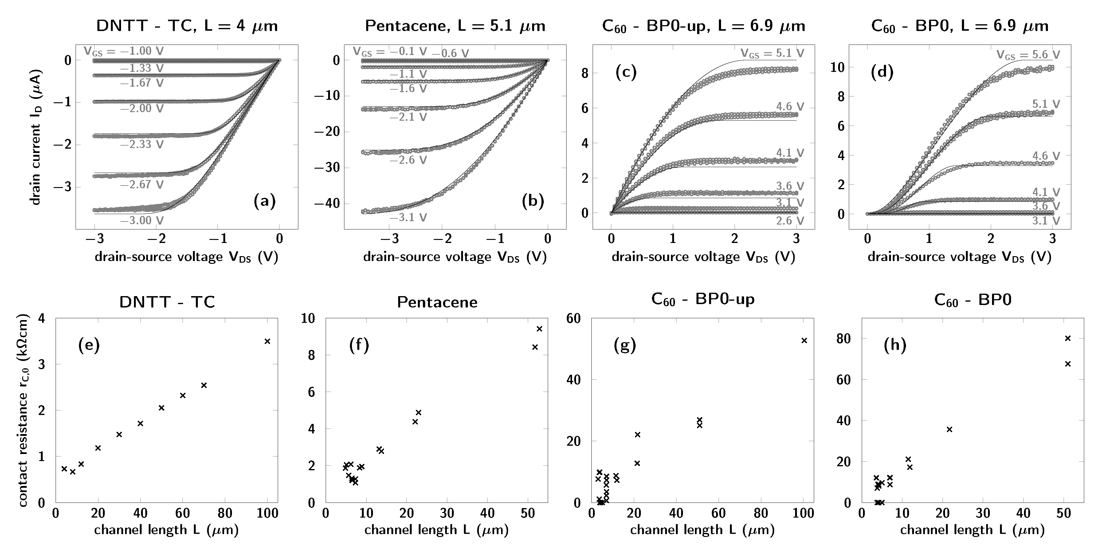
3.4. Testing Other Organic-TFT Technologies

We note that the failure of the transistor model discussed above is not exclusive to the bottom-gate, bottom-contact DNTT TFTs investigated above, as the model has also failed for the bottom-gate, top-contact DNTT TFTs [21] and the bottom-gate, bottom-contact pentacene and C 60 TFTs [22]. For the bottom-gate, top-contact DNTT TFTs and the bottom-gate, bottom-contact C 60 TFTs, we were able to obtain acceptable agreement between the calculated and the measured current-voltage characteristics by modeling the non-linearity in the linear regime of the output characteristics using a gate-voltage-dependent Schottky diode at the source contact [22]. Selected examples of calculated and measured output characteristics for each set of TFTs are shown in Figure 6a–d. The deviations between the calculated output characteristics and the measured output characteristics are similar to those for the bottom-gate, bottom-contact DNTT TFTs, exhibiting an overestimation of the absolute value of the drain current for the largest absolute value of the gate-source voltage and an underestimation for the smaller ones.
Figure 6e–h shows the Ohmic component of the combined contact resistance r C , 0 as a function of the channel length L for the bottom-gate, top-contact DNTT TFTs (Figure 6e), the bottom-gate, bottom-contact pentacene TFTs with Au contacts functionalized with 2-phenylpyrimidine-5-thiol (BP0-down) (Figure 6f), and the bottom-gate, bottom-contact C 60 TFTs with Au contacts functionalized with either 4-(2-mercaptophenyl)pyrimidine (BP0-up) or biphenyl-4-thiol (BP0) (Figure 6g,h). The approximately linear dependence of r C , 0 on the channel length causes a similar failure of the transistor model during the second step of our TSFA for each set of TFTs.

4. Summary and Conclusions

We have proposed a two-step fitting approach (TSFA) to check whether or not a transistor model is capable of describing the experimentally-obtained current-voltage characteristic of organic TFTs. Only a valid transistor model that correctly discriminates between contact and channel properties enables the user to reliably extract, interpret, and compare contact resistances and charge-carrier mobilities of organic TFTs. Our TSFA relies on a series of transistors with different channel lengths and consists of two steps. First, the chosen transistor model is fitted to all data points of the measured output and transfer characteristics of each TFT individually in order to extract the transistor parameters of each device. Second, it is determined whether or not the extracted parameters depend on the channel length. This consistency check is successful if (i) the measured current-voltage curves are represented well by the current-voltage curves calculated using the model and the extracted transistor parameters and if (ii) the extracted parameters are independent of the channel length. Our approach offers a clear benefit compared to conventional parameter-extraction methods in that the reliability of the underlying transistor model can be easily validated. Due to the analysis of each individual TFT as a whole, the reason for a failure of the transistor model can be identified based on the nature of the deviations between the calculated and the measured current-voltage characteristics.
We have outlined the indicators that are available to judge the consistency within the TSFA by using the transistor model underlying the conventional transmission line method (TLM) as an illustrative example. Organic TFTs with particularly small contact resistances whose operation resembles the ideal transistor behavior most closely were analyzed in particular detail. With this set of TFTs, we have demonstrated that not all types of inconsistencies can be spotted within the parameter-extraction step, but rather require a second step for validity checking. A conventional TLM analysis of this set of TFTs initially gave an apparently consistent picture comprising (i) a linear onset of the output characteristics for zero drain-source voltage and (ii) a good agreement of all calculated linear fits. However, the output characteristics calculated using the extracted parameters failed to reproduce the measured output characteristics. The subsequent validity check of the TSFA for the model underlying the TLM was not passed, because the extracted contact resistances retained a pronounced dependence on the channel length. Such inconsistencies ought to be removed or at least alleviated by improving the underlying transistor model. For example, the model underlying the TLM can be improved by accounting for a field- and charge-carrier-density-dependent mobility [7,24,25,26]. Even though the TSFA leads to better agreement between the calculated and the measured output characteristics, the improved model still fails the subsequent validity check of the TSFA, due to a remnant channel-length dependence of the contact resistance. The failure of the advanced transistor model featuring a field- and charge-carrier-density-dependent mobility has been demonstrated for a wide variety of organic TFTs based on different device architectures, different organic semiconductors, and source and drain contacts with poor injection behavior that caused profound non-linear contributions to the contact resistance.
To improve the currently-available transistor models, we need to face two aspects: On the one hand, the analysis of the deviations between the calculated and the measured current-voltage characteristics suggests that the charge-carrier-density dependence of the charge-carrier mobility is not properly captured. Hence, a mobility model that is particularly suitable for the predominantly two-dimensional charge transport through the charge-accumulation channel of a TFT needs to be developed. On the other hand, the gradual channel approximation should be reconsidered by accounting for the charge accumulation in the channel. Due to the lack of compensation by charges of opposite polarity within the organic semiconducting layer, this uncompensated charge accumulation affects the electric-field distribution, causing notable changes at the contacts. These changes become more important for larger channel lengths. Our TSFA can be used to check each stage of model improvement.

Supplementary Materials

The following are available online at https://www.mdpi.com/2073-4352/9/2/85/s1.

Author Contributions

Data analysis and writing, original draft preparation, M.K. and K.Z.; fabrication and measurement of DNTT TFTs, J.W.B. and H.K.; fabrication and measurement of pentacene and C 60 TFTs, A.P., E.K.-P., G.S., and B.S.; editing J.W.B., H.K., M.K., and K.Z.

Funding

This research was funded by FWF Grant Number I 2081-N20.

Conflicts of Interest

The authors declare no conflict of interest.

References

  1. Guo, X.; Xu, Y.; Ogier, S.; Ng, T.N.; Caironi, M.; Perinot, A.; Li, L.; Zhao, J.; Tang, W.; Sporea, R.A.; et al. Current Status and Opportunities of Organic Thin-Film Transistor Technologies. IEEE Trans. Electron Devices 2017, 64, 1906–1921. [Google Scholar] [CrossRef]
  2. Paterson, A.F.; Singh, S.; Fallon, K.J.; Hodsden, T.; Han, Y.; Schroeder, B.C.; Bronstein, H.; Heeney, M.; McCulloch, I.; Anthopoulos, T.D. Recent Progress in High-Mobility Organic Transistors: A Reality Check. Adv. Mater. 2018, 30, 1801079. [Google Scholar] [CrossRef] [PubMed]
  3. Yamamura, A.; Watanabe, S.; Uno, M.; Mitani, M.; Mitsui, C.; Tsurumi, J.; Isahaya, N.; Kanaoka, Y.; Okamoto, T.; Takeya, J. Wafer-scale, layer-controlled organic single crystals for high-speed circuit operation. Sci. Adv. 2018, 4, eaao5758. [Google Scholar] [CrossRef] [PubMed]
  4. Ogier, S.D.; Matsui, H.; Feng, L.; Simms, M.; Mashayekhi, M.; Carrabina, J.; Terés, L.; Tokito, S. Uniform, high performance, solution processed organic thin-film transistors integrated in 1 MHz frequency ring oscillators. Org. Electron. 2018, 54, 40–47. [Google Scholar] [CrossRef]
  5. Pasveer, W.F.; Cottaar, J.; Tanase, C.; Coehoorn, R.; Bobbert, P.A.; Blom, P.W.M.; de Leeuw, D.M.; Michels, M.A.J. Unified Description of Charge-Carrier Mobilities in Disordered Semiconducting Polymers. Phys. Rev. Lett. 2005, 94. [Google Scholar] [CrossRef] [PubMed]
  6. Li, J.; Ou-Yang, W.; Weis, M. Electric-field enhanced thermionic emission model for carrier injection mechanism of organic field-effect transistors: Understanding of contact resistance. J. Phys. D Appl. Phys. 2017, 50, 035101. [Google Scholar] [CrossRef]
  7. Locci, S.; Morana, M.; Orgiu, E.; Bonfiglio, A.; Lugli, P. Modeling of Short-Channel Effects in Organic Thin-Film Transistors. IEEE Trans. Electron Devices 2008, 55, 2561–2567. [Google Scholar] [CrossRef]
  8. Marinov, O.; Deen, M.J.; Zschieschang, U.; Klauk, H. Organic Thin-Film Transistors: Part I—Compact DC Modeling. IEEE Trans. Electron Devices 2009, 56, 2952–2961. [Google Scholar] [CrossRef]
  9. Di Pietro, R.; Venkateshvaran, D.; Klug, A.; List-Kratochvil, E.J.W.; Facchetti, A.; Sirringhaus, H.; Neher, D. Simultaneous extraction of charge density dependent mobility and variable contact resistance from thin film transistors. Appl. Phys. Lett. 2014, 104, 193501. [Google Scholar] [CrossRef]
  10. Natali, D.; Caironi, M. Charge injection in solution-processed organic field-effect transistors: Physics, models and characterization methods. Adv. Mater. 2012, 24, 1357–1387. [Google Scholar] [CrossRef]
  11. Wang, S.D.; Yan, Y.; Tsukagoshi, K. Transition-Voltage Method for Estimating Contact Resistance in Organic Thin-Film Transistors. IEEE Electron Device Lett. 2010, 31, 509–511. [Google Scholar] [CrossRef]
  12. Takagaki, S.; Yamada, H.; Noda, K. Extraction of contact resistance and channel parameters from the electrical characteristics of a single bottom-gate/top-contact organic transistor. Jpn. J. Appl. Phys. 2016, 55, 03DC07. [Google Scholar] [CrossRef]
  13. Torricelli, F.; Ghittorelli, M.; Colalongo, L.; Kovacs-Vajna, Z.M. Single-transistor method for the extraction of the contact and channel resistances in organic field-effect transistors. Appl. Phys. Lett. 2014, 104, 093303. [Google Scholar] [CrossRef]
  14. Kanicki, J.; Libsch, F.R.; Griffith, J.; Polastre, R. Performance of thin hydrogenated amorphous silicon thin-film transistors. J. Appl. Phys. 1991, 69, 2339–2345. [Google Scholar] [CrossRef]
  15. Luan, S.; Neudeck, G.W. An experimental study of the source/drain parasitic resistance effects in amorphous silicon thin film transistors. J. Appl. Phys. 1992, 72, 766–772. [Google Scholar] [CrossRef]
  16. Natali, D.; Fumagalli, L.; Sampietro, M. Modeling of organic thin film transistors: Effect of contact resistances. J. Appl. Phys. 2007, 101, 014501. [Google Scholar] [CrossRef]
  17. Deen, M.J.; Marinov, O.; Zschieschang, U.; Klauk, H. Organic Thin-Film Transistors: Part II—Parameter Extraction. IEEE Trans. Electron Devices 2009, 56, 2962–2968. [Google Scholar] [CrossRef]
  18. Fischer, A.; Zündorf, H.; Kaschura, F.; Widmer, J.; Leo, K.; Kraft, U.; Klauk, H. Nonlinear Contact Effects in Staggered Thin-Film Transistors. Phys. Rev. Appl. 2017, 8, 054012. [Google Scholar] [CrossRef]
  19. Mayer, J.; Khairy, K.; Howard, J. Drawing an elephant with four complex parameters. Am. J. Phys. 2010, 78, 648–649. [Google Scholar] [CrossRef]
  20. Gundlach, D.J.; Royer, J.E.; Park, S.K.; Subramanian, S.; Jurchescu, O.D.; Hamadani, B.H.; Moad, A.J.; Kline, R.J.; Teague, L.C.; Kirillov, O.; et al. Contact-induced crystallinity for high-performance soluble acene-based transistors and circuits. Nat. Mater. 2008, 7, 216–221. [Google Scholar] [CrossRef]
  21. Kraft, U.; Takimiya, K.; Kang, M.J.; Rödel, R.; Letzkus, F.; Burghartz, J.N.; Weber, E.; Klauk, H. Detailed analysis and contact properties of low-voltage organic thin-film transistors based on dinaphtho[2,3- b:2’,3’f]thieno[3,2-b]thiophene (DNTT) and its didecyl and diphenyl derivatives. Org. Electron. 2016, 35, 33–40. [Google Scholar] [CrossRef]
  22. Petritz, A.; Krammer, M.; Sauter, E.; Gärtner, M.; Nascimbeni, G.; Schrode, B.; Fian, A.; Gold, H.; Cojocaru, A.; Karner-Petritz, E.; et al. Embedded Dipole Self-Assembled Monolayers for Contact Resistance Tuning in p-Type and n-Type Organic Thin Film Transistors and Flexible Electronic Circuits. Adv. Funct. Mater. 2018, 28, 1804462. [Google Scholar] [CrossRef]
  23. Shockley, W. A Unipolar “Field-Effect” Transistor. Proc. IRE 1952, 40, 1365–1376. [Google Scholar] [CrossRef]
  24. Vissenberg, M.C.J.M.; Matters, M. Theory of the field-effect mobility in amorphous organic transistors. Phys. Rev. B 1998, 57, 12964–12967. [Google Scholar] [CrossRef]
  25. Horowitz, G.; Hajlaoui, M.E.; Hajlaoui, R. Temperature and gate voltage dependence of hole mobility in polycrystalline oligothiophene thin film transistors. J. Appl. Phys. 2000, 87, 4456–4463. [Google Scholar] [CrossRef]
  26. Hall, R.B. The Poole-Frenkel effect. Thin Solid Films 1971, 8, 263–271. [Google Scholar] [CrossRef]
  27. Marquardt, D. An Algorithm for Least-Squares Estimation of Nonlinear Parameters. J. Soc. Ind. Appl. Math. 1963, 11, 431–441. [Google Scholar] [CrossRef]
  28. Hong, J.P.; Park, A.Y.; Lee, S.; Kang, J.; Shin, N.; Yoon, D.Y. Tuning of Ag work functions by self-assembled monolayers of aromatic thiols for an efficient hole injection for solution processed triisopropylsilylethynyl pentacene organic thin film transistors. Appl. Phys. Lett. 2008, 92, 143311. [Google Scholar] [CrossRef]
  29. Borchert, J.W.; Peng, B.; Letzkus, F.; Burghartz, J.N.; Chan, P.K.L.; Zojer, K.; Ludwigs, S.; Klauk, H. Small contact resistance and high-frequency operation of flexible, low-voltage, inverted coplanar organic transistors. Nat. Commun. 2019, submitted. [Google Scholar]
  30. Sze, S.M.; Ng, K.K. Physics of Semiconductor Devices; OCLC: 488586029; John Wiley & Sons: New York, NY, USA, 2007. [Google Scholar]
  31. Rödel, R.; Letzkus, F.; Zaki, T.; Burghartz, J.N.; Kraft, U.; Zschieschang, U.; Kern, K.; Klauk, H. Contact properties of high-mobility, air-stable, low-voltage organic n-channel thin-film transistors based on a naphthalene tetracarboxylic diimide. Appl. Phys. Lett. 2013, 102, 233303. [Google Scholar] [CrossRef]
  32. Bittle, E.G.; Basham, J.I.; Jackson, T.N.; Jurchescu, O.D.; Gundlach, D.J. Mobility overestimation due to gated contacts in organic field-effect transistors. Nat. Commun. 2016, 7, 10908. [Google Scholar] [CrossRef] [PubMed]
  33. Uemura, T.; Rolin, C.; Ke, T.H.; Fesenko, P.; Genoe, J.; Heremans, P.; Takeya, J. On the Extraction of Charge Carrier Mobility in High-Mobility Organic Transistors. Adv. Mater. 2016, 28, 151–155. [Google Scholar] [CrossRef] [PubMed]
  34. Fishchuk, I.I.; Arkhipov, V.I.; Kadashchuk, A.; Heremans, P.; Bässler, H. Analytic model of hopping mobility at large charge carrier concentrations in disordered organic semiconductors: Polarons versus bare charge carriers. Phys. Rev. B 2007, 76, 045210. [Google Scholar] [CrossRef]
Figure 1. Panel (a) shows the equivalent circuit model based on an ideal field-effect transistor in the gradual channel approximation with a field- and charge-carrier-density-dependent mobility connected to the Ohmic source and drain resistances R S , 0 and R D , 0 . The threshold voltage V T is implemented in the form of an external bias. The terminals of the ideal transistor are labeled source S’, drain D’, and gate G’, and the experimentally-accessible terminals are labeled source S, drain D, and gate G. The corresponding location of the elements in a real device is indicated in gray. In (b), a schematic drawing of a bottom-gate, bottom-contact thin-film transistor (TFT) is illustrated. In (c), optical microscopy images of bottom-gate, bottom-contact dinaphtho[2,3-b:2’,3’-f]thieno[3,2-b]thiophene (DNTT) TFTs with channel lengths of 2, 8, 40, and 80 μ m from top to bottom can be seen, and (d) shows a photograph of a set of pentacene TFTs on a flexible plastic substrate.
Crystals 09 00085 g001
Figure 2. Parameter extraction in the framework of the conventional transmission line method (TLM), performed here on a set of bottom-gate, bottom-contact p-channel TFTs based on the small-molecule semiconductor DNTT. In (a), the on-state resistance r o n = W V D S / I D for V D S 0 V, extracted from the measured output characteristics, is plotted as a function of the channel length for different gate-source voltages V G S . From a linear fit to the data, the inverse slope Δ L / Δ r o n and the y-axis intersect r o n ( L = 0 ) are extracted. The inset shows a magnification of the region in which the linear fits intersect and the extracted r o n values for the smallest channel length of L = 2 μ m (symbols). In (b), Δ L / Δ r o n is plotted as a function of the gate-source voltage V G S , and from the linear fit to the data, the threshold voltage V T = 1.25 V and the intrinsic channel mobility μ T L M = 3.2 cm 2 /Vs are obtained. In (c), r o n ( L = 0 ) = r S h L T + r C , 0 is plotted as a function of the sheet resistance r S h = V 0 [ V 0 C I μ T L M ( V G S V T ) ] 1 , and from the linear fit to the data, the transfer length L T = 3.4 μ m and the total Ohmic contact resistance r C , 0 = 0.14 k Ω cm are obtained.
Crystals 09 00085 g002
Figure 3. Measured output and transfer characteristics (gray symbols) and calculated output and transfer characteristics (black lines) of bottom-gate, bottom-contact DNTT TFTs with channel lengths L of 2, 8, 40, and 80 μ m. The TFT with a channel length of 2 μ m has a channel width of 20 μ m, while the TFTs with channel lengths of 8, 40, and 80 μ m have a channel width of 200 μ m. Note that the gray symbols appear as an apparent thick line due to the close spacing of the data points. In (ah), the output and transfer curves were calculated using the transistor parameters extracted using the conventional TLM analysis. In (ip), the output and transfer curves were calculated using our two-step fitting approach (TSFA) with the constant-mobility model underlying the conventional TLM.
Crystals 09 00085 g003
Figure 4. Dependence of the transistor parameters extracted using the TSFA for the theoretical transistor model underlying the conventional TLM on the channel length L. In (a), it can be seen that the threshold voltage V T shows only a very small dependence on the channel length. Panel (b) indicates that the dependence of the charge-carrier mobility μ T S F A on the channel length L (symbols) is not properly described by the equation μ T S F A = μ T L M L / ( L + L T ) (solid line), with L T being the transfer length. In (c), the distinct linear increase of the contact resistance r C , 0 = r S , 0 + r D , 0 with increasing channel length L cannot be explained at all. As a consequence, the model does not pass the second step.
Crystals 09 00085 g004
Figure 5. Results of the TSFA for the model with a field- and charge-carrier-density-dependent mobility. In (ah), the measured output and transfer characteristics (gray symbols) and the calculated output and transfer characteristics (black lines) of bottom-gate, bottom-contact DNTT TFTs with channel lengths L of 2, 8, 40, and 80 μ m and channel widths W of 20 or 200 μ m are shown, indicating good agreement. Note that the gray symbols appear as an apparent thick line due to the close spacing of the data points. In (i,j), the channel-length dependence of the mobility prefactor μ 0 and the combined contact resistance r C , 0 = r S , 0 + r D , 0 indicates a failure of the model.
Crystals 09 00085 g005
Figure 6. Selected examples of output characteristics for each set of TFTs (ad) and Ohmic component of the combined contact resistance r C , 0 plotted as a function of the channel length for each set of organic TFTs (eh). In (a,e), bottom-gate, top-contact DNTT TFTs are investigated. In (b–d) and (f–h), bottom-gate, bottom-contact pentacene and C 60 TFTs with Au contacts functionalized with 2-phenylpyrimidine-5-thiol (BP0-down), 4-(2-mercaptophenyl)pyrimidine (BP0-up), or biphenyl-4-thiol (BP0) are analyzed. For all TFTs, despite different TFT architectures, different organic semiconductors, and different contact materials, a clear channel-length dependence of the Ohmic component of the contact resistance r C , 0 is observed. This leads to a failure of the transistor model in all cases. The substantial fluctuations of r C , 0 in the short-channel-length C 60 TFTs in (g,h) (including transistors with r C , 0 = 0 ) reflect the fact that the uncertainty of the Ohmic contact resistances for these small channel lengths is on the order of the actual value. This large uncertainty does not obscure the clear increase of the contact resistance r C , 0 with the channel length L. The failure appears to occur for the same reason as seen for the bottom-gate, bottom-contact DNTT TFTs, because the symptom of an incorrect spacing in the saturation regime of the output characteristics is present here as well.
Crystals 09 00085 g006
Table 1. Device architecture, materials employed for the organic semiconductor and the source and drain contacts, gate-dielectric thickness d Al 2 O 3 , and the range of channel lengths L and channel widths W of the TFTs analyzed in this work. Device architectures are the bottom-gate, bottom-contact (BGBC) and the bottom-gate, top-contact (BGTC) structure. The Au contacts of the BGBC TFTs were functionalized with either pentafluorobenzenethiol (PFBT), 2-phenylpyrimidine-5-thiol (BP0-down), 4-(2-mercaptophenyl)pyrimidine (BP0-up), or biphenyl-4-thiol (BP0). DNTT TFTs with channel lengths L 4   μ m have a channel width of 20  μ m, and DNTT TFTs with channel lengths L > 4   μ m have a channel width of 200  μ m.
Name/ReferenceArchitectureSemiconductorContact d Al 2 O 3 (nm)L ( μ m)W ( μ m)
DNTT-BC [29]BGBCDNTTAu/PFBT5.32–8020–200
DNTT-TC [21]BGTCDNTTAu5.34–10020–200
Pentacene [22]BGBCPentaceneAu/BP0-down184.85–52.901000
C 60 -BP0-up [22]BGBCC 60 Au/BP0-up183.0–100.51000
C 60 -BP0 [22]BGBCC 60 Au/BP0183.6–51.01000

