1. Introduction
Over the past decades, wide bandgap semiconductors based on AlGaN, GaN, and ZnO have attracted considerable attention for applications in optoelectronics and microelectronics. Among them, ZnO is well known for diverse nanostructures [
1,
2] with distinct properties, such as carrier confinement and the high surface-to-volume ratio [
3,
4], and GaN is known to be superior in its high stability and epitaxial film quality. ZnO nanostructures combined with GaN-based film are a promising structural candidate to design many devices, such as LEDs [
5,
6,
7], pressure sensors [
4,
8], UV sensors [
9,
10,
11,
12], gas sensors [
13], etc. For example, related to UV sensors, so group [
14] demonstrated that a ZnO nanowire array on GaN possessed a much higher switch ratio than bare GaN. Dogan et al. [
3] demonstrated nanowires (NWs) prepared on the gate area of high electron mobility (HEMT) could improve the UV response speed and responsivity.
Controlling the formation of ZnO nanowire arrays on GaN substrates is crucial for their efficient integration into such nanoscale devices mentioned above, because the ZnO/GaN heterojunction, which is quite important to its device performance, depends highly on how ZnO NWs are grown on GaN [
11]. Usually, a seed layer [
15] or catalyst layer [
16] is adopted between ZnO NWs and GaN, which may affect the electron transport and cause parasitic effects. Direct growth of ZnO NW on bare GaN could avoid such problems; however, little work has specifically studied it. Most of the current research regarding the ZnO NW/GaN structure focuses on device design without much attention to the growth mechanism, partially because ZnO nanostructures have been studied for a long time. The (vapor-liquid-solid) VLS mechanism in chemical vapor deposition (CVD) and supersaturation nucleation mechanism in hydrothermal growth are both well known. However, these can only explain the growth in a general way. We need to consider the growth of the ZnO NW/GaN structure on a case by case basis.
The ZnO NW/GaN structure is unique: ZnO and GaN are both polarized semiconductors, where the lattice mismatch between ZnO and GaN is small (~1.8%), and GaN possesses a high dislocation density, and its surface is comparatively rough. All these factors may influence the growth of ZnO NWs on the GaN-based substrate. However, in most of the current researches, usually, one aspect is focused, while the others are neglected. For example, some studies have only emphasized the role of dislocations, and they believed that the solution growth of ZnO NWs are seeded by screw dislocations in GaN substrates [
17,
18] and demonstrated this by showing that ZnO NWs grow directly from dislocation etch pits of heavily etched GaN surfaces [
18]. Also, some focus has been given on the anisotropy of ZnO: the strong tendency of growth along c-direction of ZnO is attributed to its anisotropic surface energies [
19,
20,
21] and the different diffusion lengths of adatoms along polar and nonpolar surfaces in chemical vapor deposition (CVD) [
19]. While others mentioned that the effect of surface topography of GaN and the lattice mismatch with ZnO would lead to the misalignment of ZnO NWs grown on GaN [
22].
In fact, the growth of ZnO NWs on GaN-based substrate should be a combined effect of all these factors, including polarization, lattice mismatch, surface morphology, and dislocations. To study the interplay between these factors and to figure out the real driving force, there is a need to observe and compare all kinds of GaN-based substrates because different substrates convey different information; for example, GaN grown under different conditions possess different dislocation densities and surface pits [
23,
24,
25,
26], and Al
xGa
1−xN have various surface morphologies changing with Al compositions [
27,
28]; hence, they would help to study the interplay between dislocation and surface topography in the substrate during growth. Therefore, in this paper, a systematical study of ZnO nanostructures directly grown on polarized GaN, nonpolar and semipolar GaN, and AlGaN with various Al compositions were performed. On comparing different substrates, the roles of different factors that might influence the hydrothermal growth of ZnO nanostructures on GaN were studied, such as polarization, lattice mismatch, surface pits, and dislocations. Growth was a combined effect of these factors.
2. Experiments
The GaN films were grown using a cold-wall showerhead metal-organic chemical vapor deposition (MOCVD) system. Triethylgallium (TEGa), ammonia (NH3), and trimethylaluminum (TMAl) were used as Ga, N, and Al sources, respectively, and H2 was used as a carrier gas. The (0001) c-plane GaN was grown on a c-plane sapphire substrate with a V/III ratio setting at 2945 and temperature variation from 865 °C to 915 °C. The (11-20) a-plane GaN was grown on (1-102) r-plane sapphire substrate with V/III ratio setting at 2945 and temperature varying from 865 °C to 915 °C. The (11-22) semipolar GaN was grown on a (10-10) m-plane sapphire substrate with a V/III ratio of 2945 and a temperature of 865 °C. The reactor pressure was 40 Torr. The Al compositions x in AlxGa1−xN varied from 0.06 to 1 by alternating the TEGa/TMAl flux ratio.
The growth of ZnO nanostructures on these GaN-based samples was by the hydrothermal method. The reactant solution was 1:1 Zn(NO)3∙6H2O and hexamethylenetetramine (HMTA), with the concentration varying from 2.5 mmol/L to 100 mmol/L. The clean substrates were floated upside down on the surface of the aqueous solution and then aged under 80 °C for 8 h. After the growth was terminated, the samples were rinsed with deionized water and dried with nitrogen. The morphology and microstructures of GaN compounds and ZnO nanostructures on them were characterized by scanning electron microscopy (SEM) (Nova FEI NanoSEM-650, Hillsboro, Oregon, OR, USA), transmission electron microscopy (TEM) (JEOL JEM ARM200F, Mitaka, Tokyo, Japan), atomic force microscopy(AFM) (Dimension ICON, Bruker, Madison, Wisconsin, WI, USA), and X-ray diffraction (XRD) (Bruker D8 Advance, Karlsruhe, Germany).
3. Experimental Results
3.1. ZnO Nanostructures on Nonpolar GaN
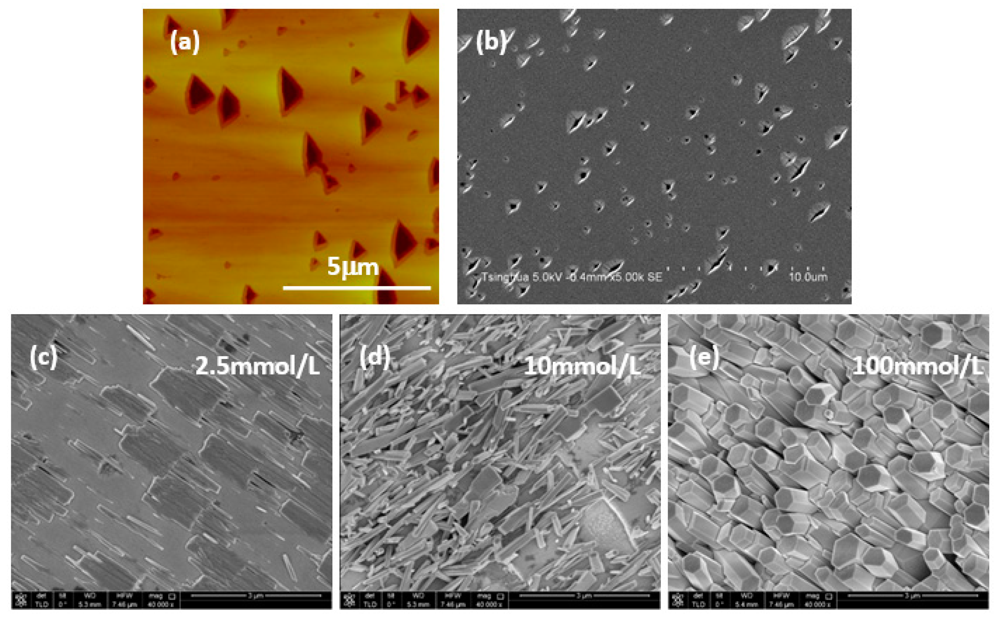
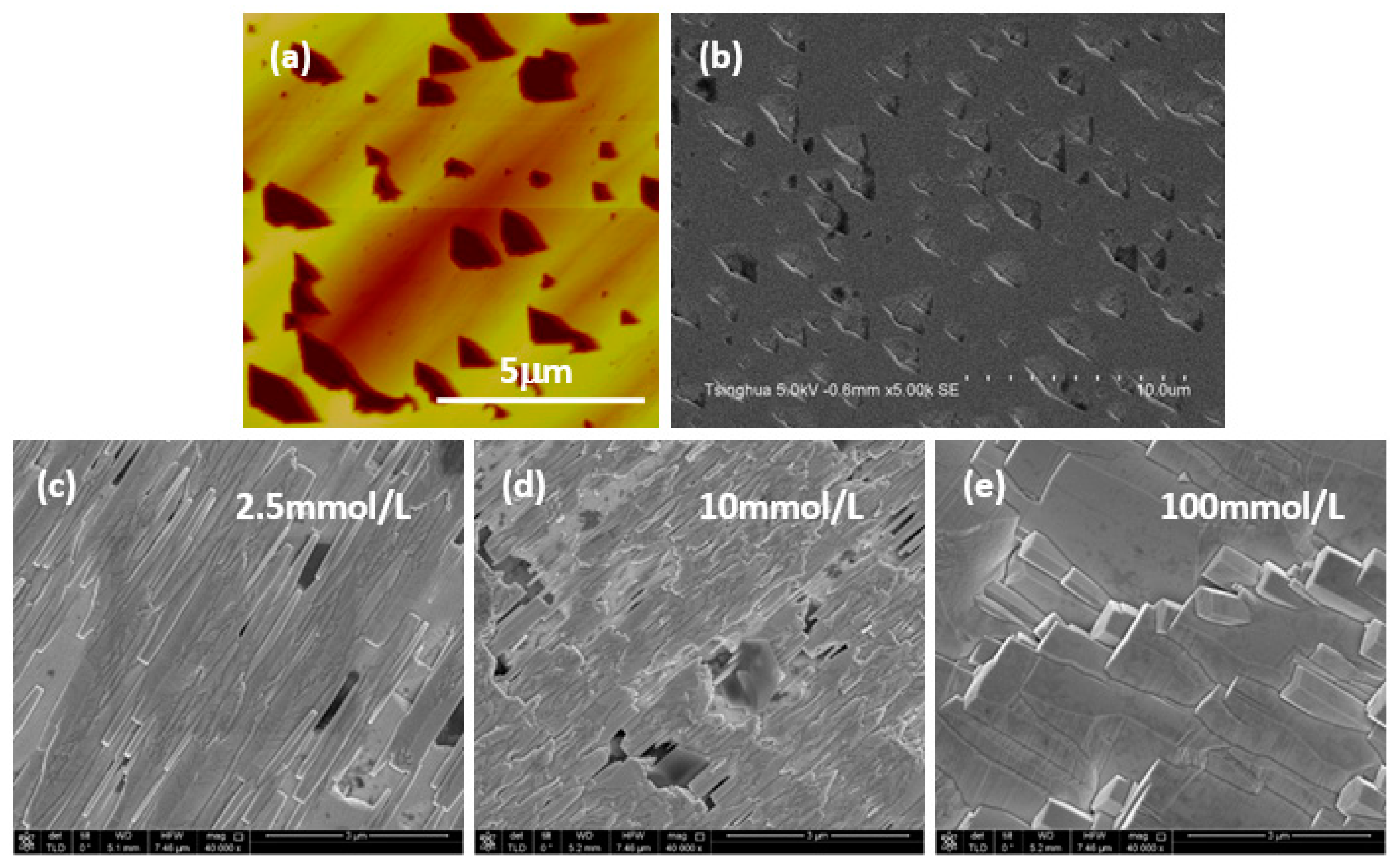
Large triangular surface pits are the typical surface morphology for a-plane GaN [
23], which were produced by incomplete nucleation islands coalescence.
Figure 1a is the AFM image in a 10 μm × 10 μm sampling area, and
Figure 1b is the SEM image of an a-plane GaN grown at 915 °C. It could be seen that there were some randomly distributed triangular surface pits bound by the inclined
and vertical (0001) facets with sizes ranging from 500 nm~2 μm. When the solution concentrations were 2.5 mmol/L and 10 mmol/L, ZnO turned to grow into a thin film, as shown in
Figure 1c,d. As the solution concentration increased to 100 mmol/L, ZnO NWs formed along the (0001) direction on the surface of a-plane GaN, as shown in
Figure 1e. The ZnO NW array distribution just copied the surface pits distribution of GaN. However, it is interesting to see that on another a-plane GaN grown under low temperature (865 °C), as the size and density of the large triangular surface pits increased, ZnO NWs were not formed irrespective of the solution concentration, as shown in
Figure 2.
3.2. ZnO NWs on Semipolar GaN
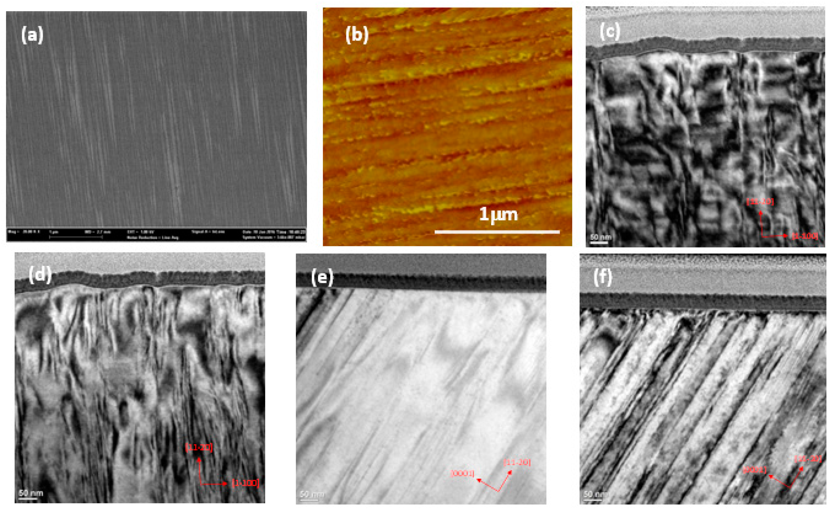
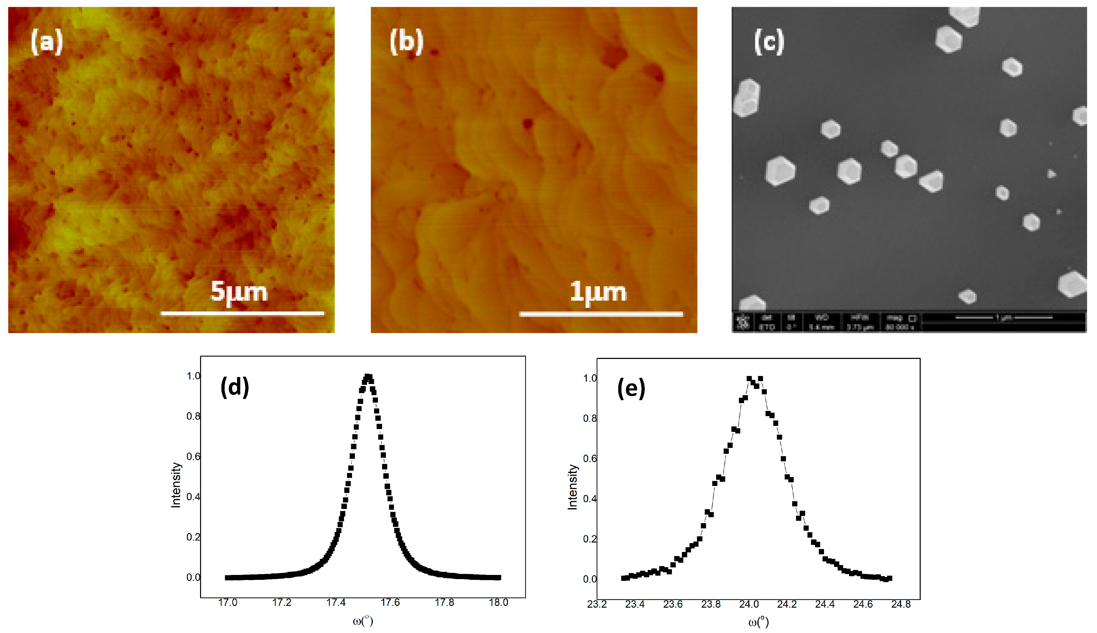
Figure 3a shows the SEM image of the surface morphology of
semipolar GaN. There were ripples along the
direction, which were caused by anisotropic incorporation probability and diffusion length of reaction atoms in the growth front [
24]. Observed from the AFM image, these ripples were decorated with sags and crests, as shown in
Figure 3b. Observed by the cross-sectional TEM image in
Figure 3c,d, these sags were tiny surface pits that connected with dislocations. The defect type was identified to be Shockley type partial dislocation (PD) with
by taking images under different diffraction vectors
according to the invisible criteria [
29], as shown in
Figure 3c–f. When
, the visible defects were Frank–Shockley type PD with
and
and Shockley type PD with
and
. When
, the visible defects were Frank–Shockley type PD with
and Frank type PD with
. When
, the visible defects were basal plane stacking faults (BSFs), I
1 type with
, and I
2 type with
), Frank–Shockley type PD with
, and Shockley type PD with
.
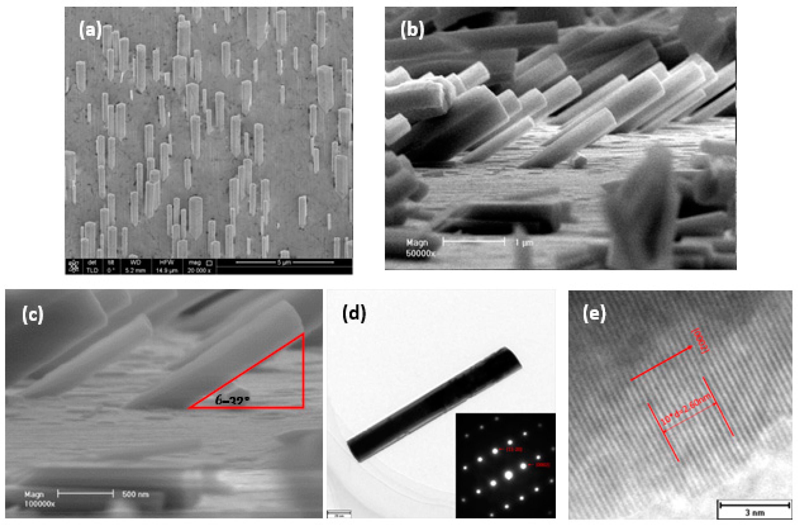
ZnO NWs were grown obliquely upward on (
GaN at an angle of
, as observed in the SEM images in
Figure 4a–c.
Figure 4d is the TEM image of a single ZnO nanowire, where the diffraction spots shown in the inset are bright and sharp. It could be seen that NW was a hexagonal single crystal.
Figure 4e shows the high-resolution TEM image, proving that the nanowire has good crystallinity and grows along the c-axis with lattice constant d of 2.6 Å.
3.3. ZnO NWs on Polarized GaN
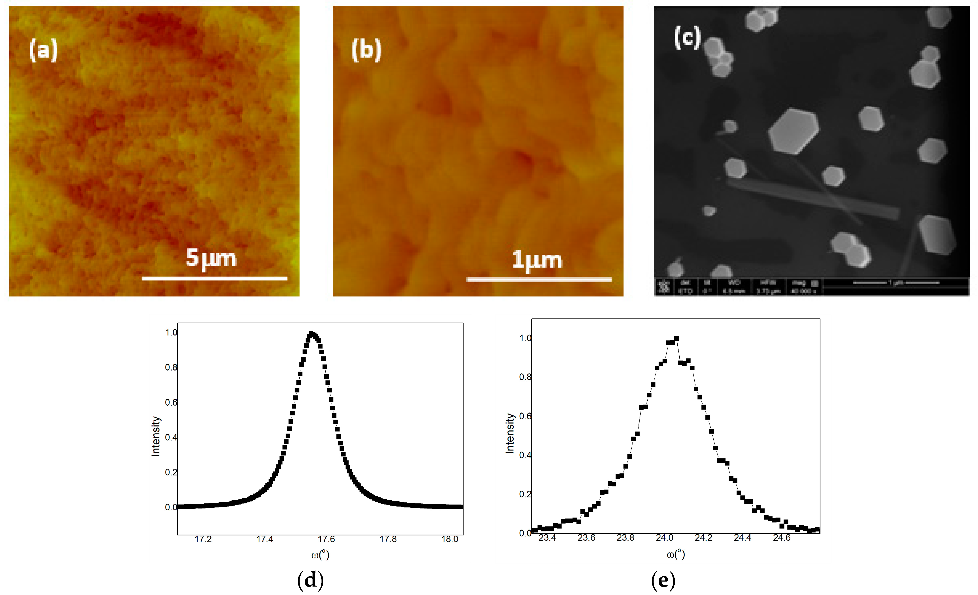
c-plane GaN is much smoother than a-plane GaN; however, there were still some of the small hexagonal surface pits formed at the intersection positions of surface steps, as could be seen from the AFM image in
Figure 5a,b. It is generally accepted that these pits are formed when threading screw dislocations extending to the surface [
25]. The pit density was 1.25 × 10
8 cm
−2. The (002) full width at half maxima (FWHM) of the XRD rocking curve of this sample was 0.144°, and the (102) FWHM was 0.419°. Under low growth temperatures, these small surface pits became more significant, as shown in
Figure 6a,b. Its pit density increased to 1.50 × 10
9 cm
−2, while its (002) FWHM of the XRD rocking curve of this sample decreased to 0.138°, and the (102) FWHM reduced to 0.369°. As for the ZnO NW grown on these two kinds of GaN substrates (
Figure 5c and
Figure 6c), it is interesting to note that the NW density showed a slight increase from 9.4 × 10
−7 cm
−2 to 1.25 × 10
8 cm
−2 with increased surface pits in GaN. The symmetric (002) reflection is related to tilt caused by screw component dislocation for c-plane GaN, and the asymmetric reflection (102) contains the information of the twist produced by edge component dislocation [
30]. NW density did not show a strong correlation with the XRD FWHM, partially because not all dislocations could propagate to the surface and produce a pit, where some may bend or annihilate with each other [
26].
3.4. ZnO NWs on AlxGa1−xN
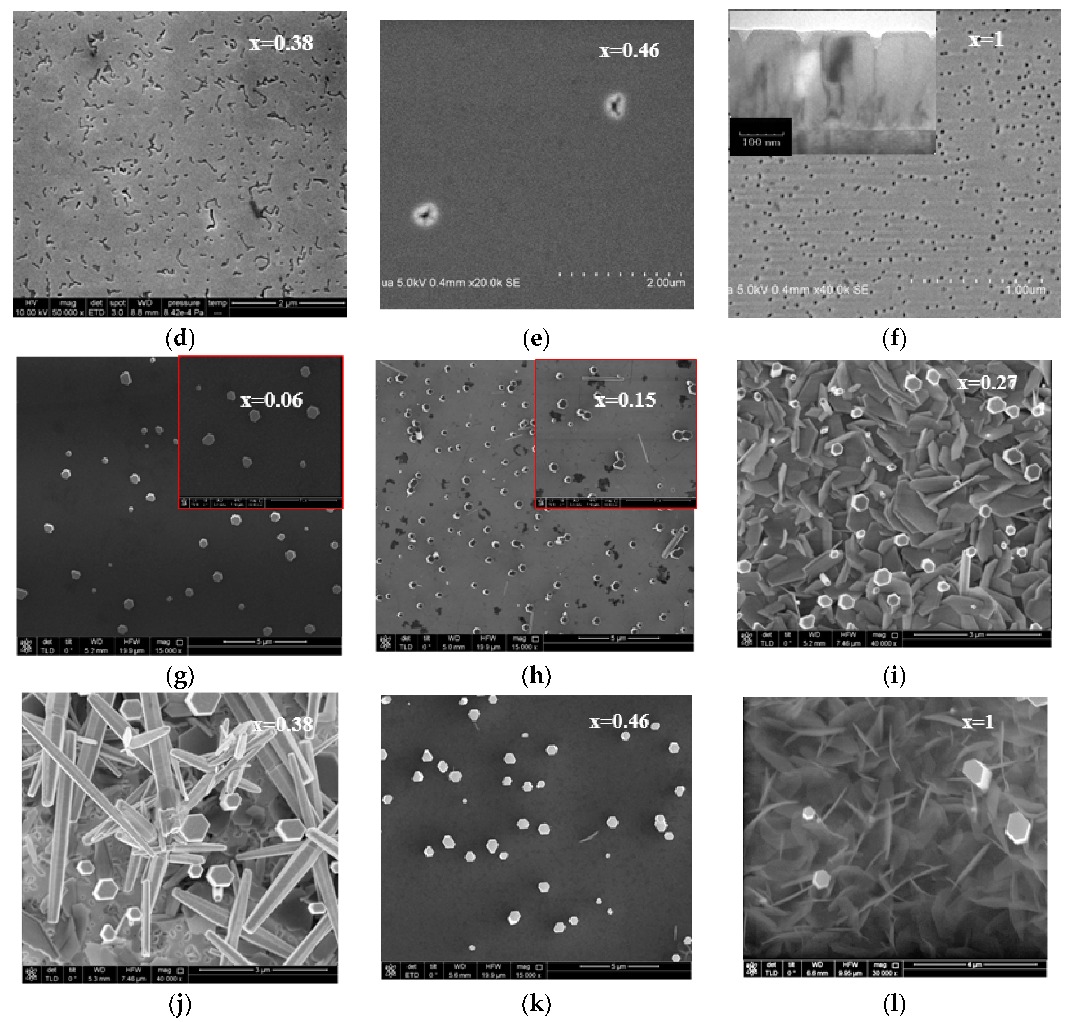
When the Al composition x varied from 0.06 to 1, the Al
xGa
1-xN surface morphology changed significantly, and the ZnO nanostructure on top of it changed accordingly, as shown in
Figure 7.
Table 1 summarizes the variation of Al
xGa
1−xN surface morphology, the types of ZnO nanostructure, and the NWs density.
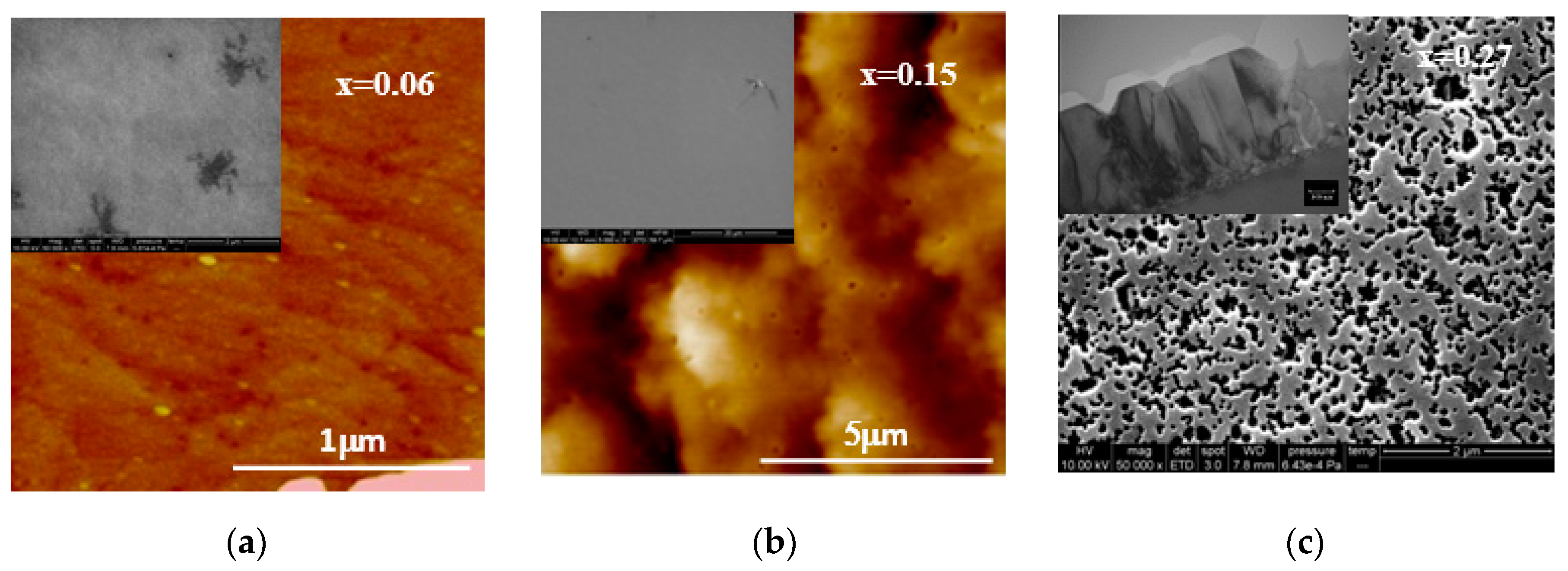
The surface morphology of Al
0.06Ga
0.94N was similar to that of c-plane GaN. Atomic surface steps could be seen in the AFM image, as shown in
Figure 7a. The inset is the SEM image of this sample. There is no contrast in this SEM image. The black spots are carbon contaminations. However, the ZnO NW density on top of the Al
0.06Ga
0.94N (
Figure 7g) was one order of magnitude lower than that on c-plane GaN. When the Al composition increased to 0.15, its surface morphology deteriorated. There was still no contrast in the SEM image (inset of
Figure 7b), but in the AFM image, there were uniformly distributed small surface pits, as shown in
Figure 7b. ZnO NW density grown on top of the Al
0.15Ga
0.85N sample increased significantly, as shown in
Figure 7h.
When the Al composition achieved 0.27, the film was not intact. There were large surface pits together with irregularly shaped grooves on the surface, as shown in
Figure 7c. The inset is the cross-sectional TEM image of the sample, showing that the pits were connected with threading dislocations, and the groove had not expanded to the sapphire substrate. As for the ZnO nanostructures grown on top of the Al
0.27Ga
0.73N, it is interesting to note that in addition to NWs, there were nanosheets, as shown in
Figure 7i. The nanosheets covered the entire surface of Al
0.27Ga
0.73N. When the Al composition further increased to 0.38, the surface pits and irregularly shaped grooves decreased, as shown in
Figure 7d. There were also ZnO nanosheets grown on top of this Al
0.38Ga
0.62N (
Figure 7j), but they did not cover the entire surface. In addition, the ZnO NWs density also decreased.
When the Al composition was 0.46, the surface became smooth again, as shown in
Figure 7e. This agreed with the literature that the Al
0.54Ga
0.46N alloy showed the best crystal quality and surface morphology [
27]. The ZnO nanosheets disappeared (
Figure 7k), and the NW density was maintained as that on Al
0.38Ga
0.62N. As Al composition further increased, its surface morphology deteriorated again. As shown in
Figure 7f, the surface was full of pits in AlN, which could be reduced by increasing the growth temperature [
28,
29]. However, ZnO nanosheets could be produced on this pitted surface, as shown in
Figure 7l. Compared with the nanosheets on the Al
0.27Ga
0.82N surface, more of the ZnO nanosheets were vertically aligned on the AlN surface.
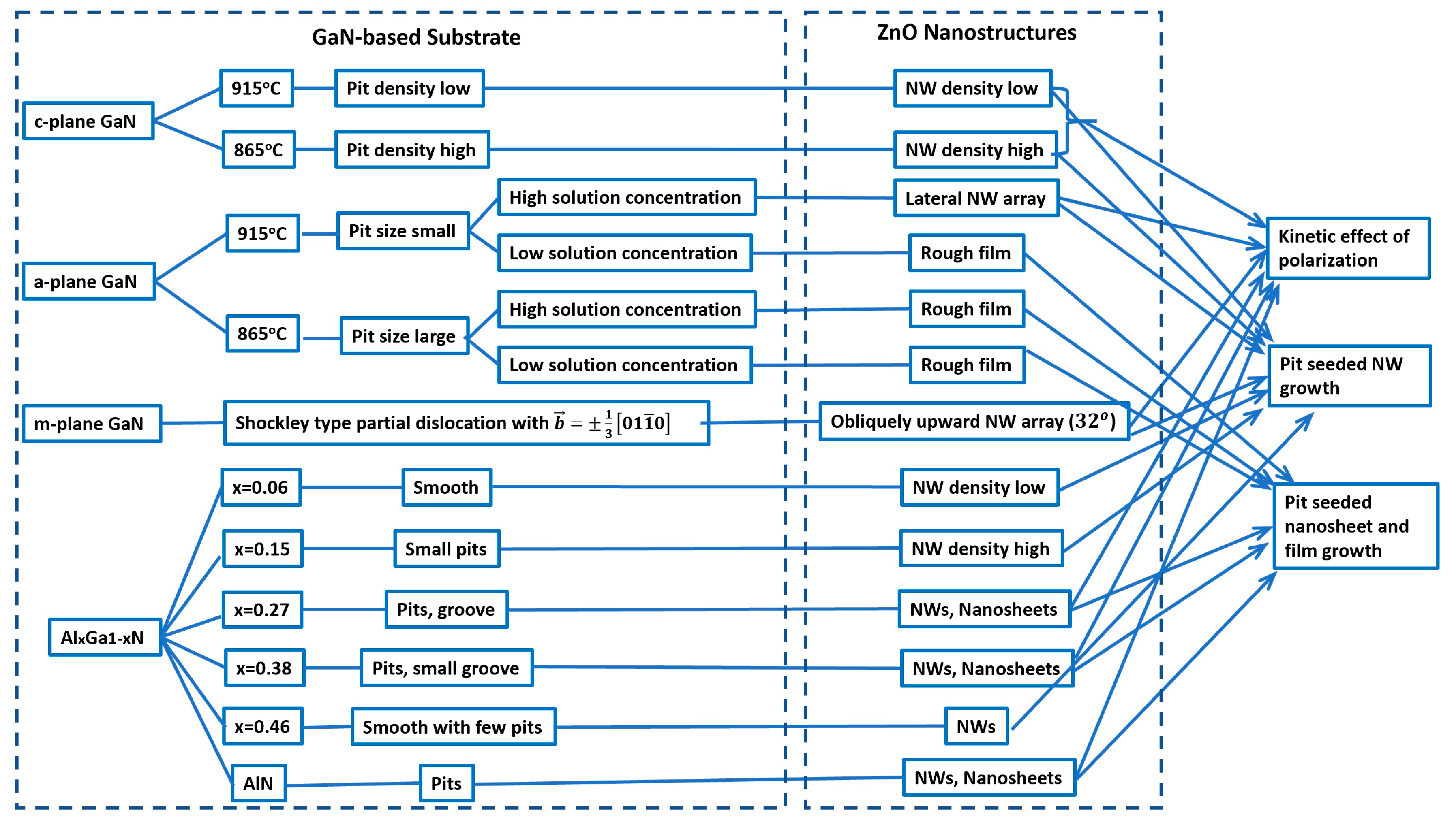
4. Discussion
Through comparing ZnO nanostructure grown on various GaN and Al
xGa
1-xN substrates, it could be seen that the kinetic effect of polarization and surface pits played an important role. Polarization is the intrinsic property that influences growth, while surface pits provide necessary nucleation sites that can be controlled.
Figure 8 summarizes the results and comparison procedure.
4.1. Kinetic Effect of Polarization
The reason for the ZnO NW preferential growth along the c-axis is generally believed to be the anisotropic surface energies [
19,
20,
21]. Since the (0001) plane of ZnO possesses the minimum energy amongst all its lattice planes, high growth speed will be along the c-axis. However, the surface energies for the (0001) and (10-10) planes of ZnO are 2.15 J/m
2, and 1.15 J/m
2, respectively [
31]. According to the free energy minimization principle, the aspect ratio of ZnO NWs should be approximately 2:1, which is not the case; the aspect ratio of ZnO NWs would be at least 10:1. This is because the free energy minimization principle is based on equilibrium conditions and fits homogeneous nucleation. The kinetic and substrate factors have not been considered.
In many cases, surface charges and polarization have been considered as the driving force of many nanostructures, such as ZnO nanosprings and nanorings [
1] and AlN nanonecklaces and CrSi
2 nanowebs [
32]. Until now, it has not been reported how polarization influences hydrothermal growth in a kinetic view. We proposed that in the ZnO hydrothermal process, the spontaneous polarization field could help to separate NH
4+ and OH
− near the growing surface, so as to accelerate the decomposition of
NH3 ·
H2O ↔
NH4+ +
OH−. Thus, nucleation would be at the polarized surface of the substrate. In further growth, the polarization filed that already established in ZnO NWs would also attract OH
− anions and accelerate preferential growth along the polarization direction.
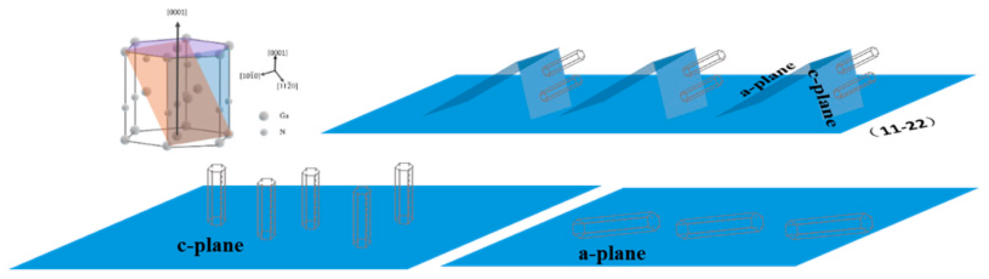
Comparing the ZnO NWs directly grown on a-plane, c-plane, and (11-20) plane GaN substrate could demonstrate this. It could be seen that in all lattice orientations, ZnO NWs nucleated from the polarized facet of GaN and grew along the c-axis.
Figure 9 schematically illustrates this. Although a-plane GaN was nonpolar, there were many large surface pits bound by the (0001) polarized facet. So, ZnO NWs seemed to grow laterally on the substrate. In the semipolar sample, ZnO NWs were grown obliquely upward on (
) GaN with an angle of
θ = 32°, which was the value of the angle between the GaN c-axis and (
plane of GaN, indicating that growth was along the polarized direction of the GaN substrate.
In the Al
xGa
1-xN sample, since aluminum is an amphoteric metal, it can be dissolved into the solution under alkaline conditions in the presence of ammonia, and Al(OH)
4− ions are first formed by the reaction between OH
− and the substrate [
33]. Al(OH)
4− would presumably bind to the Zn
2+ terminated polarized surface and suppress the kinetic effect of the polarization field. As a result, NW density in AlGaN was comparatively smaller than that in GaN samples. In the samples where the polarized surfaces were not intact, such as Al
0.27Ga
0.73N, lateral growth of ZnO was triggered, and nanosheets were formed, as shown in
Figure 7i. In AlN, although the polarized surface had not been destroyed by pits, ZnO nanosheets still formed because there were more Al atoms to bind to the Zn
2+ terminated surface to suppress the kinetic effects of the polarization field.
4.2. Surface Pits vs. Dislocation
It was reported that screw dislocation defects provide self-perpetuating growth steps to enable the anisotropic growth of various nanomaterials at low supersaturation [
17]. However, note that screw dislocation is typically connected with surface pits when propagated to the crystal surface. In fact, screw dislocation defects could provide self-perpetuating growth steps lying in that screw dislocation, which would cause a surface displacement equal to the component of the Burgers vector normal to the surface in order to achieve a balance between the surface energy and dislocation strain energy, according to the classical dislocation mediating growth theory proposed by Frank. This step-growth around the screw dislocation core would result in an inverted pyramid pit on the free surface [
34], as observed in many materials, including GaN [
25]. We believed that it was the surface pit that seeded for NW growth. It could be seen that on the c-plane GaN substrate, more significantly pitted GaN surfaces yielded higher ZnO NW density, as comparatively shown in
Figure 5 and
Figure 6. In contrast, ZnO NW density did not show correlations with the dislocation density of GaN observed by XRD. Since the pits on the GaN surface can be produced either by screw component dislocation or by other mechanisms, such as incomplete island coalescence, dislocation is not the driving force for ZnO NW growth on GaN substrate. It could be seen that ZnO NWs grew from sites of the large surface pits of a-plane GaN (
Figure 1e), which were produced by incomplete nucleation islands coalescence. For the AlGaN substrate samples, although the mismatch between Al
0.06Ga
0.954N and ZnO was smaller than that between Al
0.15Ga
0.85N and ZnO, ZnO NW density grown on Al
0.15Ga
0.85N was higher than that on Al
0.06Ga
0.954N because there were more surface pits in Al
0.15Ga
0.85N.
The reason for surface pits to serve as nucleation sites is because the solid-liquid reaction takes place at the interface between the two phases, and the solid surface properties determine the densities and structure of the active centers. Atomic-level steps, terraces, and kinks would be the nucleation centers according to the terrace-step-kink (TSK) model [
35]. Since GaN surface pits were composed of the terrace, steps, and kinks, they were the excellent nucleation sites for NW growth. From the catalytic point of view, these sites have higher catalytic activity, and nucleation can preferentially occur in the pits under low super-saturation.
Not only screw dislocations, but PD could also produce surface pits to serve as nucleation sites, as in the (
) semipolar GaN, shown in
Figure 3b. Those small pits enable the surface full of sags and crests, which are similar to the granular morphology of the ZnO seed layer. The functions of the ZnO seed layer on a substrate in hydrothermal growth are to provide matched lattice and nucleation sites [
36,
37]. Correspondingly, the uniformly distributed small pits on the GaN surface serve the same function as the ZnO seed layer. This can provide a way to directly grow ZnO NW on the GaN substrate by controlling the surface pits in GaN.
Note that surface pits were the nucleation sites not only for NW growth but also for ZnO nanosheets and film. For AlN, the surface pits were the nucleation sites for nanosheets, as shown in
Figure 7f,l. Under low solution concentrations, ZnO formed a roughened film on the a-plane GaN surface, as shown in
Figure 1c and
Figure 2c. In addition, it should be pointed out that the pit size and density should be controlled. If the GaN surface pit was large enough, and its density was high enough, ZnO NW tended to grow laterally and connected with each other to produce a film with a rough surface, even under high solution concentrations, as shown in
Figure 2e.
5. Conclusions
The growth of ZnO NWs directly grown on GaN-based materials is a combination of many factors, such as polarization, small lattice mismatch, and high density of defects in GaN. Polarization took effect through the kinetic process of hydrothermal growth of ZnO. Dislocation in GaN affected ZnO NW growth through the surface pits. More specifically:
1. Since there were big surface pits in a-plane GaN, c-axis ZnO NW could grow from the polarized side facet of the pit and laterally align on GaN. However, if the pit size was too large, ZnO NWs would grow laterally and merge to form a film.
2. Uniformly distributed small surface pits in () GaN, which were produced by PD with when propagated to the surface, could seed ZnO NW growth. ZnO NWs grew obliquely upward on ( GaN at an angle of , which was the polarized orientation.
3. c-plane GaN with more surface pits yielded more ZnO NWs, while the GaN FWHM of the XRD rocking curve did not show strong correlations with NW density.
4. Al0.15Ga0.85N with more lattice mismatch with ZnO than Al0.06Ga0.954N gained more ZnO NWs on its top because there were more surface pits in Al0.06Ga0.95N. When the polarized surface of AlGaN was not intact, such as Al0.27Ga0.73N, nanosheets were formed.
5. In AlN, surface pits served as seeds to grow nanosheets since Al(OH)4− would presumably bind to the Zn2+ terminated polarized surface and suppress the kinetic effects of the polarization field.
Author Contributions
Conceptualization, Z.G.; methodology, Z.G. and X.X.; formal analysis, L.L., L.Z., J.L., and H.L.; writing—original draft preparation, Z.G.; writing—review and editing, D.A.
Funding
This work was supported by the National Natural Science Foundation of China (Grant No. 11204009), Beijing Municipal Natural Science Foundation (Grant No.4142005 and No.4182014), and Beijing Education Commission Science and Technology Program (Grant No. KM201810005025).
Acknowledgments
Thank you Beijing Kexin Haoyu Technology Co. Ltd. for providing quick electron microscopy measurements.
Conflicts of Interest
The authors declare no conflict of interest. The funders had no role in the design of the study; in the collection, analyses, or interpretation of data; in the writing of the manuscript, or in the decision to publish the results.
References
- Kong, X.Y.; Ding, Y.; Yang, R.S.; Wang, Z.L. Single-crystal nanorings formed by epitaxial self-coiling of polar nanobelts. Science 2004, 303, 1348. [Google Scholar] [CrossRef] [PubMed] [Green Version]
- Xi, Y.; Guo, H.Y.; Zi, Y.; Li, X.; Wang, J.; Deng, J.; Li, S.; Hu, C.; Cao, X.; Wang, Z.L. Multifunctional TENG for blue energy scavenging and self-powered wind speed sensor. Adv. Energy Mater. 2017, 7, 1602397. [Google Scholar] [CrossRef]
- Dogar, S.; Khan, W.; Kim, S.D. Ultraviolet photoresponse of ZnO nanostructured AlGaN/GaN HEMT. Mater. Sci. Semicond. Process. 2016, 44, 71–77. [Google Scholar] [CrossRef]
- Lee, C.T.; Chiu, Y.S. Piezoelectric ZnO-nanorod-structured pressure sensors using GaN-based field-effect-transistor. Appl. Phys. Lett. 2015, 106, 073502. [Google Scholar] [CrossRef]
- Lupan, O.; Pauporté, T.; Vianac, B.; Aschehougc, P. Electrodeposition of Cu-doped ZnO NW arrays and heterojunction formation with p-GaN for color tunable light emitting diode applications. Electrochim. Acta 2011, 56, 10543–10549. [Google Scholar] [CrossRef]
- Yu, C.H.; Li, R.; Li, T.B.; Dong, H.L.; Jia, W.; Xu, B.S. Effect of in doping on the photoelectric properties of n-ZnO nanorods p-GaN heterojunction LED. Superlattices Microstruct. 2018, 120, 298–304. [Google Scholar] [CrossRef]
- Li, H.X.; Zhao, W.Q.; Liu, Y.; Liang, Y.; Ma, L.; Zhu, M.; Yi, C.J.; Xiong, L.; Gao, Y.H. High-level-Fe-doped p-type ZnO nanowire array/n-GaN film for UV-free white LED. Mater. Lett. 2019, 239, 45–47. [Google Scholar] [CrossRef]
- Peng, Y.Y.; Que, M.L.; Lee, H.E.; Bao, R.R.; Wang, X.D.; Lu, J.F.; Yuan, Z.Q.; Li, X.Y.; Tao, J.; Sun, J.L.; et al. Achieving high resolution pressure mapping via flexible GaN/ZnO nanowire LEDs array by piezo-phototronic effect. Nano Energy 2019, 58, 633–640. [Google Scholar] [CrossRef]
- Chen, C.H.; Chang, S.J.; Chang, S.P.; Li, M.J.; Chen, I.; Hsueh, T.J.; Hsu, C.L. Novel fabrication of UV photodetector based on ZnO NW/p-GaN heterojunction. Chem. Phys. Lett. 2009, 476, 69–72. [Google Scholar] [CrossRef]
- Mai, W.J.; Gao, P.X.; Lao, C.S.; Wang, Z.L.; Sood, A.K.; Polla, D.L.; Soprano, M.B. Vertically aligned ZnO NW arrays on GaN and SiC substrates. Chem. Phys. Lett. 2008, 460, 253–256. [Google Scholar] [CrossRef]
- Mishra, M.; Gundimeda, A.; Garg, T.; Dash, A.; Das, S.; Gupta, G. ZnO/GaN heterojunction based self-powered photodetectors: Influence of interfacial states on UV sensing. Appl. Surf. Sci. 2008, 478, 1081–1089. [Google Scholar] [CrossRef]
- Zhou, H.; Gui, P.B.; Yang, L.; Ye, C.; Xue, M.N.; Mei, J.; Song, Z.H.; Wang, H. High performance self-powered UV photodetector based on a ZnO nanoarrays/GaN structure with a CdS insert layer. New J. Chem. 2017, 41, 4901–4907. [Google Scholar] [CrossRef]
- Abdulgafour, H.I.; Hassan, Z.; Yam, F.K.; Chin, C.W. Sensing devices based on ZnO hexagonal tube-like nanostructures grown on p-GaN heterojunction by wet thermal evaporation. Thin Solid Films 2013, 540, 212–220. [Google Scholar] [CrossRef]
- So, H.Y.; Senesky, D.G. ZnO nanorod arrays and direct wire bonding on GaN surfaces for rapid fabrication of antireflective, high-temperature ultraviolet sensors. Appl. Surf. Sci. 2016, 387, 280–284. [Google Scholar] [CrossRef]
- Chew, Z.J.; Brown, R.A.; Maffeis, T.G.G.; Li, L.J. Comparison of ZnO nanowires synthesized on various surfaces on a single substrate. Mater. Lett. 2012, 72, 60–63. [Google Scholar] [CrossRef]
- Wang, X.; Song, J.; Li, P.; Ryou, J.H.; Dupuis, R.D.; Summers, C.J.; Wang, Z.L. Growth of Uniformly Aligned ZnO Nanowire Heterojunction Arrays on GaN, AlN, and Al0.5Ga0.5N Substrates. J. Am. Chem. Soc. 2005, 127, 7920–7923. [Google Scholar] [CrossRef] [PubMed]
- Meng, F.; Morin, S.A.; Forticaux, A.; Jin, S. Screw dislocation driven growth of nanomaterials. Acc. Chem. Res. 2013, 46, 1616–1626. [Google Scholar] [CrossRef]
- Morin, S.A.; Jin, S. Screw dislocation driven epitaxial solution growth of ZnO nanowires seeded by dislocations in GaN substrates. Nano Lett. 2010, 10, 3459–3463. [Google Scholar] [CrossRef]
- Kim, D.S.; Gosele, U.; Zacharias, M. Surface diffusion induced growth of ZnO nanowires. J. Cryst. Growth 2009, 311, 3216–3219. [Google Scholar] [CrossRef]
- Chen, C.W.; Pan, C.J.; Tsao, F.C.; Liu, Y.L.; Kuo, C.W.; Kuo, C.H.; Chi, G.C.; Chen, P.H.; Lai, W.C.; Hsueh, T.H.; et al. Catalyst free ZnO nanowires grown on a-plane GaN. Vacuum 2010, 84, 803–806. [Google Scholar] [CrossRef]
- Sahoo, T.; Choi, J.H.; Yoo, J.W.; Yu, Y.T.; Jeon, S.R.; Baek, J.H.; Yoon, H.D.; Hwang, S.M.; Lee, I.H. Hydrothermal growth of ZnO nanorods on a-plane GaN/sapphire template. J. Cryst. Growth 2010, 312, 2857–2860. [Google Scholar] [CrossRef]
- Nandi, R.; Srinivasa, R.S.; Major, S.S. Morphology and photoluminescence of ZnO nanorods grown on sputtered GaN films with intermediate ZnO seed layer. Mater. Chem. Phys. 2016, 182, 155–166. [Google Scholar] [CrossRef]
- Gao, Z.Y.; Li, J.J.; Xue, X.W.; Cui, B.F.; Xing, Y.H.; Zou, D.S. Different structural origins for different sized surface pits observed on a-plane GaN film. Sci. China 2016, 59, 156–161. [Google Scholar] [CrossRef]
- Xu, S.R.; Lin, Z.X.; Xue, X.Y.; Liu, Z.Y.; Ma, J.C.; Jang, T.; Mao, W.; Wang, D.H.; Zhang, J.C.; Hao, Y. Comparative study on characteristics of basal plane stacking faults of nonpolar a plane and semipolar 11-22 GaN. Chin. Phys. Lett. 2012, 29, 017803. [Google Scholar] [CrossRef]
- Heying, B.; Tarsa, E.J.; Elsass, C.R.; Fini, P.; DenBaars, S.P.; Speck, J.S. Dislocation Mediated Surface Morphology of GaN. J. Appl. Phys. 1999, 85, 6470–6476. [Google Scholar] [CrossRef]
- Gao, Z.Y.; Xue, X.W.; Li, H.M.; Li, J.J.; Ma, L.; Wu, W.R.; Zou, D.S. Influence of lateral growth on the surface pit formation of GaN heteroepitaxial film grown by MOCVD. Mater. Sci. 2016, 22, 223–227. [Google Scholar] [CrossRef] [Green Version]
- Liu, B.; Zhang, R.; Xie, Z.L.; Liu, Q.J.; Zhang, Z.; Li, Y.; Xiu, X.Q.; Yao, J.; Mei, Q.; Zhao, H.; et al. Al incorporation, structural and optical properties of AlxGa1−xN (0.13 ≤ x ≤ 0.8) Alloys grown by MOCVD. J. Cryst. Growth 2008, 310, 4499–4502. [Google Scholar] [CrossRef]
- Zhang, D.G.; Li, Z.H.; Peng, D.Q.; Dong, X.; Li, C.H. Temperature dependence of the character of AlN nucleation layer grown on SiC substrates by MOCVD. Superlattices Microstruct. 2016, 99, 104–107. [Google Scholar] [CrossRef]
- Kong, B.H.; Sun, Q.; Han, J.; Lee, I.; Cho, H.K. Classification of stacking faults and dislocations observed in nonpolar a-plane GaN epilayers using transmission electron microscopy. Appl. Surf. Sci. 2012, 258, 2522–2528. [Google Scholar] [CrossRef]
- Chierchia, R.; Bottcher, T.; Heinke, H.; Einfeldt, S.; Figge, S.; Hommel, D. Microstructure of Heteroepitaxial GaN Revealed by X-ray Diffraction. J. Appl. Phys. 2003, 93, 8918–8925. [Google Scholar] [CrossRef]
- Meyer, B.; Mark, D. Density-functional study of the structure and stability of ZnO surfaces. Phys. Rev. B 2003, 67, 035403. [Google Scholar] [CrossRef] [Green Version]
- Wang, H.T.; Wu, T. Formation of complex nanostructures driven by polar surfaces. J. Mater. Chem. 2011, 21, 15095. [Google Scholar] [CrossRef]
- Lin, Y.; Jiang, Q.F. Effect of substrates and anions of zinc salts on the morphology of ZnO nanostructures. Appl. Surf. Sci. 2011, 257, 8728–8731. [Google Scholar] [CrossRef]
- Frank, F.C. Capillary equilibria of dislocated crystals. Acta Cryst. 1951, 4, 497–501. [Google Scholar] [CrossRef]
- Ibach, H. Physics of Surface and Interfaces; Springer: Berlin, Germany, 2006. [Google Scholar]
- Greene, L.E.; Law, M.; Tan, D.H.; Montano, M.; Goldberger, J.; Somorjai, G.; Yang, P.D. General goute to vertical ZnO nanowire arrays using textured ZnO seeds. Nano Lett. 2005, 5, 1232–1236. [Google Scholar] [CrossRef] [PubMed]
- Song, J.; Lim, S. Effect of seed layer on the growth of ZnO nanorods. J. Phys. Chem. C 2007, 111, 596–600. [Google Scholar] [CrossRef]
Figure 1.
(a) 10 μm × 10 μm AFM image and (b) SEM image of the surface morphology of a-plane GaN grown under the temperature of 915 °C. The large triangle surface pit density was 9.1 × 106 cm−2. (c,d) SEM images of ZnO grown on this a-plane GaN substrate under the solution concentration of 2.5 mmol/L and 10 mmol/L, respectively. (e) SEM image of ZnO NW (nanowire) array grown on this a-plane GaN substrate under the solution concentration of 100 mmol/L.
Figure 2.
(a) 10 μm × 10 μm AFM image and (b) SEM image of the surface morphology of a-plane GaN grown under the temperature of 865 °C. The large triangle surface pit density was 9.7 × 106 cm−2. (c–e) SEM images of ZnO grown on this a-plane GaN substrate under the solution concentration of 2.5 mmol/L,10 mmol/L, and 100 mmol/L, respectively.
Figure 3.
(a) SEM image and (b) 2 μm × 2 μm AFM image of the surface morphology of (11-22) semi-polar GaN; Cross-sectional two-beam bright-field TEM images using (c) and (d) near the zone axis, and using (e) and (f) near the zone axis.
Figure 3.
(a) SEM image and (b) 2 μm × 2 μm AFM image of the surface morphology of (11-22) semi-polar GaN; Cross-sectional two-beam bright-field TEM images using (c) and (d) near the zone axis, and using (e) and (f) near the zone axis.
Figure 4.
(
a) SEM image of ZnO NWs grown on the semipolar (
GaN using the sample of
Figure 3. (
b) Cross-sectional SEM image of the ZnO NWs array. (
c) Analysis of the angle between ZnO NW and GaN substrate. (
d) The TEM image of a single ZnO nanowire grown on (
GaN surface, inset is its diffraction pattern; (
e) high-resolution TEM image showing interplanar spacing of (0001) lattice plane in ZnO.
Figure 5.
AFM image of the surface morphology of the c-plane GaN grown under the temperature of 915 °C: (a) 10 μm × 10 μm sampling area and (b) 2 μm × 2 μm sampling area. (c) SEM image of ZnO NWs grown on this polarized GaN substrate under the concentration of 10 mmol/L. (d) XRD rocking curve of (002) reflection. (e) XRD rocking curve of (102) reflection.
Figure 6.
AFM image of the surface morphology of the c-plane GaN grown under the temperature of 865 °C: (a) 10 μm × 10 μm sampling area and (b) 2 μm × 2 μm sampling area. (c) SEM image of ZnO NWs grown on this polarized GaN substrate under the concentration of 10 mmol/L. (d) XRD rocking curve of (002) reflection. (e) XRD rocking curve of (102) reflection.
Figure 7.
(a) 2 μm × 2 μm AFM image of Al0.06Ga0.94N, inset is the corresponding SEM image; (b) 10 μm × 10 μm AFM image of Al0.15Ga0.85N, inset is the corresponding SEM image; (c) SEM image of Al0.27Ga0.78N, inset is the cross-sectional TEM image; (d) SEM image of Al0.38Ga0.62N; (e) SEM image of Al0.46Ga0.54N; (f) SEM image of AlN, inset is the cross-sectional TEM image; (g) SEM image of ZnO NWs grow on Al0.06Ga0.94N, inset is the image under large magnification; (h) SEM image of ZnO NWs grown on Al0.15Ga0.85N, inset is the image under large magnification; (i) SEM image of ZnO NWs and nanosheets grown on Al0.27Ga0.78N; (j) SEM image of ZnO NWs and nanosheets grown on Al0.38Ga0.62N; (k) SEM image of ZnO NWs grown on Al0.46Ga0.54N; (l) SEM image of ZnO NWs and nanosheets grown on AlN.
Figure 8.
Experimental results and comparison procedure.
Figure 8.
Experimental results and comparison procedure.
Figure 9.
Schematic views of ZnO NWs growth on different lattice orientations of GaN substrate.
Figure 9.
Schematic views of ZnO NWs growth on different lattice orientations of GaN substrate.
Table 1.
Variations of AlxGa1−xN surface morphology and ZnO nanostructure with Al composition of AlxGa1−xN (0.06 ≤ x ≤ 1).
Table 1.
Variations of AlxGa1−xN surface morphology and ZnO nanostructure with Al composition of AlxGa1−xN (0.06 ≤ x ≤ 1).
| Sample | AlxGa1−xN Morphology | ZnO Nano Structure | NW Density, cm−2 |
|---|
| x = 0.06 | Smooth | NWs | 3.6 × 10⁷ |
| x = 0.15 | Small pits | NWs | 1.0 × 10⁸ |
| x = 0.27 | Pits, groove | NWs, nanosheets | 7.9 × 10⁷ |
| x = 0.38 | Pits, small groove | NWs, nanosheets | 3.0 × 10⁷ |
| x = 0.46 | Smooth with few pits | NWs | 3.0 × 10⁷ |
| x = 1.0 | Pits | NWs, nanosheets | 4.9 × 10⁶ |
© 2019 by the authors. Licensee MDPI, Basel, Switzerland. This article is an open access article distributed under the terms and conditions of the Creative Commons Attribution (CC BY) license (http://creativecommons.org/licenses/by/4.0/).

 ,
, 


