Article

Origin of Nanoscale Incipient Plasticity in GaAs and InP Crystal

1
Institute of Materials Engineering, Faculty of Science and Technology, University of Silesia in Katowice, 75 Pułku Piechoty 1A, 40-500 Chorzów, Poland
2
Nordic Hysitron Laboratory, Department of Chemistry & Materials Science, School of Chemical Engineering, Aalto University, Espoo, 00076 Aalto, Finland
3
Institute of Physics, Faculty of Science and Technology, University of Silesia in Katowice, 75 Pułku Piechoty 1A, 40-500 Chorzów, Poland
*
Author to whom correspondence should be addressed.
Crystals 2019, 9(12), 651; https://doi.org/10.3390/cryst9120651
Submission received: 26 October 2019 / Revised: 4 December 2019 / Accepted: 5 December 2019 / Published: 7 December 2019
(This article belongs to the Special Issue Dislocations in Heterostructures)

Abstract

:
In this article, we exhibit the influence of doping on nanoindentation-induced incipient plasticity in GaAs and InP crystals. Nanoindentation experiments carried out on a GaAs crystal show a reduction in contact pressure at the beginning of the plastic deformation caused by an increase in Si doping. Given that the substitutional Si defects cause a decrease in the pressure of the GaAs-I → GaAs-II phase transformation, we concluded that the elastic–plastic transition in GaAs is a phase-change-driven phenomenon. In contrast, Zn- and S-doping of InP crystals cause an increase in contact pressure at the elastic–plastic transition, revealing its dislocation origin. Our mechanical measurements were supplemented by nanoECR experiments, which showed a significant difference in the flow of the electrical current at the onset of plastic deformation of the semiconductors under consideration.

1. Introduction

This paper concerns InP and GaAs semiconductors, which are nowadays widely used in optoelectronics and are essential for the design and fabrication of numerous micro-devices [1]. We focus on a particular phenomenon in semiconducting crystals, namely their transition from an elastic to plastic state. Although it is widely known that an irreversible deformation of defect-free nano-volumes of metallic crystals is linked to the generation of dislocations [2], the case of semiconductors frequently involves phase transformations under the applied high-pressure [3].
The widely accepted method for studying a nanodeformation in various crystalline materials is nanoindentation [4]. The data collected during the measurement can be presented in the form of a load–displacement (P-h) curve, which may show, on the loading part, a characteristic discontinuity. This is what is known as the “pop-in”, which reflects the sudden displacement of the indenter. In the case of a load-controlled experiment, the indenter penetrates the crystal under a constant load.
The first pop-in indicates the beginning of the elastic–plastic transition [5,6], making it possible to determine the contact pressure of this characteristic phenomenon. In order to study the plastic deformation of semiconductors more accurately, nanoelectrical experiments can be carried out. Indeed, using a conductive diamond indenter, the change in the electric current during the elastic–plastic transition can be measured, which is particularly desirable when the appearance of high-pressure, metallic phases is expected.
Data available in the literature show dislocation generation as the cause of incipient plasticity in GaAs and InP crystals. Indeed, microscopic analysis of the plastically deformed volume around the residual impression shows complex displacement patterns [7,8], never revealing a trace of metallic, high-pressure phases. Raman spectra collected from a pristine surface of InP and compared to those obtained at the center of an indent is an example of such investigation [9]. Due to the fact that the above-cited microstructural studies were carried out after nanoindentation, we assumed that it is premature to exclude the influence of phase transformation on the incipient plasticity in GaAs and InP crystals.
In order to determine the phenomenon that initiates plastic deformation in nano-induced GaAs and InP crystals, we examined the effect of doping on their initial plasticity. We expect that the presence of admixtures in the crystal lattice affects the course of both phase transformation and generation of dislocations. Indeed, the presence of Si atoms in the GaAs lattice reduces the pressure of transformation from zincblende (GaAs-I) to rock-salt-like (GaAs-II, Cmcm space group) phase [10]. Similarly, it was also found that Fe-doping of InP decreases the pressure of transformation from zincblende to the rock-salt structure [11], which agrees with the results obtained for Se-doped InP [12]. On the other hand, doping with GaAs and InP causes an increase in microhardness, yield point, and also inhibits the generation of dislocations during crystal growth [13,14,15,16,17,18,19]. In other words, doping of GaAs and InP should increase the shear stress required for the generation of dislocations. Consequently, if the elastic–plastic transition is due to the generation of dislocations, doping should increase the contact pressure at the instant of the pop-in event. The opposite effect is expected when the elastic–plastic transition is caused by a structural phase transformation.

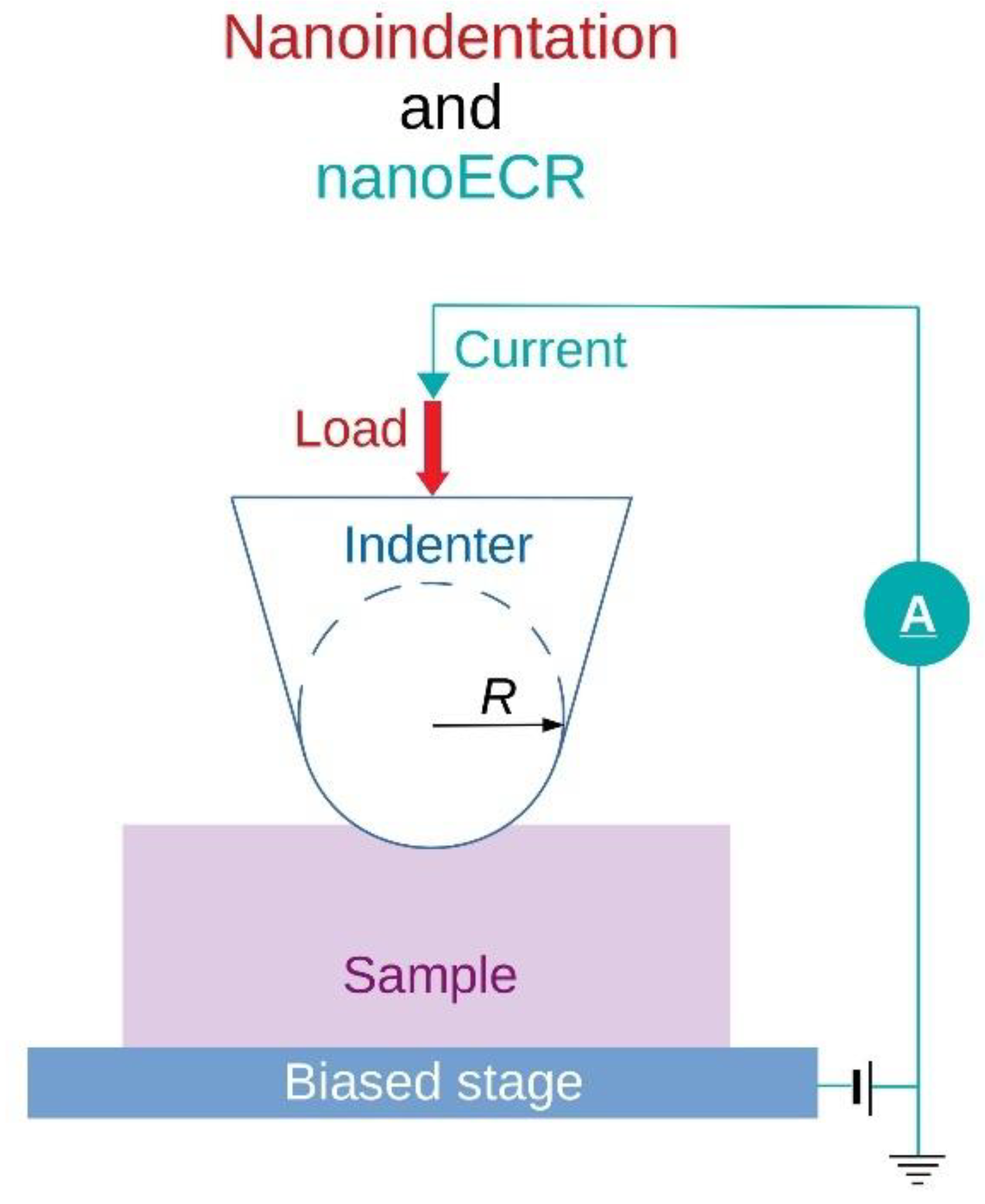
2. Materials and Methods

The (100)-oriented semiconducting crystals, fabricated by the vertical gradient freeze method and used in the present study, were purchased from MTI Corp. (USA). The GaAs specimens were doped by silicon, while the InP crystals were modified by the addition of zinc and sulfur (see Table 1 for details). Load-controlled nanoindentation experiments (Triboindenter TI-950 (Bruker, Billerica, MA, USA)) were carried out using a diamond indenter with a spherical tip (Figure 1). As the dislocations etch pit density was lower than 4000 cm−2, the approximate distance between defects is 150 μm. Such a low density of dislocations in our samples assured us that nanoindentation would be capable of probing both elastic and plastic properties of investigated crystals within a virtually dislocation-free, stressed nanovolume. The experiments were performed under maximum loads of 6 mN and 5 mN, for GaAs and InP, respectively. The used load function consisted of a 5 s loading and equally long unloading path, with a dwell time of 2 s. Consequently, the loading rate equals 6/5 mN/s and 1 mN/s for GaAs and InP, respectively. The measurements of reduced Young’s modulus were performed according to widely accepted Oliver–Pharr method.
The nanoECR (nano Electrical Contact Resistance) measurements were carried out to examine the course of the semiconductor’s nanodeformation by means of change of electrical current passing through the circuit composed of the conducting indenter (diamond highly doped by boron), crystal specimen and biased stage (Figure 1). In order to measure the electrical current during progressing deformation, we carried out experiments with conducting Berkovich or spherical (R ~1 µm) tip on GaAs and InP crystal, respectively. In particular, a low carrier mobility in InP prompted us to employ a spherical tip that secures a relatively large contact area. The combination of nanoindentation and nanoECR technique enabled us to record both the mechanical response of deformed semiconductors and the accompanying electrical effects with high precision.

3. Result and Discussion

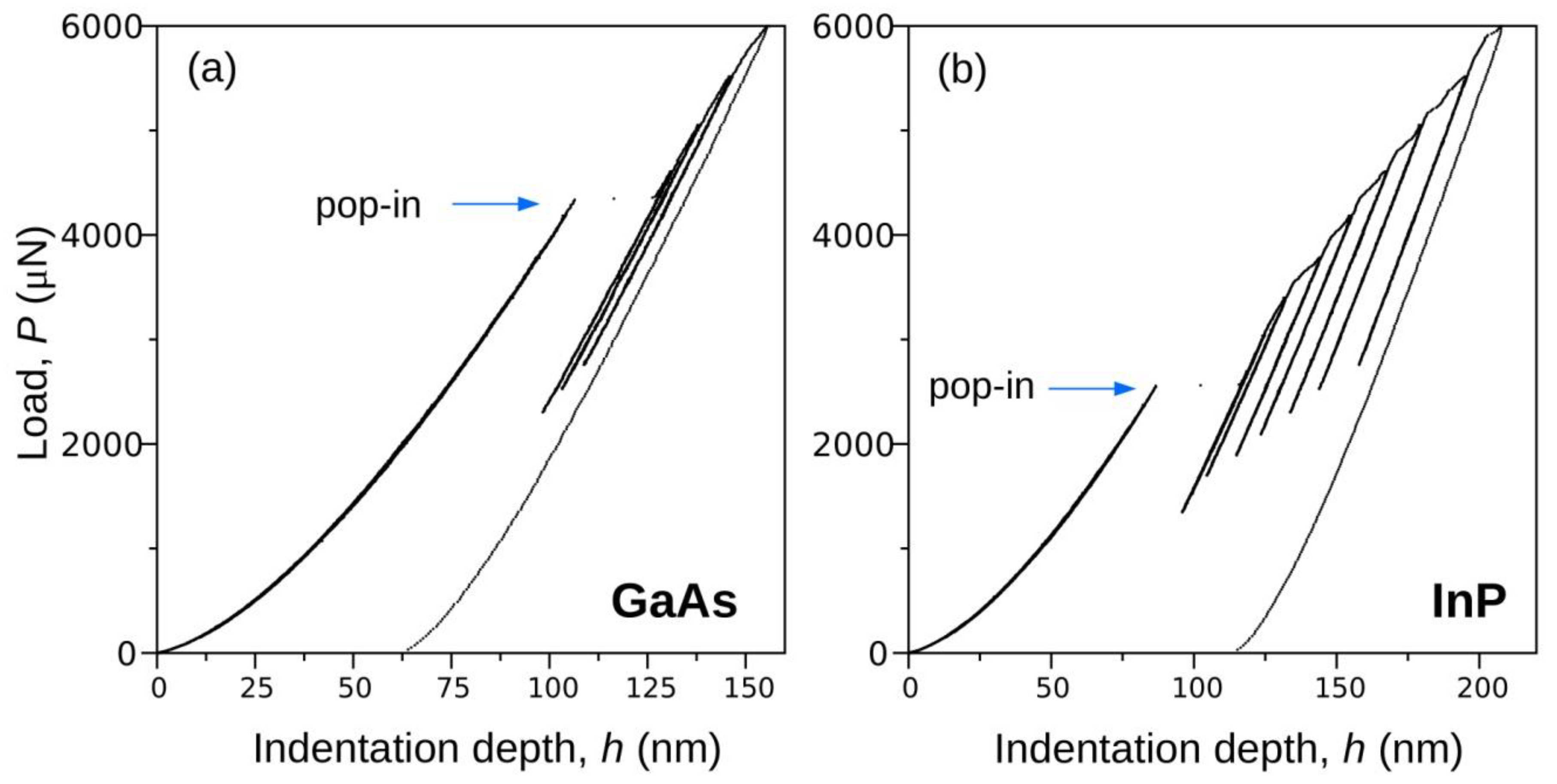
3.1. Nanoindentation Experiments

The results of nanointentation measurements (P-h curves) were analyzed within the framework of the Hertz theory, which relates to the contact of a rigid sphere with the flat surface of the isotropic body [20]. From an experimental point of view, our attention was focused on the relationship between load (P) and indenter displacement (h) given by the following equation:
P = 4 3 E r R 1 / 2 h 3 / 2
where Er is the reduced Young’s modulus: 1/Er = (1 − ν12)/E1 + (1 − ν22)/E2, ν is the Poisson ratio, E refers to the Young’s modulus, index 1 means the investigated material, while 2 indicates the indenter. Utilizing indentation curves registered for GaAs and based on its reduced Young’s modulus (Er = 87.2 GPa, E1 = 85.9 GPa, ν1 = 0.31, E2 = 1050 GPa, ν2 = 0.1 [21]), we fitted the Hertz formula (1) to the elastic part of the P-h curves (an example is presented in Figure 2a) and also estimated the indenter’s tip radius: R = 1178 ± 12 nm. Another important relationship derived from the Hertz theory concerns the radius of contact:
a = ( 3 P R 4 E r ) 1 / 3
Combining Equations (1) and (2), the formula describing the dependence of the contact pressure pc on the applied load can be obtained:
p c = P π a 2 = 2 3 ( 6 P E r 2 π 3 R 2 ) 1 / 3
The above equation was used to estimate the contact pressure at the pop-in event for all P-h curves measured for our GaAs and InP crystals.
Numerous nanoindentation (100) tests were performed for the GaAs crystal, which showed a systematic decrease in the pop-in load caused by an increase of the Si concentration (Figure 2a). Using Equation (3), we recalculated the recorded data to show that the mean contact pressure pm at the pop-in also exhibits similar behavior (refer to Table 1 and Figure 3a).
Analogous experiments (400 tests) and analysis were performed for the undoped, as well as for S- and Zn-doped InP crystals (Figure 2b). The final result is presented in Figure 3b, displaying an opposite effect to that obtained for GaAs, i.e., doping of InP causes an increase in the mean contact pressure at the beginning of the plastic deformation.
We limited our considerations to the first pop-in, which appears in the loading part of P–h curves and marks the onset of plastic deformation. In order to prove the last statement, we performed partial unloading experiments on undoped InP and GaAs crystals (see Figure 3). It can be seen that partial unloading carried out in the elastic range of deformation follows the path of the loading curve. In contrast, right after the first pop-in, the partial unloading leaves a “trace” different from that registered for loading.
An interesting result obtained for InP and GaAs crystals is the difference in the evolution of the plastic deformation, after the first pop-in. The P-h curves representing nanoindentation experiments performed for GaAs are smoother than the curves recorded for InP. In addition, the displacement of the indenter during plastic deformation is much larger in the case of an InP crystal. This result shows that nanoindentation stress promotes the development of the dislocation structure in the InP crystal more than in the case of GaAs.
The reduced Young’s modulus determined for GaAs crystals does not display substantial changes when doped with Si: Er(n1) = 87.3 ± 0.8 GPa, Er(n2) = 87.0 ± 0.4 GPa, Er(n3) = 86.7 ± 0.5 GPa. In contrast, our experiments on InP demonstrate the increase of Er value with Zn- or S-doping: Er(ud) = 62.5 ± 0.9 GPa, Er(S) = 68.6 ± 0.4 GPa, Er(Zn) = 67.3 ± 0.6 GPa (ud—undoped). It is worth noting that the Er values obtained for GaAs are close to the value calculated theoretically: 87.2 GPa. Similarly, the Er values obtained for InP are close to the theoretical value, 65.8 GPa [21]. These results confirm correctness of the applied experimental procedure.
In order to discuss the main results of our experiments, it should be recalled that the doping of GaAs by Si decreases the pressure (pPT) under which the phase transformation GaAs-I → GaAs-II occurs [22]. On the other hand, GaAs doping should increase the shear stress required for nucleation of dislocations [13,14]. Therefore, taking into account the results of nanoindentation experiments (see Figure 4a), it can be concluded that nanoindentation-induced plastic deformation in GaAs is initiated by phase transformation rather than nucleation of dislocations, which agrees with the previous reports [23,24].
In contrast, the analysis of experiments carried out for InP crystals (Figure 4b) reveals that the mean contact pressure of the pop-in event is higher for doped crystals. Since InP doping should increase the shear stress for nucleation of dislocations [15,16,17,18,19] and simultaneously decrease of the pressure of phase transformation [11,12], the conclusion can be formulated as follows: plasticity of the InP crystal induced by nanoindentation is initiated by the generation of dislocations.

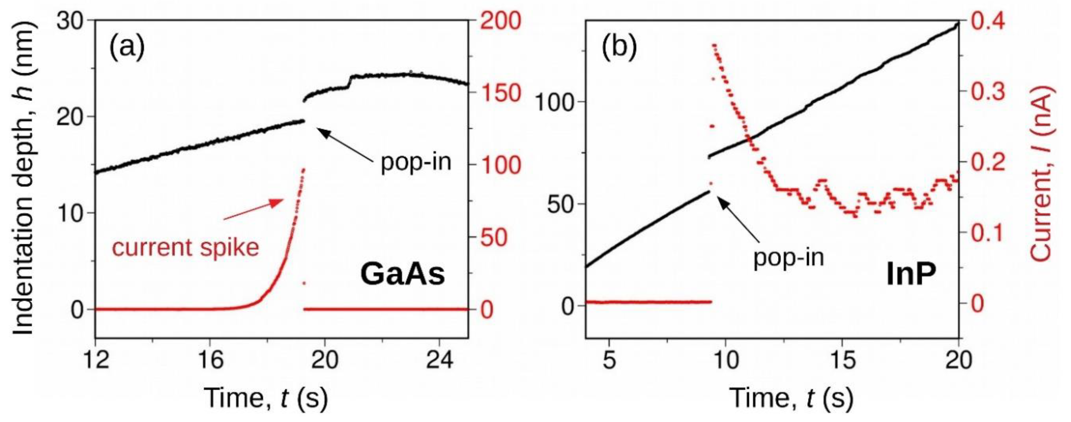
3.2. Nanoelectrical Experiments

Nanoelectrical measurements were carried out for Si-doped GaAs and InP crystals with a carrier concentration of 5.5 × 10¹⁶ and 1.0 × 10¹⁸, respectively. Thus, our experiments utilized n-type semiconductors. Because of the higher carrier mobility [21] displayed by GaAs, the best results for this crystal were obtained using the Berkovich conductive diamond indenter. However, measurements made for InP, which exhibit lower carrier mobility [21], used the spherical diamond indenter (R ≈ 1 μm) as it ensures the contact area greater than in the case of the Berkovich indenter. The conductive indenter and the sample surface form the metal–semiconductor junction that has been subjected to a reverse 3 V and 5 V voltage bias for GaAs and InP crystals, respectively. The results of the analysis are presented in the form of the h(t) and I(t) relationship, where I is the electric current and t is the nanoindentation time (Figure 5). It is worth noting that the results of nanoelectric measurements were reproducible; therefore, we present the only representative part of the performed measurements.
In the elastic range of deformation, the reverse voltage prevents the current from flowing through the contact between the conductive indenter with the surface of the GaAs sample (the Schottky contact) (Figure 5a). However, a leakage of the current through the Schottky barrier already begins in the range of the elastic deformation. Then, the current flow increases (still during elastic deformation) and suddenly reaches zero at the moment of the elastic–plastic transition. This characteristic connection between the electrical current and the indenter displacement suggests that the electrical (current spike) and mechanical (pop-in) peculiarities are of the same origin.
The sudden current drop that was observed at the onset of GaAs plastic deformation cannot be associated with the generation of dislocations. Indeed, it was shown earlier that an increase in silicon concentration reduces the contact pressure of the elastic–plastic transition in GaAs, which reveals the effect of phase transformation on this phenomenon. Given this, the presence of the current spike on the I(t) curve can be qualitatively explained. The metal–semiconductor junction under a reverse voltage stops the current. However, as the load applied to the conductive indenter increases, the junction begins to leak, which is displayed by an increasing electrical current. The observed effect is due to a decrease of the Schottky barrier, which is caused by non-homogeneous stress distribution in the vicinity of the contact area. Then, at the instant of the elastic–plastic transition, transformation to the high-pressure, metallic GaAs-II phase occurs. In this way, a new Schottky junction is established on the boundary between the semiconductor (GaAs-I) and metallic (GaAs-II) phases of GaAs, which is as a direct cause of the sudden drop of the electric current, which is clearly shown in Figure 5a.
A different effect was observed during nanoelectrical measurements carried out for the Si-doped InP crystal. Unlike the GaAs case, the process that initiates InP plasticity causes an increase in electrical current when the pop-in occurs (Figure 5b). This phenomenon can be explained with the aid of the results of nanoindentation experiments discussed above (refer to Figure 4b). Indeed, we came to the conclusion that the generation of dislocations is the cause of the incipient InP plasticity. Therefore, considering that the early stage of plastic deformation is characterized by a relatively low dislocation density, we suppose that this may result in an increase in the concentration of electrical current carriers, similarly to the silicon case described by Yakimov et al. [25]. This subtle effect caused by the generation of new donor states in the forbidden energy band gap seems to be a direct cause of the increase in electric current at the beginning of the elastic–plastic transition. It should be noted that an increase in the carrier concentration due to the presence of screw dislocations in the semiconductors’s lattice was also predicted theoretically [26] and the phenomenon was also observed in Si nanowires [27].
As far as the subsequent stages of plastic deformation are concerned (Figure 5b), we observed a marked decrease of the electric current, followed by fluctuations around 0.15 nA. Based on the available literature, we may attribute the registered current variations to the changes of contact area due to dislocation activity. Such a process (highly unpredictable) should cause small current fluctuations—similar to these disclosed by our experiments, clearly visible due to the low current value (~0.15 nA). Furthermore, an influence of dislocations on the current density remains a disputable issue. It is already known that an increase of resistivity stems from acceptor sites at semiconductor dangling bonds located along dislocations, which, in turn, results in the formation of charged regions that scatter electrons [28]. Moreover, high strains in a core of a dissociated dislocation modify the local band structure and result in highly conductive channels along the dislocation core [29].

4. Conclusions

In summary, this article presents nanoindentation-induced plasticity of a GaAs crystal as a phenomenon initiated by the GaAs-I → GaAs-II phase transformation. In contrast, plastic deformation in the InP crystal is initiated by the generation of dislocations. The above statements have been justified using nanoindentation experiments supported by nanoelectrical measurements on undoped and doped crystals. A noteworthy takeaway is that these experimental techniques may be used to study the initial stages of plastic deformation of other semiconductors as well as their nanoobjects, which seems to be important for the development and fabrication of optoelectronic as well as micro-electro-mechanical systems.

Author Contributions

Conceptualization, D.C.; investigation, D.C. and M.T.; writting—original draft preparation, D.C., A.C. and R.N.

Funding

This research was funded by the National Science Centre, Poland (Grant No. 2016/21/B/ST8/02737).

Acknowledgments

The authors acknowledge support from the CSC-IT Center for Science (Finland) for computational resources. RN and MT acknowledge the Department of Chemistry and Materials Science for overall support.

Conflicts of Interest

The authors declare no conflict of interest.

References

  1. Siwak, N.P.; Fan, X.Z.; Ghodssi, R. Fabrication challenges for indium phosphide microsystems. J. Micromech. Microeng. 2015, 25, 043001. [Google Scholar] [CrossRef]
  2. Corcoran, S.G.; Colton, R.J.; Lilleodden, E.T.; Gerberich, W.W. Anomalous plastic deformation at surfaces: Nanoindentation of gold single crystals. Phys. Rev. B 1997, 55, R16057. [Google Scholar] [CrossRef]
  3. Gerbig, Y.B.; Michaels, C.A.; Forster, A.M.; Cook, R.F. In situ observaation of the indentation-induced phase transformation of silicon thin films. Phys. Rev. B 2012, 85, 104102. [Google Scholar] [CrossRef] [Green Version]
  4. Jurkiewicz, K.; Pawlyta, M.; Zygadło, D.; Chrobak, D.; Duber, S.; Wrzalik, R.; Ratuszna, A.; Burian, A. Evolution of glassy carbon under heat treatment: Correlation structure–mechanical properties. J. Mater. Sci. 2018, 53, 3509–3523. [Google Scholar] [CrossRef] [Green Version]
  5. Schuh, C.A.; Mason, J.K.; Lund, A.C. Quantitative insight into dislocation nucleation from high-temperature nanoindentation experiments. Nat. Mater. 2005, 4, 617. [Google Scholar] [CrossRef] [PubMed]
  6. Szlufarska, I.; Nakano, A.; Vashista, P. A Crossover in the mechanical response of nanocrystalline ceramics. Science 2005, 309, 911–914. [Google Scholar] [CrossRef] [PubMed] [Green Version]
  7. Le Bourhis, E.; Patriarche, G. Structure of nanoindentations in heavily n- and p-doped (001) GaAs. Acta Mater. 2008, 56, 1417–1426. [Google Scholar] [CrossRef]
  8. Wasmer, K.; Gassilloud, R.; Michler, J.; Ballif, C. Analysis of onset of dislocation nucleation during nanoindentation and nanoscratching of InP. J. Mater. Res. 2012, 27, 320–329. [Google Scholar] [CrossRef] [Green Version]
  9. Jian, S.R.; Jang, J.S.C. Berkovich nanoindentation on InP. J. Alloy. Compd. 2009, 482, 498–501. [Google Scholar] [CrossRef]
  10. Chrobak, D.; Raisanen, J.; Nowak, R. Effect of silicon on the elastic–plastic transition of GaAs crystal. Scr. Mater. 2015, 102, 31–34. [Google Scholar] [CrossRef]
  11. Lin, C.M.; Hsu, I.J.; Lin, S.C.; Chuang, Y.C.; Juang, J.Y. Pressure effect on impurity local vibrational mode and phase transitions in n-type iron-doped indium phosphide. Sci. Rep. 2018, 8, 1284. [Google Scholar] [CrossRef] [PubMed] [Green Version]
  12. Bose, D.N.; Seishu, B.; Parthasarathy, G.; Gopal, E.S.R. Doping dependence of semiconductor-metal transitionin InP at high pressures. Proc. R. Soc. Lond. A Math. Phys. Sci. 1986, 405, 345–353. [Google Scholar] [CrossRef]
  13. Bourret, E.D.; Tabache, M.G.; Beeman, J.W.; Elliot, A.G.; Scott, M. Silicon and indium doping of GaAs: Measurements of the effect of doping on mechanical behavior and relation with dislocation formation. J. Cryst. Growth 1987, 85, 275–281. [Google Scholar] [CrossRef] [Green Version]
  14. Djemel, A.; Castaing, J.; Burle-Durbec, N.; Pichaud, B. Dislocation multiplication in GaAs: Inhibition by doping. Revue de Physique Appliquée 1989, 24, 779–793. [Google Scholar] [CrossRef] [Green Version]
  15. Arivuoli, D.; Fornari, R.; Kumar, J. Microhardness studies of doped and undoped InP crystals. J. Mater. Sci. Lett. 1991, 10, 559–561. [Google Scholar] [CrossRef]
  16. Brasen, D.; Bonner, W.A. Effect of temperature and sulfur doping on the plastic deformation of InP single crystals. Mater. Sci. Eng. 1983, 61, 167–172. [Google Scholar] [CrossRef]
  17. Yonenaga, I.; Sumino, K. Effects of dopants on dynamic behavior of dislocations and mechanical strength in InP. J. Appl. Phys. 1993, 74, 917–924. [Google Scholar] [CrossRef]
  18. Roksnoer, P.J.; van Rijbroek-van den Boom, M.M.B. The single crystal growth and characterization of indium phosphide. J. Cryst. Growth 1984, 66, 317–326. [Google Scholar] [CrossRef]
  19. Oda, O.; Katagiri, K.; Shinohara, K.; Katsura, S.; Takahashi, Y.; Kainosho, K.; Kohiro, K.; Hirano, R. InP crystal growth. Substrate preparation and evaluation. Semicond. Semimet. 1990, 31, 93–174. [Google Scholar]
  20. Johnson, K.L. Contact Mechanics, 1st ed.; Cambridge University Press: Cambridge, UK, 1985; pp. 85–95. [Google Scholar]
  21. Semiconductors on NSM. Available online: www.ioffe.ru/SVA/NSM/Semicond/ (accessed on 26 October 2019).
  22. Mujica, A.; Rubio, A.; Munoz, A.; Needs, R.J. High-pressure phases of group-IV, III–V, and II–VI compounds. Rev. Mod. Phys. 2003, 75, 863. [Google Scholar] [CrossRef] [Green Version]
  23. Chrobak, D.; Nordlund, K.; Nowak, R. Nondislocation origin of gaas nanoindentation pop-in event. Phys. Rev. Lett. 2007, 98, 045502. [Google Scholar] [CrossRef] [PubMed]
  24. Nowak, R.; Chrobak, D.; Nagao, S.; Vodnick, D.; Berg, M.; Tukiainen, A.; Pessa, M. An electric current spike linked to nanoscale plasticity. Nat. Nanotechnol. 2009, 4, 287. [Google Scholar] [CrossRef] [PubMed]
  25. Yakimov, E. Dislocation-point defect interaction effect on local electrical properties of semiconductors. J. de Physique III 1997, 7, 2293. [Google Scholar] [CrossRef]
  26. Bakke, K.; Moraes, F. Threading dislocation densities in semiconductor crystals: A geometric approach. Phys. Lett. A 2012, 376, 2838–2841. [Google Scholar] [CrossRef] [Green Version]
  27. Qader, I.N.; Omar, M.S. Carrier concentration effect and other structure-related parameters on lattice thermal conductivity of Si nanowires. Bull. Mater. Sci. 2017, 40, 599–607. [Google Scholar] [CrossRef]
  28. Broudy, R.M. The electrical properties of dislocations in semiconductors. Adv. Phys. 1963, 12, 135–184. [Google Scholar] [CrossRef]
  29. Reiche, M.; Kittler, M.; Erfurth, W.; Pippel, E.; Sklarek, K.; Blumtritt, H.; Haehnel, A.; Uebensee, H. On the electronic properties of a single dislocation. J. Appl. Phys. 2014, 115, 194303. [Google Scholar] [CrossRef] [Green Version]
Figure 1. Schematic of the experimental setup used for nanoindentation and nanoECR experiments.
Crystals 09 00651 g001
Figure 2. Results of nanomechanical experiments. The P–h curves exhibit characteristic discontinuities marked by arrows. (a) The nanoindentation curves collected for doped GaAs crystals display a decrease of the load at the beginning of plastic deformation (pop-in) caused by an increase of Si concentration (n1 < n2 < n3, refer to Table 1). (b) In contrast, the nanoindentation curves measured for undoped and doped InP crystal show an increase of the load at the beginning of plastic deformation caused by doping.
Crystals 09 00651 g002
Figure 3. Results of partial unloading experiments performed for GaAs (a) and InP (b) crystals. The first pop-in marks the onset of plastic deformation.
Crystals 09 00651 g003
Figure 4. Results of nanoindentation experiments that show an effect of doping on the mean contact pressure (pm) at the onset of plastic deformation. (a) An increase of Si concentration (n1 < n2 < n3, refer to Table 1) causes a decrease of pm. The value of pm read 13.7 ± 0.4, 13.3 ± 0.2 and 12.6 ± 0.4 GPa for n1, n2 and n3 silicon concentration, respectively. (b) An opposite effect was registered for InP crystals. The value of pm read 7.6 ± 0.4, 8.2 ± 0.3 and 8.0 ± 0.4 GPa for undoped, S-doped and Zn-doped crystal, respectively.
Crystals 09 00651 g004
Figure 5. Results of nanoECR experiments registered for GaAs and InP crystal. (a) The I(t) curve obtained for GaAs exhibit the current spike at the beginning of the elastic–plastic transition. (b) In contrast, the nanoECR curve of InP shows sudden increase of the current at the pop-in event.
Crystals 09 00651 g005
Table 1. The carrier concentration (n) and the pop-in mean contact pressure (pm) measured for GaAs and InP crystals.
(001) GaAs, Si Doped(001) InP
n1n2n3UndopedS-DopedZn-Doped
n (cm−3)5.5 × 10163.1 × 10172.6 × 10185.1 × 10151.8 × 10183.2 × 1018
pm (GPa)13.7 ± 0.4 13.3 ± 0.212.6 ± 0.47.6 ± 0.48.2 ± 0.38.0 ± 0.4

