
Dependence of GaN Exciton Energy on Temperature


 , ,
, ,  and
and
Abstract
1. Introduction
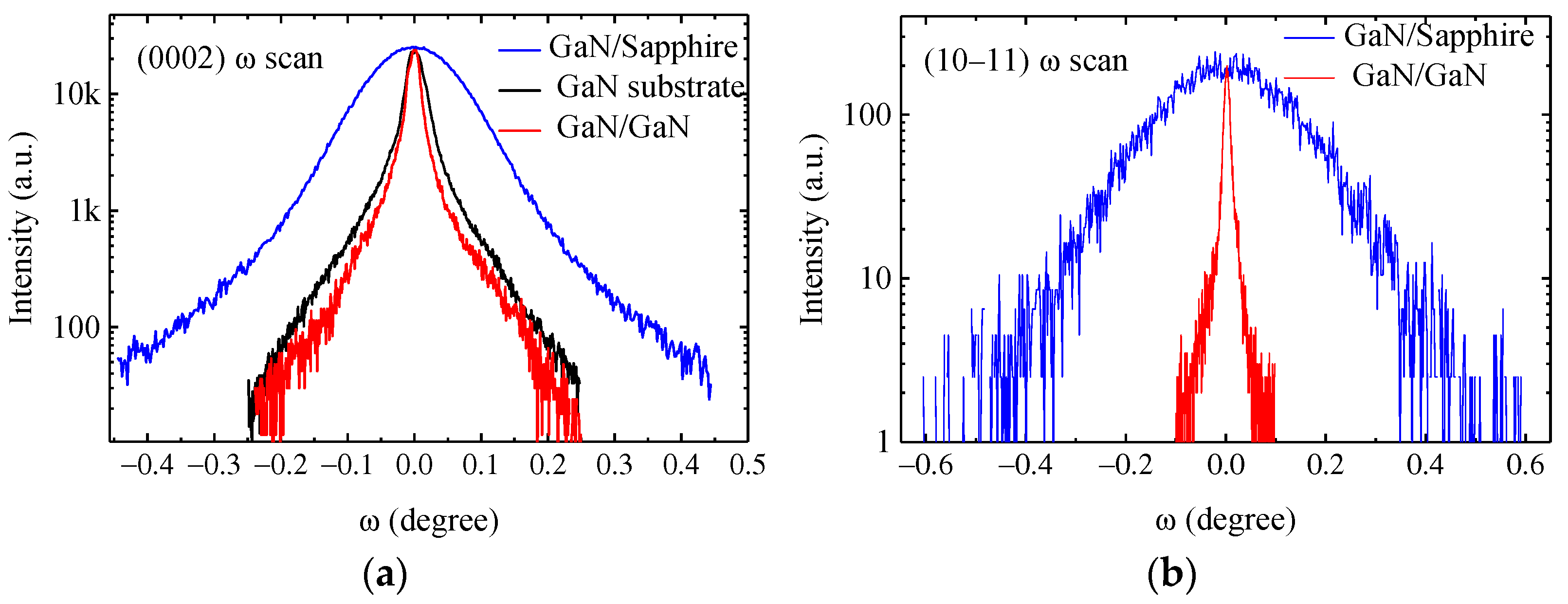
2. Experiments
3. Calculations and Models
3.1. Early Models
3.1.1. Varshni’s Model
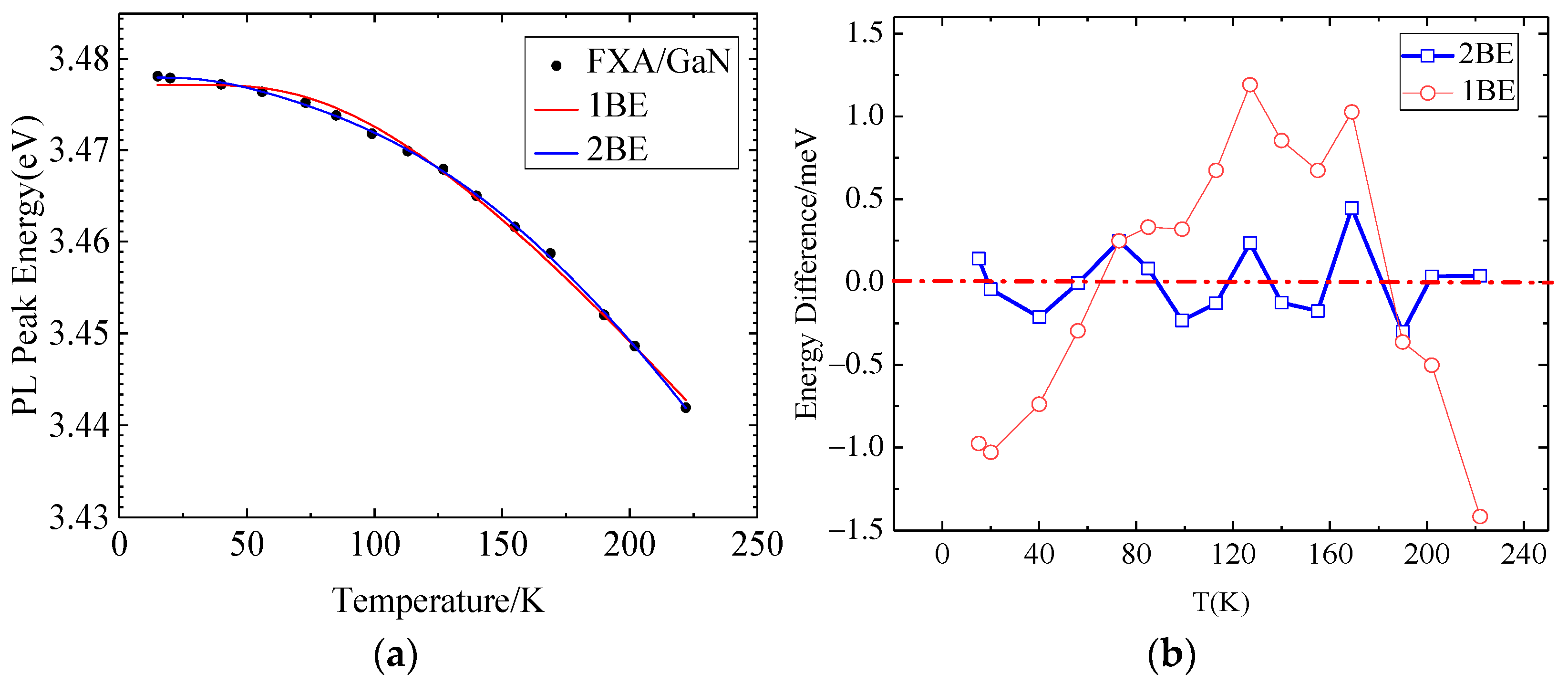
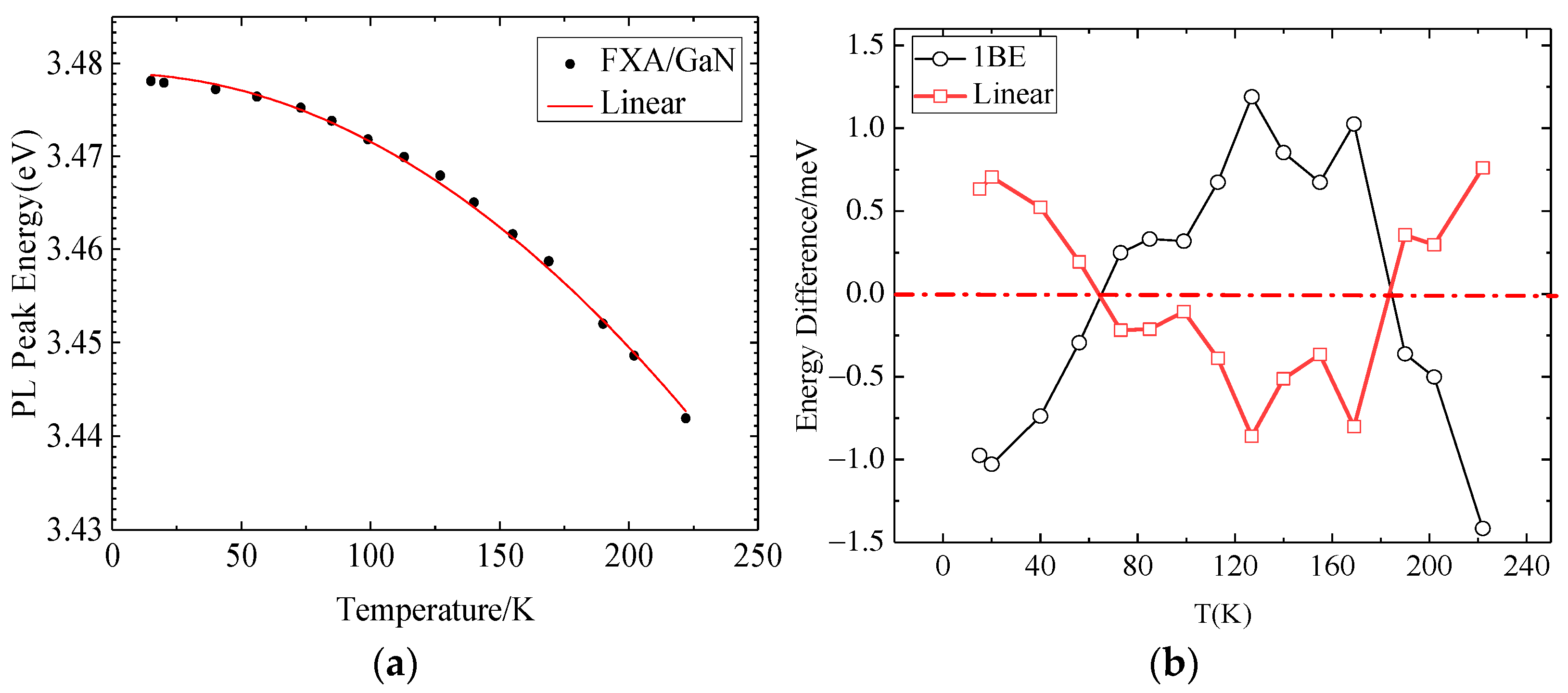
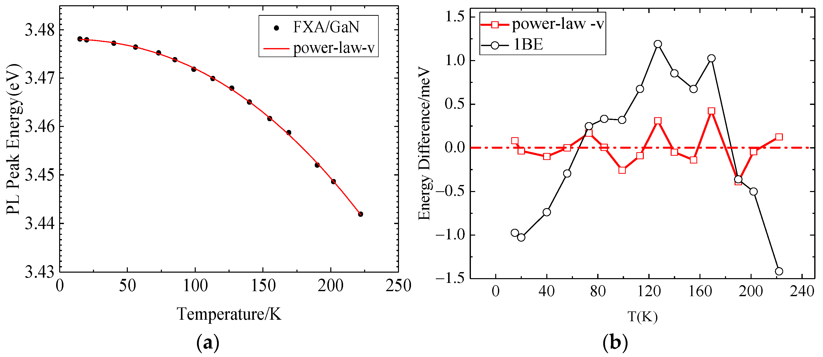
3.1.2. Bose–Einstein Model (1BE Model)
3.2. Novel Model
3.2.1. Singular Model (2BE Model)
3.2.2. Linear Model
3.2.3. Power-Law Model
- (a)
- Power-law-delta model
- (b)
- Power-law-v model
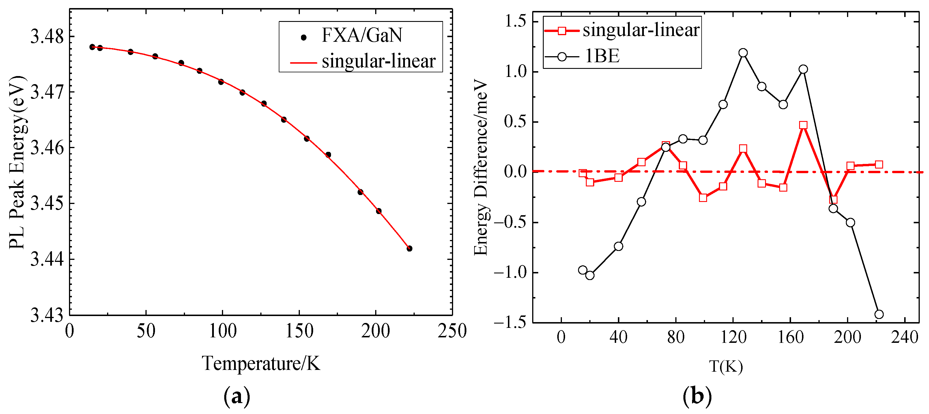
3.2.4. Singular-Linear Model
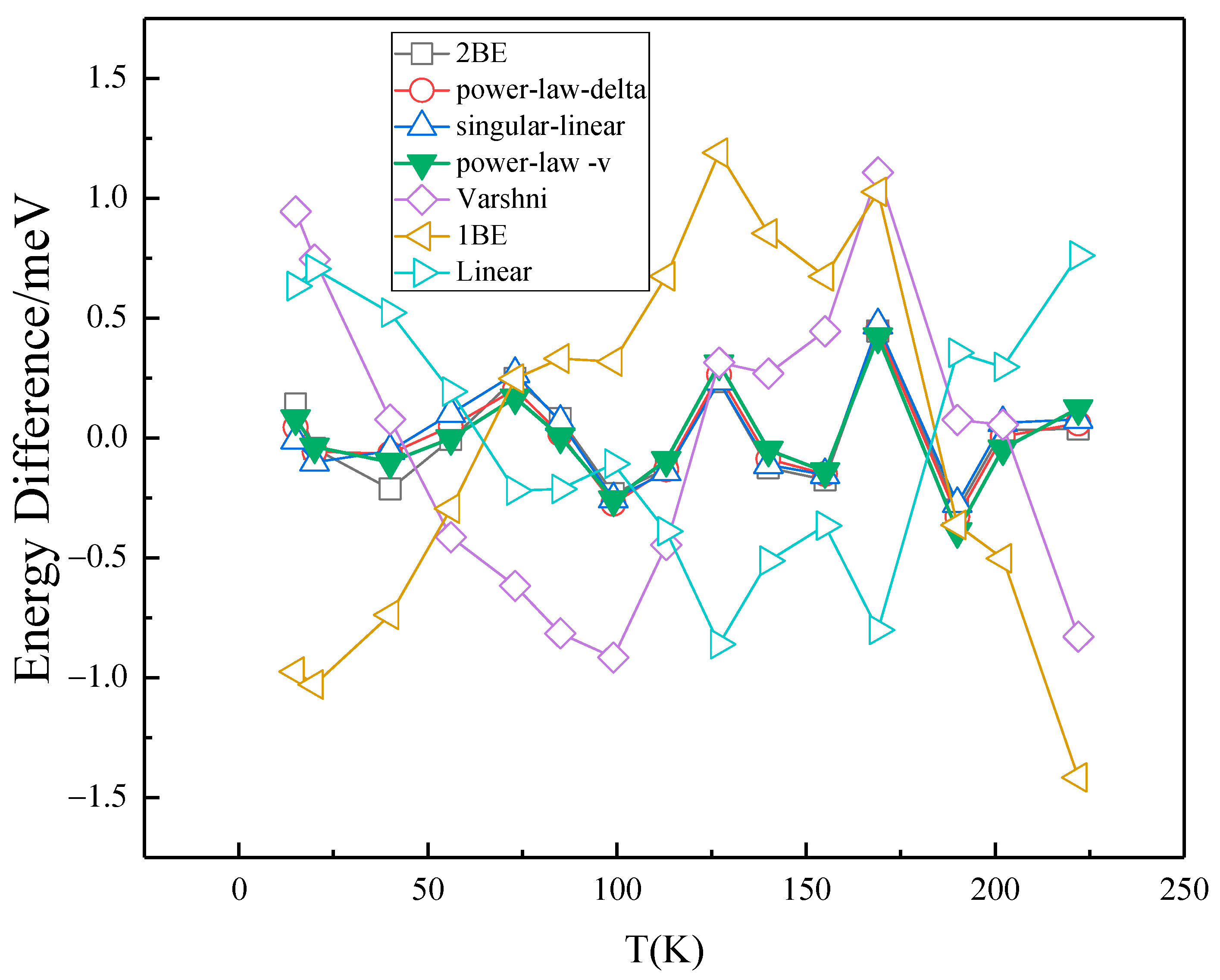
4. Discussion
5. Conclusions
Author Contributions
Funding
Data Availability Statement
Acknowledgments
Conflicts of Interest
References
- Boutramine, A. Temperature-and Composition-Dependent Band Gap Energy and Electron–Phonon Coupling in InAs1−xSbx Semiconductors Alloys for Infrared Photodetection. J. Electron. Mater. 2023, 52, 6031–6041. [Google Scholar] [CrossRef]
- Isik, M.; Gasanly, N.M.; Darvishov, N.H.; Bagiev, V.E. Effect of temperature on band gap of PbWo4 single crystals grown by Czochralski method. Phys. Scr. 2022, 97, 45803. [Google Scholar] [CrossRef]
- Kumar, A.; Kumar, S.; Miyai, Y.; Shimada, K. Temperature-dependent band modification and energy dependence of the electron-phonon interaction in the topological surface state on Bi2Te3. Phys. Rev. B 2022, 106, 121104. [Google Scholar] [CrossRef]
- Surucu, O.; Isik, M.; Terlemezoglu, M.; Bektas, T.; Gasanly, N.M.; Parlak, M. Temperature effects on optical characteristics of thermally evaporated CuSbSe2 thin films for solar cell applications. Opt. Mater. 2022, 133, 113047. [Google Scholar] [CrossRef]
- Wu, R.; Ma, M.; Zhang, S.; Zhao, P.; Li, K.; Zhao, Q.; Chang, A.; Zhang, B. Enhanced linearity of CaCu3Ti4O12 by changing energy band structure induced by Fe3+ doping for high temperature thermistor application. Appl. Phys. Lett. 2022, 121, 96124. [Google Scholar] [CrossRef]
- Tamariz, S.; Callsen, G.; Stachurski, J.; Shojiki, K.; Butté, R.; Grandjean, N. Toward Bright and Pure Single Photon Emitters at 300 K Based on GaN Quantum Dots on Silicon. ACS Photonics 2020, 7, 1515–1522. [Google Scholar] [CrossRef]
- Deng, J.; Yu, J.; Hao, Z.; Kang, J.; Lu, B.; Wang, L.; Sun, C.; Han, Y.; Xiong, B.; Wang, J.; et al. Disk-Shaped GaN Quantum Dots Embedded in AlN Nanowires for Room-Temperature Single-Photon Emitters Applicable to Quantum Information Technology. ACS Appl. Nano Mater. 2022, 5, 4000–4008. [Google Scholar] [CrossRef]
- Allen, P.B.; Cardona, M. Temperature dependence of the direct gap of Si and Ge. Phys. Rev. B 1983, 27, 4760–4769. [Google Scholar] [CrossRef]
- Hartel, A.M.; Gutsch, S.; Hiller, D.; Zacharias, M. Fundamental temperature-dependent properties of the Si nanocrystal band gap. Phys. Rev. B 2012, 85, 165306. [Google Scholar] [CrossRef]
- Klenner, M.; Falter, C.; Ludwig, W. Temperature dependence of band gaps in Si and Ge in the quasiion model. Ann. Phys. 2006, 504, 34–38. [Google Scholar] [CrossRef]
- Lautenschlager, P.; Allen, P.B.; Cardona, M. Temperature dependence of band gaps in Si and Ge. Phys. Rev. B 1985, 31, 2163–2171. [Google Scholar] [CrossRef] [PubMed]
- Vainorius, N.; Kubitza, S.; Lehmann, S.; Samuelson, L.; Dick, K.A.; Pistol, M.-E. Temperature dependent electronic band structure of wurtzite GaAs nanowires. Nanoscale 2018, 10, 1481–1486. [Google Scholar] [CrossRef] [PubMed]
- Pavesi, L.; Piazza, F.; Rudra, A.; Carlin, J.F.; Ilegems, M. Temperature dependence of the InP band gap from a photoluminescence study. Phys. Rev. B 1991, 44, 9052–9055. [Google Scholar] [CrossRef]
- Rong, X.; Lu, Y.; Yin, J.; Jiang, H.; Han, S.; Zeng, Y.; Xu, W.; Fang, M.; Cao, P.; Zhu, D.; et al. Electroluminescence enhancement of ZnO nanorod array/GaN heterojunction with MgZnO barrier layer. J. Lumin. 2022, 248, 118946. [Google Scholar] [CrossRef]
- Xu, R.; Chen, P.; Zhou, J.; Li, Y.; Li, Y.; Zhu, T.; Cheng, K.; Chen, D.; Xie, Z.; Ye, J.; et al. High Power Figure-of-Merit, 10.6-kV AlGaN/GaN Lateral Schottky Barrier Diode with Single Channel and Sub-100-µm Anode-to-Cathode Spacing. Small 2022, 18, e2107301. [Google Scholar] [CrossRef]
- Xu, R.; Chen, P.; Liu, M.H.; Zhou, J.; Yang, Y.F.; Li, Y.M.; Ge, C.; Peng, H.C.; Liu, B.; Chen, D.J.; et al. 1.4-kV Quasi-Vertical GaN Schottky Barrier Diode With Reverse Junction Termination. IEEE J. Electron Devices Soc. 2020, 8, 316–320. [Google Scholar] [CrossRef]
- Xu, R.; Chen, P.; Liu, M.H.; Zhou, J.; Li, Y.M.; Liu, B.; Chen, D.J.; Xie, Z.L.; Zhang, R.; Zheng, Y.D. 2.7-kV AlGaN/GaN Schottky barrier diode on silicon substrate with recessed-anode structure. Solid-State Electron. 2021, 175, 107953. [Google Scholar] [CrossRef]
- Patra, S.K.; Schulz, S. Exploring the Potential of c-Plane Indium Gallium Nitride Quantum Dots for Twin-Photon Emission. Nano Lett. 2020, 20, 234–241. [Google Scholar] [CrossRef]
- Delphan, A.; Makhonin, M.N.; Isoniemi, T.; Walker, P.M.; Skolnick, M.S.; Krizhanovskii, D.N.; Skryabin, D.V.; Carlin, J.-F.; Grandjean, N.; Butté, R. Polariton lasing in AlGaN microring with GaN/AlGaN quantum wells. APL Photonics 2023, 8, 021302. [Google Scholar] [CrossRef]
- Yang, J.; Tao, R.; Huang, Z.; Li, D.; Rong, X.; Chu, Z.; Liu, Q.; Huo, X.; Li, T.; Sheng, B.; et al. A near-resonant excitation strategy to achieve ultra-low threshold GaN polariton lasing. Opt. Lett. 2024, 49, 4058–4061. [Google Scholar] [CrossRef]
- Xu, R.; Chen, P.; Liu, M.H.; Zhou, J.; Li, Y.M.; Cheng, K.; Liu, B.; Chen, D.J.; Xie, Z.L.; Zhang, R.; et al. 3.4-kV AlGaN/GaN Schottky Barrier Diode on Silicon Substrate With Engineered Anode Structure. IEEE Electron Device Lett. 2021, 42, 208–211. [Google Scholar] [CrossRef]
- Xu, R.; Chen, P.; Liu, X.; Zhao, J.; Zhu, T.; Chen, D.; Xie, Z.; Ye, J.; Xiu, X.; Wan, F.; et al. A lateral AlGaN/GaN Schottky barrier diode with 0.36-V turn-on voltage and 10-kV breakdown voltage by using double-barrier anode structure. Chip 2024, 3, 100079. [Google Scholar] [CrossRef]
- Vasileff, H.D. Electron Self-Energy and Temperature-Dependent Effective Masses in Semiconductors:n-Type Ge and Si. Phys. Rev. 1957, 105, 441–446. [Google Scholar] [CrossRef]
- Pssler, R. Basic Model Relations for Temperature Dependencies of Fundamental Energy Gaps in Semiconductors. Phys. Status Solidi B 1997, 200, 155–172. [Google Scholar] [CrossRef]
- Uesugi, K.; Suemune, I.; Hasegawa, T.; Akutagawa, T.; Nakamura, T. Temperature dependence of band gap energies of GaAsN alloys. Appl. Phys. Lett. 2000, 76, 1285–1287. [Google Scholar] [CrossRef]
- Pässler, R. Temperature dependence of fundamental band gaps in group IV, III–V, and II–VI materials via a two-oscillator model. J. Appl. Phys. 2001, 89, 6235–6240. [Google Scholar] [CrossRef]
- Zardas, G.E.; Yannakopoulos, P.H.; Ziska, M.; Symeonides, C.; Vesely, M.; Euthymiou, P.C. Temperature dependence of Si–GaAs energy gap using photoconductivity spectra. Microelectron. J. 2006, 37, 91–93. [Google Scholar] [CrossRef]
- Pässler, R. Temperature dependence of exciton peak energies in multiple quantum wells. J. Appl. Phys. 1998, 83, 3356–3359. [Google Scholar] [CrossRef]
- Liu, R.; Bayram, C. Cathodoluminescence study of luminescence centers in hexagonal and cubic phase GaN hetero-integrated on Si(100). J. Appl. Phys. 2016, 120, 025106. [Google Scholar] [CrossRef]
- Na, J.H.; Taylor, R.A.; Rice, J.H.; Robinson, J.W.; Lee, K.H.; Park, Y.S.; Park, C.M.; Kang, T.W. Two-dimensional exciton behavior in GaN nanocolumns grown by molecular-beam epitaxy. Appl. Phys. Lett. 2005, 86, 123102. [Google Scholar] [CrossRef]
- Viswanath, A.K.; Lee, J.I.; Yu, S.; Kim, D.; Choi, Y.; Hong, C.-h. Photoluminescence studies of excitonic transitions in GaN epitaxial layers. J. Appl. Phys. 1998, 84, 3848–3859. [Google Scholar] [CrossRef]
- Zhang, W.; Growden, T.A.; Berger, P.R.; Storm, D.F.; Meyer, D.J.; Brown, E.R. Temperature Characterization of Unipolar-Doped Electroluminescence in Vertical GaN/AlN Heterostructures. Energies 2021, 14, 6654. [Google Scholar] [CrossRef]
- Cretì, A.; Tobaldi, D.M.; Lomascolo, M.; Tarantini, I.; Esposito, M.; Passaseo, A.; Tasco, V. Exciton Effects in Low-Barrier GaN/AlGaN Quantum Wells. J. Phys. Chem. C 2022, 126, 14727–14734. [Google Scholar] [CrossRef]
- Boughrara, N.; Benzarti, Z.; Khalfallah, A.; Evaristo, M.; Cavaleiro, A. Comparative study on the nanomechanical behavior and physical properties influenced by the epitaxial growth mechanisms of GaN thin films. Appl. Surf. Sci. 2022, 579, 152188. [Google Scholar] [CrossRef]
- Viña, L.; Logothetidis, S.; Cardona, M. Temperature dependence of the dielectric function of germanium. Phys. Rev. B 1984, 30, 1979–1991. [Google Scholar] [CrossRef]
- Pässler, R. Alternative analytical descriptions of the temperature dependence of the energy gap in cadmium sulfide. Phys. Status Solidi B 2006, 193, 135–144. [Google Scholar] [CrossRef]
- Collins, A.T.; Lawson, S.C.; Davies, G.; Kanda, H. Indirect Energy Gap of 13C Diamond. Phys. Rev. Lett. 1990, 65, 891. [Google Scholar] [CrossRef]
- O’Donnell, K.P.; Chen, X. Temperature dependence of semiconductor band gaps. Appl. Phys. Lett. 1991, 58, 2924–2926. [Google Scholar] [CrossRef]


| Equation | |||||||
|---|---|---|---|---|---|---|---|
| (1) | 3.4789 | 19 | 2509 | 216.2 | 0.996 | ||
| (2) | 3.47716 | 3.52 | 325.94 | 27.99 | 0.993 | ||
| (4) | 3.47779 | 5.7 | 138 | 645 | 0.211 | 0.9995 | |
| (6) | 3.478 | 5.7 | 478.96 | 0.46559 | 41.238 | 0.9997 | |
| (7) | 3.47809 | 18 | 1581 | 2.24 | 136.124 | 0.9996 | |
| (8) | 3.47825 | 5.8 | 711 | 0.465 | 0.9996 |
Disclaimer/Publisher’s Note: The statements, opinions and data contained in all publications are solely those of the individual author(s) and contributor(s) and not of MDPI and/or the editor(s). MDPI and/or the editor(s) disclaim responsibility for any injury to people or property resulting from any ideas, methods, instructions or products referred to in the content. |
© 2025 by the authors. Licensee MDPI, Basel, Switzerland. This article is an open access article distributed under the terms and conditions of the Creative Commons Attribution (CC BY) license (https://creativecommons.org/licenses/by/4.0/).
Share and Cite
Liu, X.; Chen, P.; Xie, Z.; Xiu, X.; Chen, D.; Zhao, H.; Shi, Y.; Zhang, R.; Zheng, Y. Dependence of GaN Exciton Energy on Temperature. Crystals 2025, 15, 137. https://doi.org/10.3390/cryst15020137
Liu X, Chen P, Xie Z, Xiu X, Chen D, Zhao H, Shi Y, Zhang R, Zheng Y. Dependence of GaN Exciton Energy on Temperature. Crystals. 2025; 15(2):137. https://doi.org/10.3390/cryst15020137
Chicago/Turabian StyleLiu, Xiancheng, Peng Chen, Zili Xie, Xiangqian Xiu, Dunjun Chen, Hong Zhao, Yi Shi, Rong Zhang, and Youdou Zheng. 2025. "Dependence of GaN Exciton Energy on Temperature" Crystals 15, no. 2: 137. https://doi.org/10.3390/cryst15020137
APA StyleLiu, X., Chen, P., Xie, Z., Xiu, X., Chen, D., Zhao, H., Shi, Y., Zhang, R., & Zheng, Y. (2025). Dependence of GaN Exciton Energy on Temperature. Crystals, 15(2), 137. https://doi.org/10.3390/cryst15020137