You are currently viewing a new version of our website. To view the old version click .
Crystals
  • Article
  • Open Access

15 February 2023

Investigation of the Temperature Dependence of Volt-Ampere Characteristics of a Thin-Film Si3N4 Memristor

,
,
,
,
and
1
Laboratory for the Study of Neuromorphic Systems, Joint-Stock Company Molecular Electronics Research Institute, 124460 Moscow, Russia
2
Industrial Artificial Intelligence, Artificial Intelligence Research Institute, 105064 Moscow, Russia
3
Research Center in Artificial Intelligence in the Direction of Optimization of Management Decisions to Reduce Carbon Footprint, Skolkovo Institute of Science and Technology, 121205 Moscow, Russia
*
Author to whom correspondence should be addressed.
This article belongs to the Special Issue Semiconductor Materials and Devices

Abstract

The compatibility of memristor materials with advanced complementary metal-oxide-semiconductor (CMOS) technology is a key factor for microelectronics element base manufacturing. Therefore, we continued studying previously fabricated CMOS-compatible Ni/Si3N4/SiO2/p+-Si samples. We approximated volt-ampere characteristics (VAC) at different temperatures using the general form of the spatial charge-limiting current (SCLC) equation assuming exponential and Gaussian trap distribution within the band gap of Si3N4. Our approximation demonstrated better experimental data matching compared to previous work, where the approximation was based on the uniform trap distribution law. Further, we performed another additional sample measurement set of the samples to evaluate the parameters of the low-resistance state (LRS) variations at different temperatures. Analysis of these measurements allowed us to estimate the temperatures at which the samples will retain LRS for 10 years.

1. Introduction

Modern and widely used computing devices are based on von Neumann architectures. They have a fundamental rate limitation for data transfer between dynamic random-access memory (DRAM) and the central processing unit (CPU) or its coprocessors. The CPU and memory are mostly fabricated using the CMOS process, which is the basis of the entire microelectronics industry. To eliminate this limitation related to external DRAM, new approaches propose to relocate computations from the entire CPU directly into the memory array in order to eliminate extra data pass. The most advanced of them are in-memory computing architectures, where input data are loaded, transformed, and stored in the same memory array. Such architectures use a non-volatile ultra-high-speed element base built on new principles—ReRAM (Resistive RAM), FRAM (Ferroelectric RAM), PCRAM (Phase change RAM), and others [1,2].
The memristor is considered one of the most efficient devices for in-memory computing. It was predicted by Leon Chua in 1971 [3] and was first implemented by Hewlett Packard in 2008 [4]. It typically consists of top and bottom electrodes separated by a dielectric. In a modern interpretation [5,6], the memristive effect refers to cyclic and reversible transitions between a high-resistance state (HRS) and a LRS. Such transitions occur under the influence of both a short voltage pulse and a smooth voltage change from one range boundary to another.
Limitations of memristors are caused by the complexity of simultaneously obtaining minimum acceptable values for all consumer parameters, including stability of the resistive state in time (retention), the durability of the number of switches (endurance), bit depth, and accuracy of their setting (plasticity), and parameters of pulse duration and amplitude during reading/writing [7,8].
Various physical effects can explain retention in memristors. When an electric field is applied to a dielectric, positive and negative charges shift. One of the mechanisms for the accumulation of such charges is various impurities. Depending on the dielectric material, its band gap may contain a set of energy levels where the charge carriers are trapped. Such trapping is due to the presence of impurities in a particular dielectric material. The further from the bottom of the conduction level the trapped carriers are, the higher activation energy is necessary for their release. Traps with energy levels located more than 1 eV below the bottom of the conduction zone are considered deep traps [9].
Therefore, impurities with deep energy levels significantly affect the concentration of trapped charge carriers, hence the operational characteristics of the memristor. These include the VAC and the HRS or LRS retention times. Determining the parameters of captured charge carriers’ distribution of energy levels allows for estimating their actual concentration. Thus, the characterization of impurities with deep energy levels is a necessary technological task.
Since the beginning of the 20th century, scientists have been developing and studying various models of the charge transfer mechanism for dielectrics, and then for memristors [5,10,11,12,13,14]. Some of the prominent models are the Frenkel model, the Schottky model, the Hill–Adachi model, the Makram–Ebeid and Lanno models, the Nasyrov–Gritsenko model, the SCLC model, and others.
In our work, we further studied the behavior of a sandwich structure with Ni as the top electrode and a bilayer dielectric of Si3N4 and SiO2 placed on a p-type silicon substrate. This structure was designed as a part of the study [13]. In [15], co-authors of this paper investigated the endurance of such structures and estimated it to be in the range of 5000–7000 resistive switching.
We noticed that in [13] some of the structural parameters obtained from the electrical response model are inconsistent. Therefore, we reviewed the electrical response model considering different trap distribution laws in the band gap. Then, we evaluated the stability of the resistive state over time. We reviewed the previously described electrical response model for Ni/Si3N4/SiO2/p+-Si structure and proposed a new approximation model using the SCLC equation with the Gaussian distribution of traps.
The contributions of this work are as follows:
  • We reviewed the previously described electrical response model for Ni/Si3N4/SiO2/p+-Si structure and proposed a new approximation model using the SCLC equation with a Gaussian distribution of trap states;
  • Using the mean absolute percentage error (MAPE) algorithm, we showed that the new approximation model provides a better experimental data fit;
  • We calculated and analyzed the Gaussian distribution of trap states at different temperatures for the LRS and HRS of the studied structure;
  • We measured memristor resistance over time at different elevated operating temperatures and evaluated conditions for 10-year LRS retention.
The paper content is organized as below. The Section 2 briefly provides the related research on the SCLC model, laws of distribution of trap states, and operation-specific memristors. The Section 3 includes a brief description of the fabricated structure. Then, the parameters of the SCLC model and expressions for the exponential and Gaussian law of trap distribution in the band gap were provided. To estimate the retention time of the LRS, Arrhenius’s law was chosen, and the temperature-dependent LRS resistance variation with time was determined. The Section 4 includes the approximation of VAC with consideration of the exponential and Gaussian law of trap distribution in the LRS and HRS of the memristor. An estimation of temperature conditions for LRS retention over 10 years was conducted as well. Finally, the Section 5 summarizes our research and includes an idea for further investigation.

3. Materials and Methods

3.1. Fabrication of the Ni/Si3N4/SiO2/p+-Si Structure

The Ni/Si3N4/SiO2/p+-Si structure considered in this paper was presented earlier in the article [13] (Figure 2). With the consent of all authors, we used their data for further analysis and samples for additional measurements. Below is the summary of the structure fabrication process.
Figure 2. Photo of the manufactured samples and their sketches.
A silicon p-type substrate with a resistivity of 0.005 Ohm⋅cm was used. Then, a 2 nm thick SiO2 layer was formed by thermal oxidation. Next, a 4 nm thick Si3N4 film was formed by low-pressure chemical vapor deposition (LPCVD) with a mixture of dichlorosilane (SiH2Cl2) and ammonia (NH3) in a ratio of 1:3 and at 700 °C.
A highly doped p+-type layer was formed in a silicon substrate. First, ion implantation with heavy boron difluoride BF2+ ions with an energy of 40 keV and a dose of 8 × 1014 cm−2 through the previously obtained dielectric layers was performed. Then, the impurity was activated by rapid thermal anneal performed at 1030 °C. Finally, the top Ni electrodes were deposited using a thermal evaporator through a shadow mask.

3.2. The SCLC Model and Laws of Trap Distribution for the VAC Approximation

In [13], one of the co-authors of this paper used the Cascade Summit 12000B-AP probe station (Cascade Microtech, Beaverton, OR, USA) and Agilent B1500A semiconductor analyzer (Keysight Technologies, Santa Rosa, CA, USA) and then obtained the following results for the investigated structure:
  • The absence of the need for a forming operation;
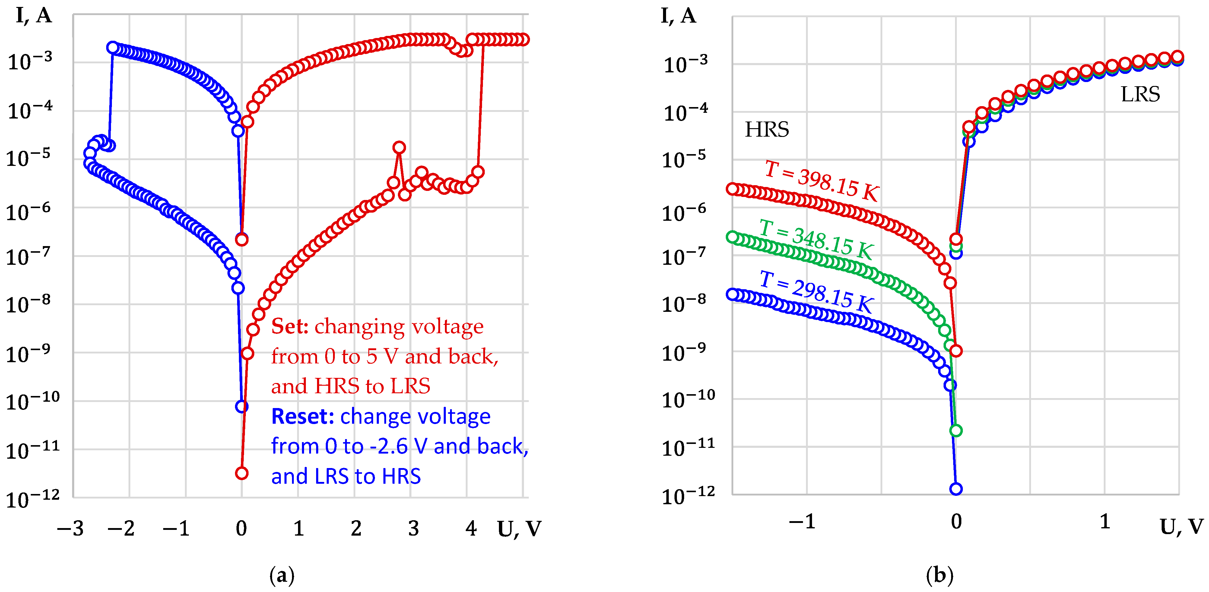
  • Reproducible bipolar switching (Figure 3a);
    Figure 3. VACs of memristors: (a) VAC of one of the switching cycles at room temperature; (b) VACs at three temperatures for HRS and LRS.
  • VACs measurement at temperatures of 298.15 K, 348.15 K, and 398.15 K (Figure 3b);
  • VAC approximation using the SCLC model with uniform distribution of traps [10] described by following Equations (1)–(4);
  • Structure parameters obtained from the approximation, including the effective radius of 100 µm in HRS and 46 nm in LRS.
I U n i = I O h m + I S C L C = S e μ n U d + S 9 8 μ ε ε 0 θ U 2 d 3 ,
n = 2 N d 1 + 1 + 4 g N d N c e x p E a k T ,
N c = 2 2 π m * k T h 2 3 / 2 ,
θ = 1 1 + N t N c e x p W t k T ,
where I O h m is the ohmic current, I S C L C is the SCLC current, S is the area involved in charge transfer, e is the charge of an electron, μ is the electron mobility, U is the applied voltage, d is the dielectric thickness, ε is the static dielectric constant, ε 0 is the vacuum permittivity, n is the free electron concentration inside the dielectric layer, N d is the concentration of donors, g is the degeneracy coefficient, E a is the donor activation energy, k is Boltzmann’s constant, T is temperature, m * is the effective mass of the electron, h is Planck’s constant, θ is the free charge carrier fraction of all injected carriers (free and trapped), N t is the trap concentration, N c is the effective density of states, and W t is the trap energy.
The current is determined by current density multiplied by the effective area in charge transfer S . The effective area of a circular shape is characterized by its effective radius. Reducing the effective radius leads to a resistance increase. The effective radius in the HRS must be smaller than in the LRS. The results in [13] are not consistent with this statement. Therefore, we had to refine the approximation model by considering the exponential and Gaussian distribution of traps for the SCLC model [14,34].
We multiplied the area involved in the charge transfer by the current density from [22] to obtain the current value (5). It is possible to obtain the distribution parameters for the exponential and Gaussian laws after calculating the parameter l using Formulas (6) and (7).
I G a u , E x p = S e 1 l μ N c 2 l + 1 l + 1 l + 1 l ε ε 0 l + 1 N t l U l + 1 d 2 l + 1   ,
l E x p = T c T ,
l G a u = 2 π 16 σ t k T ,
where l —is the parameter that is equal to l E x p in the case of exponential distribution and l G a u in the case of Gaussian distribution, T c —is a temperature parameter that characterizes the exponential trap distribution, the so-called “Characteristic Temperature of Trap Distribution”, and σ t —is the standard deviation of the Gaussian distribution. This Equation (5) at l = 1 looks like I S C L C in (1) for the uniform law, but uses the multiplier N c / N t instead of θ .
In [5], it is determined that in the case of high voltages for HRS and the exponential law of the trap distribution, the current I is presented by the sum of Equations (1) and (5). At that, N c is applied instead of N t in the denominator of Equation (5).
In Section 4.1, we approximated the VAC branches in Figure 3b using expression (5) by adjusting the effective radius and the parameter l , which determines the slope angle of the approximated VAC. Then, using MAPE, we selected the more accurate version of the approximation from those calculated by expression (1) and expression (5).

3.3. Determining the State Retention Time for LRS

There are various methods for estimating the storage time of the resistive states that do not require significant time expenditure. A common and well-proven method [35] uses the Arrhenius Equation (8), which involves testing the sample at elevated temperatures.
t e x p E a k T
Here, the time t is proportional to the exponent of the activation energy E a of the processes in the resistive-switching memory devices, k is the Boltzmann constant, and T is the device temperature.
A common way to assess retention is to heat the structure to a high temperature (up to 730 K, for example), which it can withstand, for example, for a day or more [36]. Resistance is measured for the duration of high-temperature exposure until the point of structural failure. The next sample is then tested at a temperature that was changed by a certain amount. The result is a family of resistance versus time plots, each plot at a particular constant temperature.
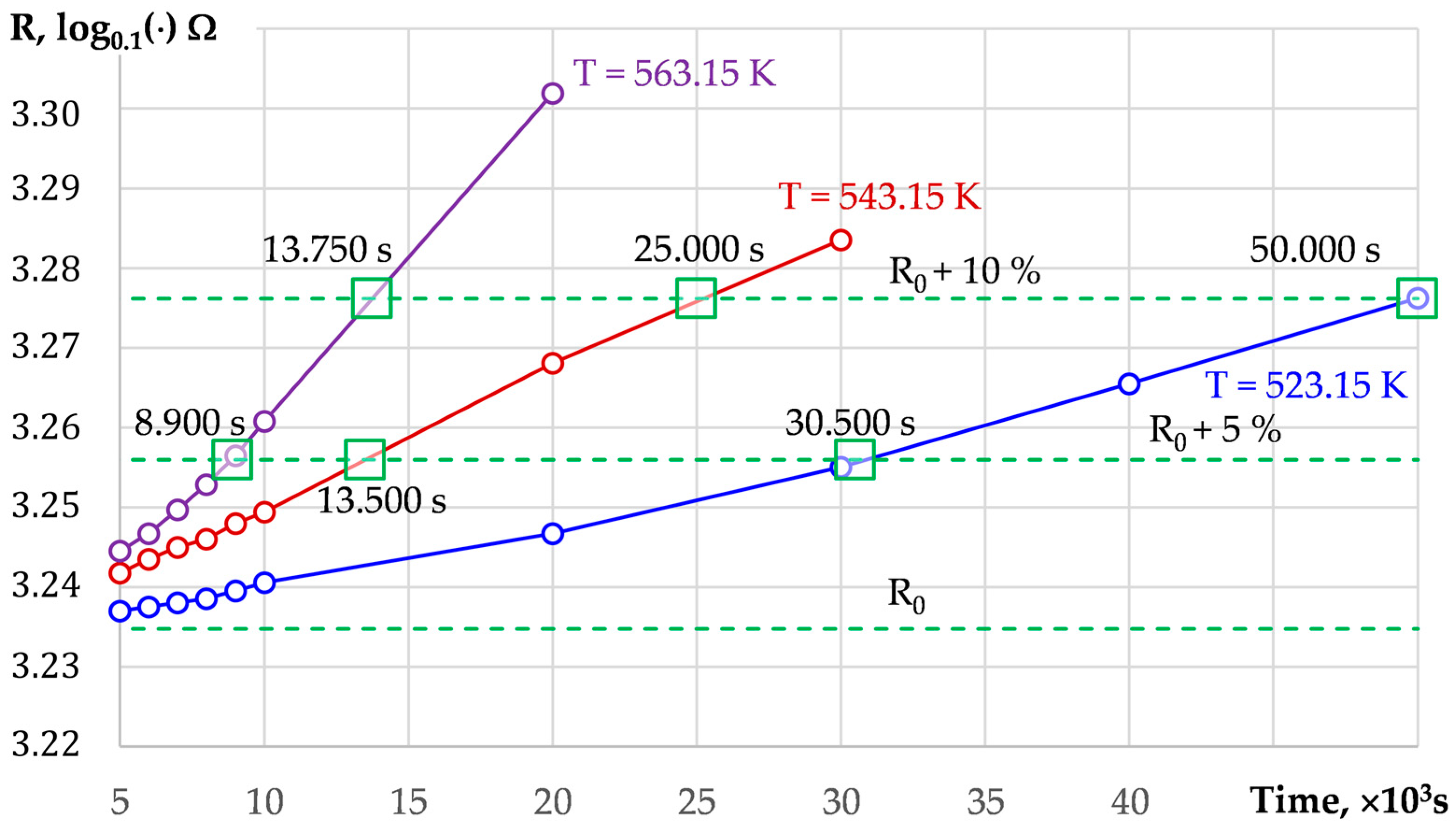
We performed similar measurements at 563.15 K, 543.15 K, and 532.15 K (Figure 4). However, instead of waiting for the sample to fail, we noted time points at which the resistance of the sample increased by 5% and 10% of the readings at the initial moment. In Figure 4, the initial and increased resistance values R 0 are shown by the green dashed lines. The six points of intersection of the resistance vs. time plots with these lines are marked by squares indicating the corresponding time. In Section 4.2, we used the six points in Figure 4 and Arrhenius equation to assess the LRS retention over 10 years.
Figure 4. The time dependence of resistance at LRS and high temperatures.

4. Results and Discussion

4.1. Approximation of the VACs with the SCLC Model in the Case of Exponential and Gaussian Laws of Trap Distributions

Let us consider applying expression (5) to approximate the VAC in the case of a circular section S = π r 2 ,   where r is the effective radius of the conductive zone between the top and bottom electrodes. The rest of the parameters for the calculation are taken from [13]: d = 4 nm; ε = 7 ; m * = 0.5 · m e , where m e is electron mass; μ H R S = 2.5 · 10 4   cm 2 / V · s ; μ L R S = 1 · 10 4   cm 2 / V · s ; E a H R S = 1.456 · 10 19 J; E a L R S = 0.064 · 10 19 J; W t = 0.8 · 10 19 J; g = 2 ; N d H R S = 1 · 10 25   m 3 ; N d L R S = 7 · 10 25   m 3 ; N t = 5 · 10 24   m 3 .
We used the simplex search method [37] to obtain the closest fit of the VAC to the experimental data. In [5], it was stated that the VAC can be approximated by the sum of expressions (1) and (5). We performed such calculations. For HRS the obtained three terms have orders of 10−31, 10−13, and 10−6, respectively. The first two terms are negligible and may be omitted. For the LRS, the approximation function with the three terms does not fit the experimental VAC. In this case, even at l = 0 , the graph does not rotate by an angle sufficient to fit the VAC. Therefore, we used expression (5) without taking into account expression (1) to approximate the VAC.
Using the MAPE algorithm [38], we calculated the errors of our approximation for expression (5) MAPEGau,Exp and the approximation from [13] for expression (1) MAPEUni (Table 1). For all six VACs, the approximation error of MAPEGau,Exp is at least 53 % less than MAPEUni, and therefore our approximation is more accurate.
Table 1. Values of calculated parameters for I G a u , E x p and comparison of approximation accuracy with I U n i .
Note that in HRS the effective radius r at different temperatures is around 1 nm, while in LRS the parameter r is about 60 nm. As noted above, the effective radius for HRS must be smaller than the LRS. From this point of view, our values are adequate. Our value of the effective radius for LRS is in agreement with the value from [13]. The effective radius value of 100 μm obtained in [13] for HRS should be replaced by our value of 1 nm.
Further calculation of the distribution law parameters can be performed using expressions (9) and (10) [39,40] calculated as T c and σ t (Table 1).
D t G a u E = N t 2 π σ t e x p E E c E t 2 2 σ t 2 ,
D t E x p E = N t k T c e x p E c E k T c ,
where D t G a u , D t E x p are the Gaussian and exponential distributions of trap states, E is the considered energy, E c is the energy of the conduction band, and E t is the center of trap distribution.
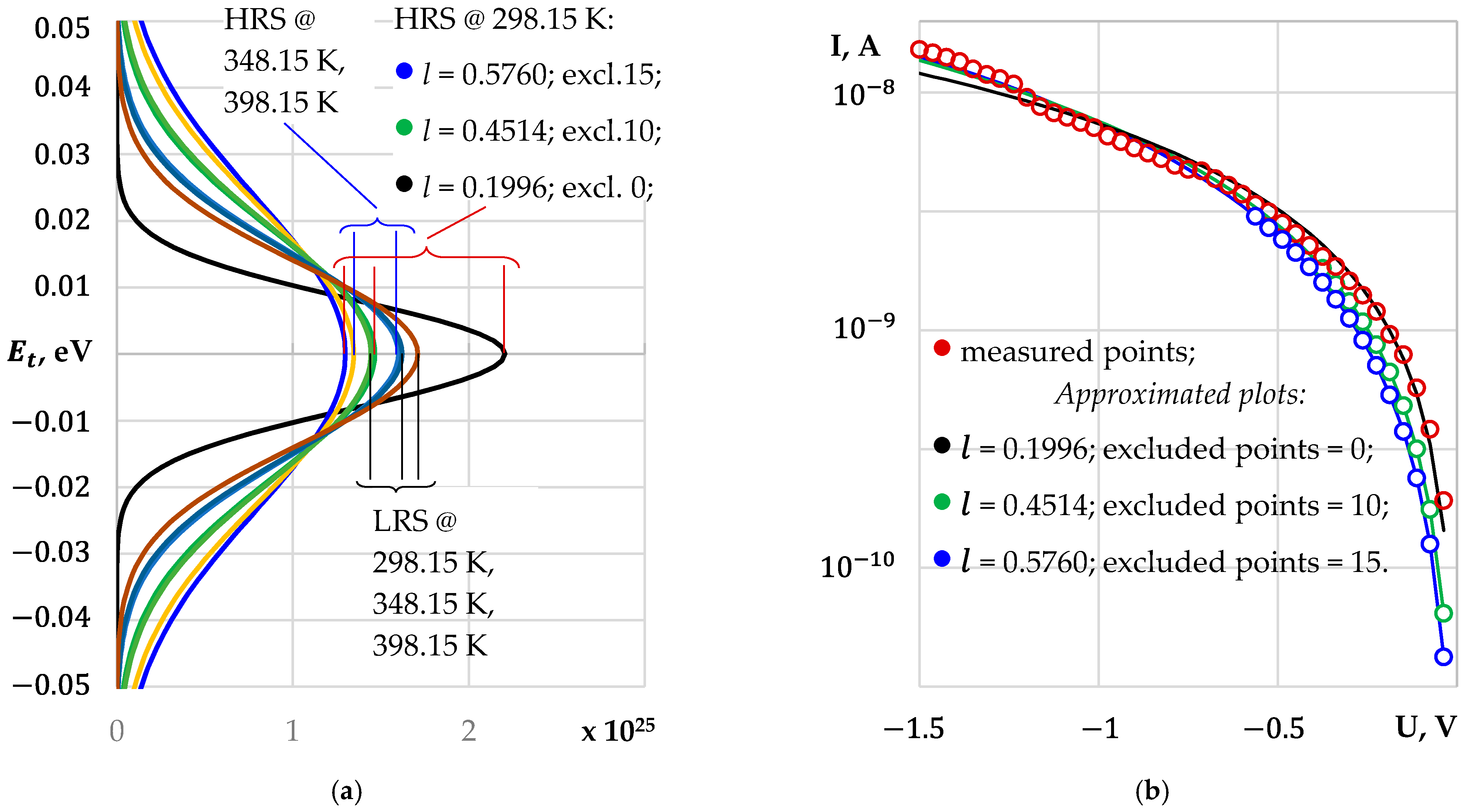
Figure 5 shows the Gaussian distribution of trap states at different temperatures for LRS and HRS according to (9). With increasing temperature, the parameter reflecting the slope of the VAC decreases (Table 1). Thus, according to Ohm’s law, the resistance of our structure decreases with increasing temperature. Consequently, the maximum of the Gaussian distribution of trap states grows (Figure 5a), and trap states tend to occupy energy levels as close to the level as possible.
Figure 5. Gaussian distribution of trap states at different temperatures for LRS and HRS. For LRS, an increase in temperature leads to an increase in the maximum of the probability density function (a). For HRS, this temperature dependence is expected but not present. The black plot maximum for 298.15 K exceeds the yellow plot maximum for 348.15 K. Examining the approximation plot (black) and the experimental plot (red dots), we see the need to rotate the VAC clockwise (b). Excluding the first 10 experimental data points in the low-voltage region gives green plots in (b,a) with l = 0.4514. Excluding the first 15 experimental data points gives l = 0.5760. This results in a reduction in the distribution maximum to the acceptable value (blue plots in (a,b)). The reason for this effect is explained in the text.
Therefore, as the temperature increases, the maximum of the Gaussian distribution of trap states in the HRS state should also increase similarly to the LRS. Figure 5a shows that this dependence holds for temperatures 348.15 K and 398.15 K. The maximum for 298.15 K should have a smaller value than the maximum for 348.15 K, but it is almost two times greater than expected.
To find the cause, we considered the approximation plot (Figure 5b). Red circles represent the experimental data; a solid black curve represents the approximation with l = 0.1996   (Table 1). Increasing the slope of the approximation VAC will reduce the discrepancy with the experimental data. Comparing the red and black curves, we can assume that the slope of the approximated VAR is smaller than the slope of the experimental VAC in the range −1.5…−1.0 V. Obviously, the limiting factor is the experimental data points in the low voltage region.
The exclusion of 15 experimental points gives l = 0.5760   and increases the slope of the VAC for 298.15 K. Thus, the maximum for this temperature (blue curve in Figure 5a) is now smaller than the maximum for 348.15 K. The plot shows the growth of the maxima for HRS with increasing temperature, which is consistent with the similar dependence for LRS.
The need to exclude the low voltage experimental data points at 298.15 K is justified as follows. Of all the six branches of the VAC (Figure 3b), this branch belongs to the region of highest resistance, especially in the low voltage range of 0…−0.5 V. The discrepancy between the experimental values and the approximation could be interpreted by the presence of transient resistance at low voltage levels and low (room) temperature for HRS. The resistance in LRS is significantly lower (difference in effective conductor area radius 0.15 and ~60 nm) than in HRS, so the effect of transient resistance at the same temperature and voltage does not affect the final VAC.
The exclusion of points from the low voltage range of the experimental VAC for HRS at 298.15 K allowed us to obtain refined parameters of the sample: VAC slope parameter l = 0.5760 , effective radius r = 0.11 . These updated values should be used instead of those given above for HRS at 298.15 K in Table 1.
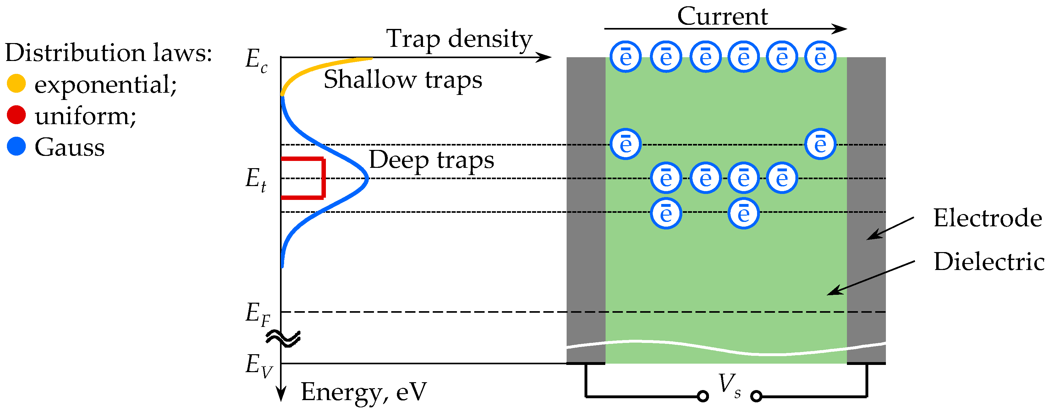
Figure 5a shows the probability density distribution in the case of the exponential law for six cases according to Table 2. It follows from the expression (10) that the maximum of the distribution function is at the energy level of the conduction band E c . This means that in our case the exponential law applies to shallow traps.
Table 2. Parameters for the Gaussian and exponential laws.
However, as mentioned in the Section 2 of this paper, the trap energy in Si3N4 is concentrated in the 1…1.5 eV energy range and is shifted towards the conduction band. Therefore, in our case, the distribution of deep traps is described by a Gaussian law, as shown in Figure 5b.

4.2. Estimation of Temperature Conditions That Allow 10-Year Retention of LRS

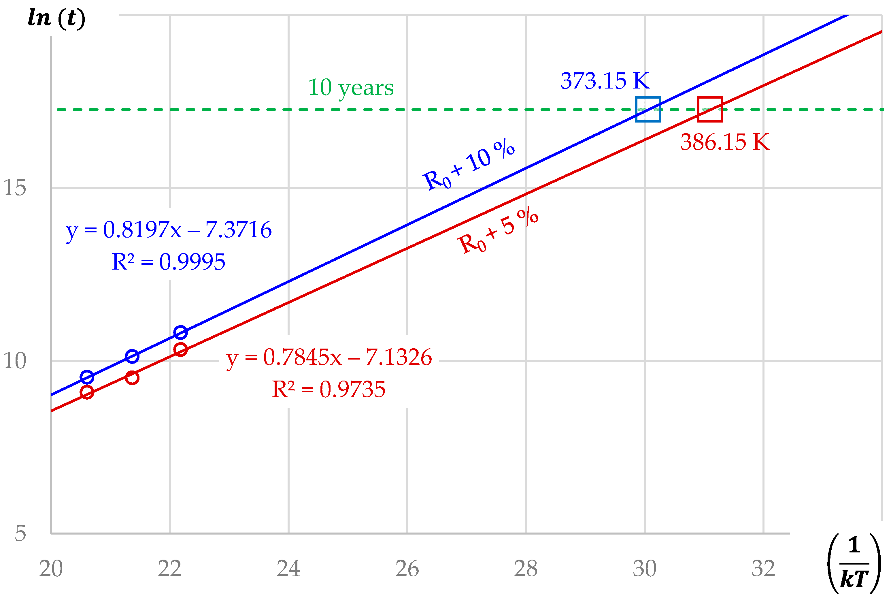
In Section 3.3 we obtained six data points from the resistance vs. time plot, where the resistance of a room temperature memristor increases by 5% or 10% when the sample is heated to 563.15 K, 543.15 K, and 532.15 K. Applying a natural logarithm to the Arrhenius Equation (5), these points are plotted on the ln t vs. 1 / k T plot (Figure 6). Further, we used linear regression to extrapolate two dependencies for R 0 + 5 % and R 0 + 10 % and obtain the values of temperature corresponding to t = 10 years. The linear regression parameters are as follows:
Figure 6. Estimation of temperature conditions that allow 10-year retention of LRS.
  • A slope factor of 0.8197 with an offset of −7.3716 (approximation reliability value R2 = 0.9995) for a 5 % change in resistance;
  • A slope factor of 0.7845 with an offset of −7.1326 (approximation reliability value R2 = 0.9735) for 10% change.
The regressions yield two temperature values, 373.15 K and 386.15 K. These are the temperatures at which it will take 10 years for the resistance to change by 5% and 10%. The 5% and 10% variation in resistance does not affect the ability to distinguish between memristor resistance states. Therefore, we estimated the retention of the memristor to be at least 10 years if it operates at temperatures that do not exceed 386.15 K. These results are consistent with retention parameters of similar Si3N4-based structures [17].

5. Conclusions

Studying our fabricated memristor samples with Ni/Si3N4/SiO2/p+-Si structure, we determined that using the Gaussian distribution of trap states in the SCLC model provides a better experimental data fit and adequate structure parameters. We refined our earlier results and demonstrated up to 53% better MAPE results for VAC current approximation. The approximation results allowed us to establish the effective conductive radius at different temperatures at 1 and 60 nm for HRS and LRS correspondingly. Further, we took additional measurements and studied the change in LRS with time at high temperatures in the 523.15…563.15 K range. We estimate that in 10 years the resistance in LRS would change by 5% at 373.15 K (100 °C) and by 10% at 386.15 K (113 °C).
As mentioned in related work, preserving the resistive state allows applying memristors in crossbars to simulate synaptic weights. The retention value of memristors we studied is comparable to the life cycle of a processor. The endurance is 5000–7000 resistive switching times, which is suitable for applications with a limited number of synaptic weight changes during the life cycle. Such memristors can be used in a simple processor to detect an activation phrase in speech because this phrase is not usually changing. Further work may lie in finding ways of integrating the memristors into the crossbar and interfacing with the CMOS control circuitry.

Author Contributions

Conceptualization, D.M.; methodology, D.M.; software, D.M.; validation, D.Z., F.M. and S.Y.; formal analysis, D.Z.; investigation, D.M.; resources, D.M.; data curation, D.Z.; writing—original draft preparation, D.M.; writing—review and editing, D.Z. and F.M.; visualization, O.T.; supervision, E.G.; project administration, O.T. and E.G.; funding acquisition, O.T. All authors have read and agreed to the published version of the manuscript.

Funding

This research was funded by the Ministry of Science and Higher Education of the Russian Federation, grant number 075-15-2020-791.

Data Availability Statement

Not applicable.

Conflicts of Interest

The authors declare no conflict of interest.

References

  1. Jeong, D.S.; Thomas, R.; Katiyar, R.S.; Scott, J.F.; Kohlstedt, H.; Petraru, A.; Hwang, C.S. Emerging Memories: Resistive Switching Mechanisms and Current Status. Rep. Prog. Phys. 2012, 75, 076502. [Google Scholar] [CrossRef]
  2. Zhuk, M.; Zarubin, S.; Karateev, I.; Matveyev, Y.; Gornev, E.; Krasnikov, G.; Negrov, D.; Zenkevich, A. On-Chip TaOx-Based Non-Volatile Resistive Memory for in Vitro Neurointerfaces. Front. Neurosci. 2020, 14, 94. [Google Scholar] [CrossRef]
  3. Chua, L. Memristor-The Missing Circuit Element. IEEE Trans. Circuit Theory 1971, 18, 507–519. [Google Scholar] [CrossRef]
  4. Strukov, D.B.; Snider, G.S.; Stewart, D.R.; Williams, R.S. The Missing Memristor Found. Nature 2008, 453, 80–83. [Google Scholar] [CrossRef]
  5. Gismatulin, A.A.; Kamaev, G.N.; Kruchinin, V.N.; Gritsenko, V.A.; Orlov, O.M.; Chin, A. Charge Transport Mechanism in the Forming-Free Memristor Based on Silicon Nitride. Sci. Rep. 2021, 11, 2417. [Google Scholar] [CrossRef]
  6. Lee, J.S.; Lee, S.; Noh, T.W. Resistive Switching Phenomena: A Review of Statistical Physics Approaches. Appl. Phys. Rev. 2015, 2, 031303. [Google Scholar] [CrossRef]
  7. Du, N.; Zhao, X.; Chen, Z.; Choubey, B.; Di Ventra, M.; Skorupa, I.; Bürger, D.; Schmidt, H. Synaptic Plasticity in Memristive Artificial Synapses and Their Robustness Against Noisy Inputs. Front. Neurosci. 2021, 15, 660894. [Google Scholar] [CrossRef]
  8. Waser, R.; Dittmann, R.; Menzel, S.; Noll, T. Introduction to New Memory Paradigms: Memristive Phenomena and Neuromorphic Applications. Faraday Discuss. 2019, 213, 11–27. [Google Scholar] [CrossRef]
  9. Gritsenko, V.A. Electronic Structure of Silicon Nitride. Phys. Usp. 2012, 55, 498–507. [Google Scholar] [CrossRef]
  10. Rose, A. Space-Charge-Limited Currents in Solids. Phys. Rev. 1955, 97, 1538–1544. [Google Scholar] [CrossRef]
  11. Vishnyakov, A.V.; Novikov, Y.N.; Gritsenko, V.A.; Nasyrov, K.A. The Charge Transport Mechanism in Silicon Nitride: Multi-Phonon Trap Ionization. Solid-State Electron. 2009, 53, 251–255. [Google Scholar] [CrossRef]
  12. Gritsenko, V.A.; Perevalov, T.V.; Orlov, O.M.; Krasnikov, G.Y. Nature of Traps Responsible for the Memory Effect in Silicon Nitride. Appl. Phys. Lett. 2016, 109, 062904. [Google Scholar] [CrossRef]
  13. Orlov, O.M.; Gismatulin, A.A.; Gritsenko, V.A.; Mizginov, D.S. Charge Transport Mechanism in a Formless Memristor Based on Silicon Nitride. Russ. Microelectron. 2020, 49, 372–377. [Google Scholar] [CrossRef]
  14. Voronkovskii, V.A.; Aliev, V.S.; Gerasimova, A.K.; Islamov, D.R. Conduction Mechanisms of TaN/HfOx/Ni Memristors. Mater. Res. Express 2019, 6, 076411. [Google Scholar] [CrossRef]
  15. Teplov, G.; Zhevnenko, D.; Meshchaninov, F.; Kozhevnikov, V.; Sattarov, P.; Kuznetsov, S.; Magomedrasulov, A.; Telminov, O.; Gornev, E. Memristor Degradation Analysis Using Auxiliary Volt-Ampere Characteristics. Micromachines 2022, 13, 1691. [Google Scholar] [CrossRef]
  16. Sebastian, A.; Le Gallo, M.; Khaddam-Aljameh, R.; Eleftheriou, E. Publisher Correction: Memory Devices and Applications for in-Memory Computing. Nat. Nanotechnol. 2020, 15, 812. [Google Scholar] [CrossRef]
  17. James, A.P. (Ed.) Deep Learning Classifiers with Memristive Networks: Theory and Applications. In Modeling and Optimization in Science and Technologies; Springer International Publishing: Cham, Switzerland, 2020; Volume 14, ISBN 9783030145224. [Google Scholar]
  18. Kim, D.; Kim, S.; Kim, S. Logic-in-Memory Application of CMOS Compatible Silicon Nitride Memristor. Chaos Solitons Fractals 2021, 153, 111540. [Google Scholar] [CrossRef]
  19. Xing, Z.; Zhang, C.; Cui, H.; Hai, Y.; Wu, Q.; Min, D. Space Charge Accumulation and Decay in Dielectric Materials with Dual Discrete Traps. Appl. Sci. 2019, 9, 4253. [Google Scholar] [CrossRef]
  20. Tzeng, S.-D.; Gwo, S. Charge Trapping Properties at Silicon Nitride/Silicon Oxide Interface Studied by Variable-Temperature Electrostatic Force Microscopy. J. Appl. Phys. 2006, 100, 023711. [Google Scholar] [CrossRef]
  21. Haneef, H.F.; Zeidell, A.M.; Jurchescu, O.D. Charge Carrier Traps in Organic Semiconductors: A Review on the Underlying Physics and Impact on Electronic Devices. J. Mater. Chem. C 2020, 8, 759–787. [Google Scholar] [CrossRef]
  22. Steiger, J.; Schmechel, R.; von Seggern, H. Energetic Trap Distributions in Organic Semiconductors. Synth. Met. 2002, 129, 1–7. [Google Scholar] [CrossRef]
  23. Zhang, X.-G.; Pantelides, S.T. Theory of Space Charge Limited Currents. Phys. Rev. Lett. 2012, 108, 266602. [Google Scholar] [CrossRef]
  24. Krasnikov, G.Y. Distinctive features and problems of CMOS technology for decrease in the node size to 0.18 μm or less. Nanotechnol. Russ. 2008, 3, 502–506. [Google Scholar] [CrossRef]
  25. Sun, B.; Ranjan, S.; Zhou, G.; Guo, T.; Xia, Y.; Wei, L.; Zhou, Y.N.; Wu, Y.A. Multistate Resistive Switching Behaviors for Neuromorphic Computing in Memristor. Mater. Today Adv. 2021, 9, 100125. [Google Scholar] [CrossRef]
  26. Kim, S.; Kim, H.; Hwang, S.; Kim, M.-H.; Chang, Y.-F.; Park, B.-G. Analog Synaptic Behavior of a Silicon Nitride Memristor. ACS Appl. Mater. Interfaces 2017, 9, 40420–40427. [Google Scholar] [CrossRef]
  27. Kim, S.; Jung, S.; Kim, M.-H.; Cho, S.; Park, B.-G. Resistive Switching Characteristics of Si3N4 -Based Resistive-Switching Random-Access Memory Cell with Tunnel Barrier for High Density Integration and Low-Power Applications. Appl. Phys. Lett. 2015, 106, 212106. [Google Scholar] [CrossRef]
  28. Chang, Y.-F.; Fowler, B.; Chen, Y.-C.; Zhou, F.; Wu, X.; Chen, Y.-T.; Wang, Y.; Xue, F.; Lee, J.C. Resistive Switching Characteristics and Mechanisms in Silicon Oxide Memory Devices. Phys. Sci. Rev. 2016, 1, 1–9. [Google Scholar] [CrossRef]
  29. Tikhov, S.V.; Mikhaylov, A.N.; Belov, A.I.; Korolev, D.S.; Antonov, I.N.; Karzanov, V.V.; Gorshkov, O.N.; Tetelbaum, D.I.; Karakolis, P.; Dimitrakis, P. Role of Highly Doped Si Substrate in Bipolar Resistive Switching of Silicon Nitride MIS-Capacitors. Microelectron. Eng. 2018, 187–188, 134–138. [Google Scholar] [CrossRef]
  30. Rajbhar, M.K.; Rajamani, S.; Singh, S.K.; Surodin, S.; Nikolichev, D.; Kryukov, R.; Korolev, D.; Nikolskaya, A.; Belov, A.; Nezhdanov, A.; et al. Gallium Nitride Nanocrystal Formation in Si3N4 Matrix by Ion Synthesis. Bull. Mater. Sci. 2020, 43, 234. [Google Scholar] [CrossRef]
  31. Wei, N.; Ding, X.; Gao, S.; Wu, W.; Zhao, Y. HfOx/Ge RRAM with High ON/OFF Ratio and Good Endurance. Electronics 2022, 11, 3820. [Google Scholar] [CrossRef]
  32. Wan, W.; Kubendran, R.; Schaefer, C.; Eryilmaz, S.B.; Zhang, W.; Wu, D.; Deiss, S.; Raina, P.; Qian, H.; Gao, B.; et al. A Compute-in-Memory Chip Based on Resistive Random-Access Memory. Nature 2022, 608, 504–512. [Google Scholar] [CrossRef] [PubMed]
  33. Krishnan, G.; Mandal, S.K.; Pannala, M.; Chakrabarti, C.; Seo, J.-S.; Ogras, U.Y.; Cao, Y. SIAM: Chiplet-Based Scalable In-Memory Acceleration with Mesh for Deep Neural Networks. ACM Trans. Embed. Comput. Syst. 2021, 20, 1–24. [Google Scholar] [CrossRef]
  34. NeŠpůrek, S.; Smejtek, P. Space-Charge Limited Currents in Insulators with the Gaussian Distribution of Traps. Czech J. Phys. 1972, 22, 160–175. [Google Scholar] [CrossRef]
  35. Loy, D.J.J.; Dananjaya, P.A.; Hong, X.L.; Shum, D.P.; Lew, W.S. Conduction Mechanisms on High Retention Annealed MgO-Based Resistive Switching Memory Devices. Sci. Rep. 2018, 8, 14774. [Google Scholar] [CrossRef]
  36. Jiang, H.; Han, L.; Lin, P.; Wang, Z.; Jang, M.H.; Wu, Q.; Barnell, M.; Yang, J.J.; Xin, H.L.; Xia, Q. Sub-10 Nm Ta Channel Responsible for Superior Performance of a HfO2 Memristor. Sci. Rep. 2016, 6, 28525. [Google Scholar] [CrossRef]
  37. Lagarias, J.C.; Reeds, J.A.; Wright, M.H.; Wright, P.E. Convergence Properties of the Nelder—Mead Simplex Method in Low Dimensions. SIAM J. Optim. 1998, 9, 112–147. [Google Scholar] [CrossRef]
  38. de Myttenaere, A.; Golden, B.; Le Grand, B.; Rossi, F. Mean Absolute Percentage Error for Regression Models. Neurocomputing 2016, 192, 38–48. [Google Scholar] [CrossRef]
  39. Nicolai, H.T.; Mandoc, M.M.; Blom, P.W.M. Electron Traps in Semiconducting Polymers: Exponential versus Gaussian Trap Distribution. Phys. Rev. B 2011, 83, 195204. [Google Scholar] [CrossRef]
  40. Kim, T.H.; Park, I.H.; Lee, J.D.; Shin, H.C.; Park, B.-G. Electron Trap Density Distribution of Si-Rich Silicon Nitride Extracted Using the Modified Negative Charge Decay Model of Silicon-Oxide-Nitride-Oxide-Silicon Structure at Elevated Temperatures. Appl. Phys. Lett. 2006, 89, 063508. [Google Scholar] [CrossRef]
Disclaimer/Publisher’s Note: The statements, opinions and data contained in all publications are solely those of the individual author(s) and contributor(s) and not of MDPI and/or the editor(s). MDPI and/or the editor(s) disclaim responsibility for any injury to people or property resulting from any ideas, methods, instructions or products referred to in the content.

Article Metrics

Citations

Article Access Statistics

Multiple requests from the same IP address are counted as one view.