Article

Monolayer TiNI with Anisotropic Optical and Mechanical Properties

1
School of Physics and Technology, University of Jinan, Jinan 250022, China
2
School of Physics, Shandong University, Jinan 250100, China
*
Author to whom correspondence should be addressed.
Crystals 2022, 12(9), 1202; https://doi.org/10.3390/cryst12091202
Submission received: 28 July 2022 / Revised: 19 August 2022 / Accepted: 22 August 2022 / Published: 26 August 2022
(This article belongs to the Special Issue Phase Engineering of Two-Dimensional Lattices)

Abstract

:
Anisotropic monolayer materials have always been investigated by physical researchers. In this paper, we report a stable two-dimensional TiNI monolayer with anisotropic mechanical, optical, and electrical conduction properties. By combining the methods of non-equilibrium Green’s function and density function theory, we obtain two-dimensional TiNI materials with mechanical, optical, and electronic transport properties that depend on the lattice orientation. In addition, the maximum Young’s modulus of the single-layer TiNI can reach 160 N/m2. The calculate result of electrical transport properties also indicates the anisotropic electron transport performance of TiNI monolayer. Moreover, the electron transport intensity along the direction b is about six times the conduction intensity along the direction a. The anisotropic mechanical and optical properties, as well as the tunable band gap and special electron transport characteristics, enable a promising future for monolayer TiNI materials in nano-optoelectronics.

1. Introduction

Two-dimensional materials have attracted a lot of public interest since graphene was first discovered. Many innovative two-dimensional materials have been reported in the fields of energy conservation, bio-physics, and photodetection [1,2,3,4,5,6,7,8,9,10,11]. The laminated material has a number of electronic features that are seldom found in bulk materials. The layered materials are suitable for various optoelectronic devices, like field-effect transistors, because of their desirable electronic performance. The single layer materials with anisotropic electronic properties, especially those with highly anisotropic electrical transport characteristics and carrier mobility, have attracted the attention of researchers [12,13]. Anisotropy in electron transport and optical absorption is a key characteristic of materials. At present, anisotropic materials have been applied in various fields [14,15]. In addition, GaTe with plane anisotropy shows the optical anisotropy in the plane [16,17]. By exerting strain engineering in various directions, it can effectively enhance the performance of phosphonene in various anisotropic mechanical and electronic aspects [18]. Materials that have anisotropic characteristics in terms of mechanics and optoelectronics are highly desirable for real applications. The material offers new possibilities for semiconductor energy conversion. However, one obvious drawback of graphene during its actual implementation in the optoelectronics devices is that even though graphene has a high Fermi speed, it has a bandwidth of zero, which makes its performance in optoelectronic transitions quite inferior [19,20]. In addition, the lack of adjustable bandgap will mean great limitations in practical applications, and the two-dimensional semiconductor with adjustable narrow band gap is more favorable for effective use of light [21].
In recent years, transition metal nitrides (TMNs) with high melting point, high hardness and excellent electrical and thermal conductivity have attracted extensive attention. Because of the small radius of N atoms, they occupy the space between them when forming compounds with transition metals, so the addition of N atoms does not affect the compact arrangement of metal atoms. This makes the extranuclear electron structure of the transition metal more similar to that of the precious metals Pb and Pt with catalytic activity, thus ensuring the same conductivity of TMNs as the metal parent. Meanwhile, the transition metal nitrides have strong chemical bonds between metal atoms and nitrogen atoms, which makes TMNs exhibit strong stability, corrosion resistance, and mechanical strength [22,23,24]. These characteristics give TMNs a strong potential for electrocatalysis applications. In the last few years, two-dimensional C3N with one nitrogen atom and three carbon atoms was prepared and it was found that the material has excellent photoelectronic, mechanical and thermal properties [25,26,27]. In 2018, Meysam Makaremi et al., based on first-principles calculation method, studied the newly prepared two-dimensional carbon and nitrogen compounds, and adjusted the electronic structure and optical absorption capacity through doping and other methods [28]. However, most of the common studies on TMNs are binary compounds, and there are few studies on ternary compounds of TMNs, such as Co4N, Ni3N, Ni3FeN, etc. [29,30,31,32]. The related research of TMNs on the first-principles calculation of ternary transition metal nitrides needs further study.
We have forecasted a novel TiNI, a layered 2D material, based on first-principles computational theory. Phonon spectrum simulation was used to test the dynamic stability of two-dimensional TiNI, and the possibility of its synthesis was evaluated by calculating the binding energy. Then, we have comprehensively investigated the two-dimensional TiNI in the intrinsic state in terms of electronic energy band, mechanomechanical, and optical absorption properties, hoping to obtain anisotropic results in optical, mechanical, and electron transport properties of the material. Simultaneously, the strain engineering applied to the monolayer TiNI enables the modulation of the energy band gap. Our results provide a new monolayer ternary material with rich anisotropy. We hope that our research will provide theoretical guidance in the actual implementation of optoelectronic materials.

2. Methods

The theoretical calculations are performed by using the Vienna Ab initio program package (VASP) on the basis of first principles [33]. The exchange-correlation potential is adopted in the Perdew-Burke-Ernzerhof (PBE) form of the generalized gradient approximation (GGA) and the projection augmented wave (PAW) method [34]. The strong interatomic interaction was corrected by GGA + U. The interaction between ions and electrons is expressed using the projector-enhanced wave method with an energy cutoff of 500 eV [35,36]. The phonon dispersion curve is measured in the program package of PHONOPY code with the supercell technique [37,38]. The convergence criteria for force and energy have been adjusted to 0.001 eV/Å and 10−6 eV, correspondingly. Γ-centered Monkhorst-Pack k-sampling grids of 9 × 9 × 1 is adopted in the Brillouin zone. The positions of the atoms and the lattice constants are sufficiently optimized using the algorithm of conjugate gradients. In the other hand, a vacuum region of 20 Å is inserted in the z-axis direction, in order to prevent interlayer interactions along the z-axis direction. The conduction characteristics are calculated using the nonequilibrium Green’s function, using the atomically localized basis functions and implemented in OpenMX code [39,40]. For different kinds of elements, we use the PAO basis functions of Ti7.0-s2p2d1, N5.0-s2p2d1, and I7.0-s2p2d1, separately, and use the completely relativistic conformal pseudopotential and pseudo-atomic orbitals (PAOs) to expand the wave functions [41]. Our theoretical work can be obtained experimentally by epitaxial growth and other methods.

3. Results and Discussion

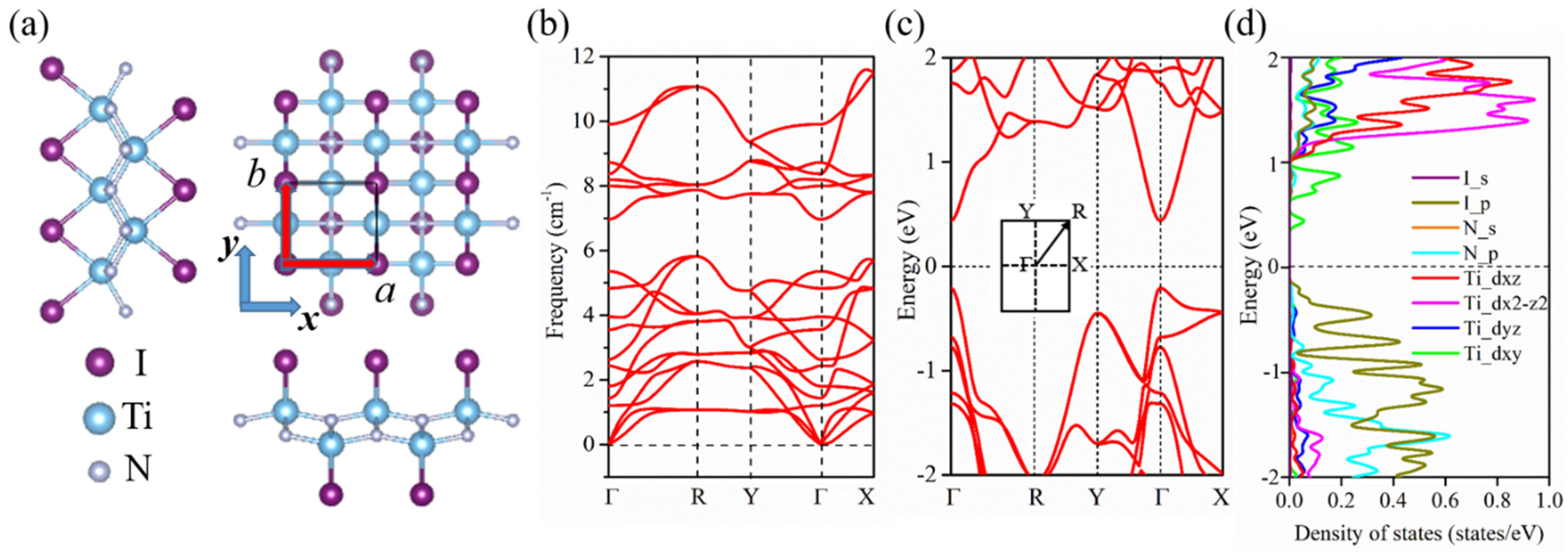
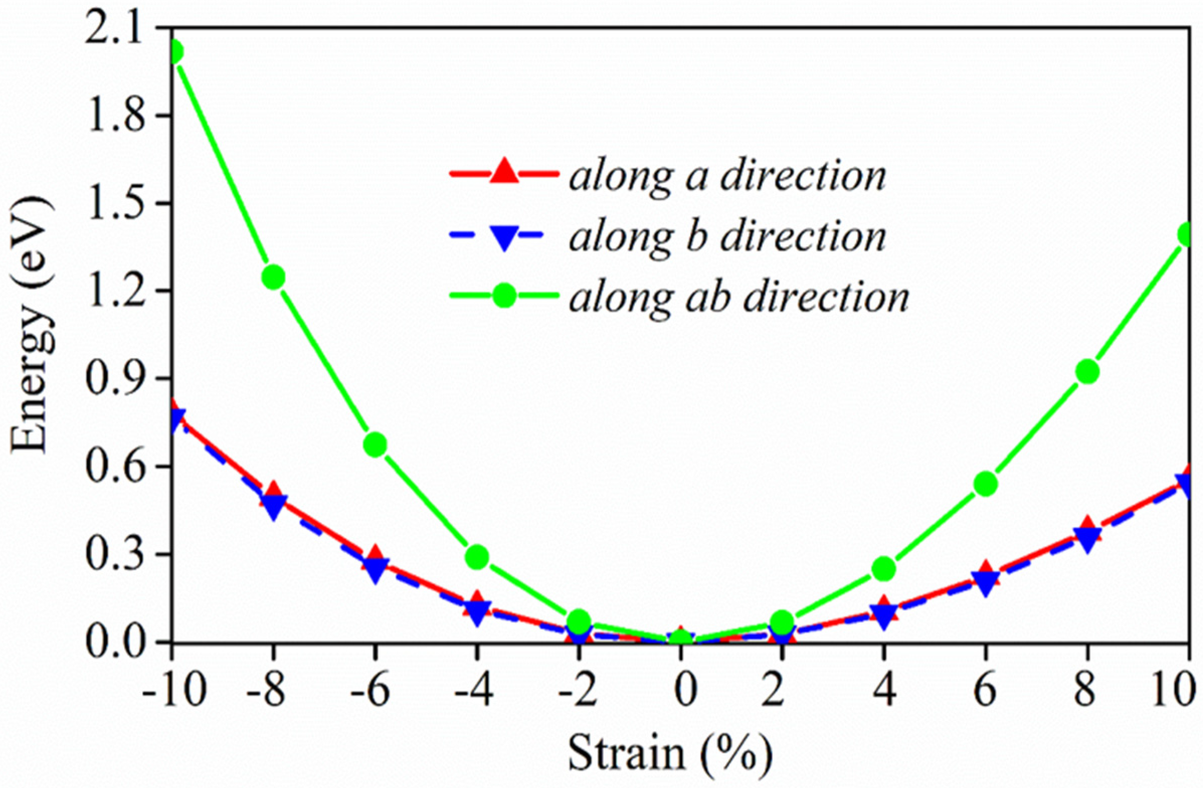
3.1. Energy Band and Structural Stability

We have theoretically predicted a two-dimensional ternary transition metal nitride TiNI. Our fully geometrically optimized monolayer TiNI crystal structure is illustrated in Figure 1a. The colored spheres represent the elements Ti, N, and I. Figure 1a has a black box, which represents a lattice cell, each of which includes two I, N, and Ti atoms. The crystal lattice constants of the material are a = 4.01 Å and b = 3.57 Å, respectively. And ab of TiNI thin film after lattice geometry optimization indicates that monolayer TiNI is structurally anisotropic. The distances between adjacent atoms of the TiNI monolayer are as follows:N–N (2.76 Å), Ti–Ti (3.05 Å), I–I (3.57 Å), Ti–N (2.04 Å), N–I (3.27 Å), and Ti–I (2.84 Å), which are similar to the previous results [42,43]. Firstly, for estimating the robustness of the two-dimensional TiNI material synthesized experimentally, we have computed its cohesive energy, which is calculated as:
E c o h = 2 E T i + 2 E N + 2 E I E T i 2 N 2 I 2 / 6
where ETi, EN, and EI are the individual Ti, N, and I atoms’ energies, respectively. In addition, ETi2N2I2 represents the overall energy of monolayer TiNI. After calculation, the cohesive energy of two-dimensional TiNI is 3.39 eV/Atom. The calculated results are similar to the published cohesion energies of MnNF and black phosphorus [44,45]. The higher the cohesion energy, the easier it is to synthesize in the experiment.
We are capable of seeing in Figure 1b that no imaginary frequencies appear in the phononic spectrum of the laminar TiNI at the highly symmetric Γ points, which indicates the dynamic stability of monolayer TiNI. The kinetic stability further reflects the possibility of TiNI monolayers experimentally. Then, we plotted the electronic energy band structure of the 2D TiNI as illustrated in Figure 1c, where the black illustration indicates our selected condition of the high-symmetry points in the Brillouin zone. According to the diagram of energy band structure, we can see that the layered TiNI has a clear band gap near the Fermi plane, indicating that it is a semiconductor. The conduction band bottom and valence band top located at the same high symmetry point confirms that it is a direct band gap semiconductor with a band gap value of 0.65 eV. Moreover, from the density of states in Figure 1d, we can conclude that the orbital domination states around the Fermi surface are dominantly attributed to the p orbitals of N atoms, the d orbitals of Ti atoms, and the p orbitals of I atoms. Our calculation results are consistent with Wang’s previous calculation conclusions about monolayer TiNI [46], the difference is that we have further explored its anisotropic optical and mechanical properties and electron transport properties.

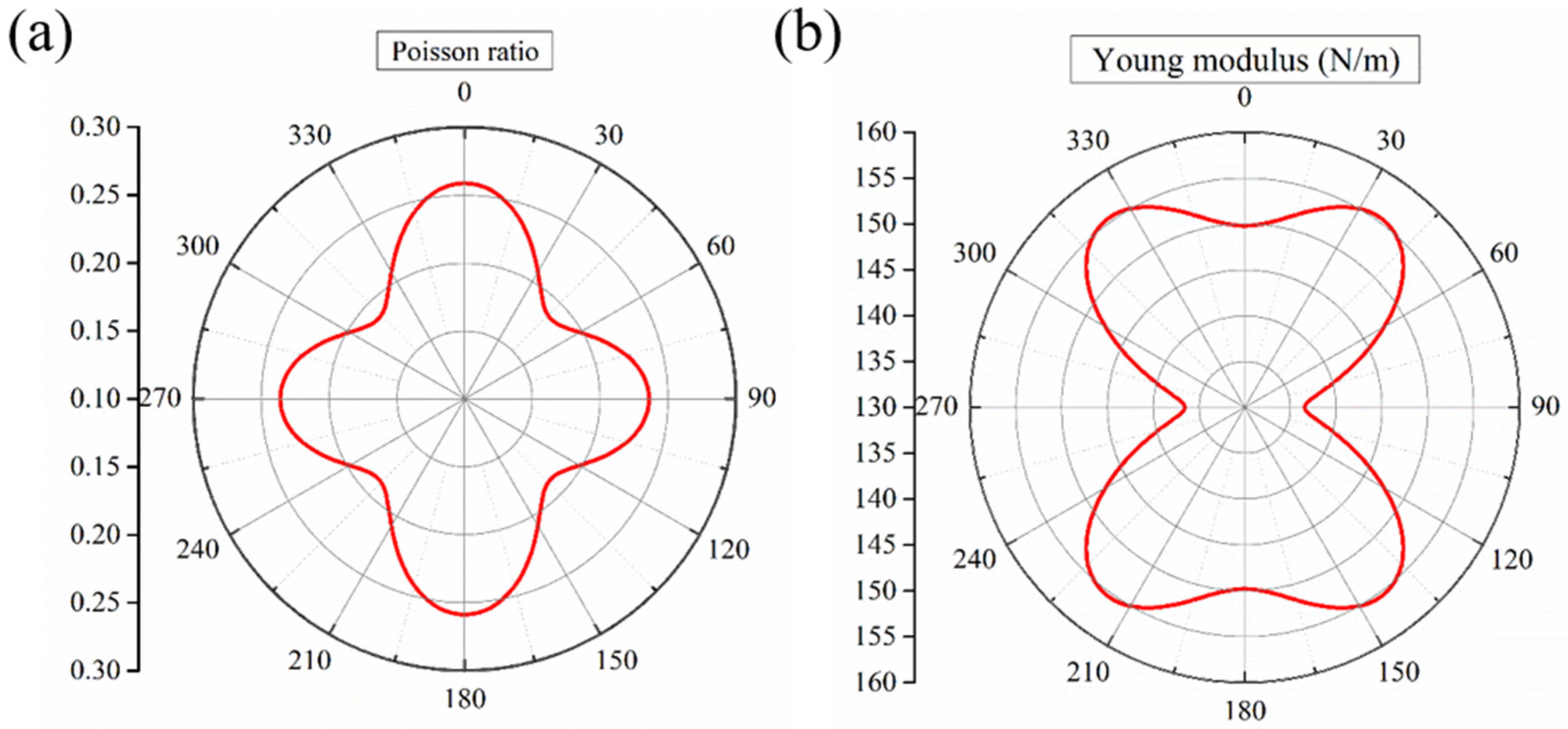
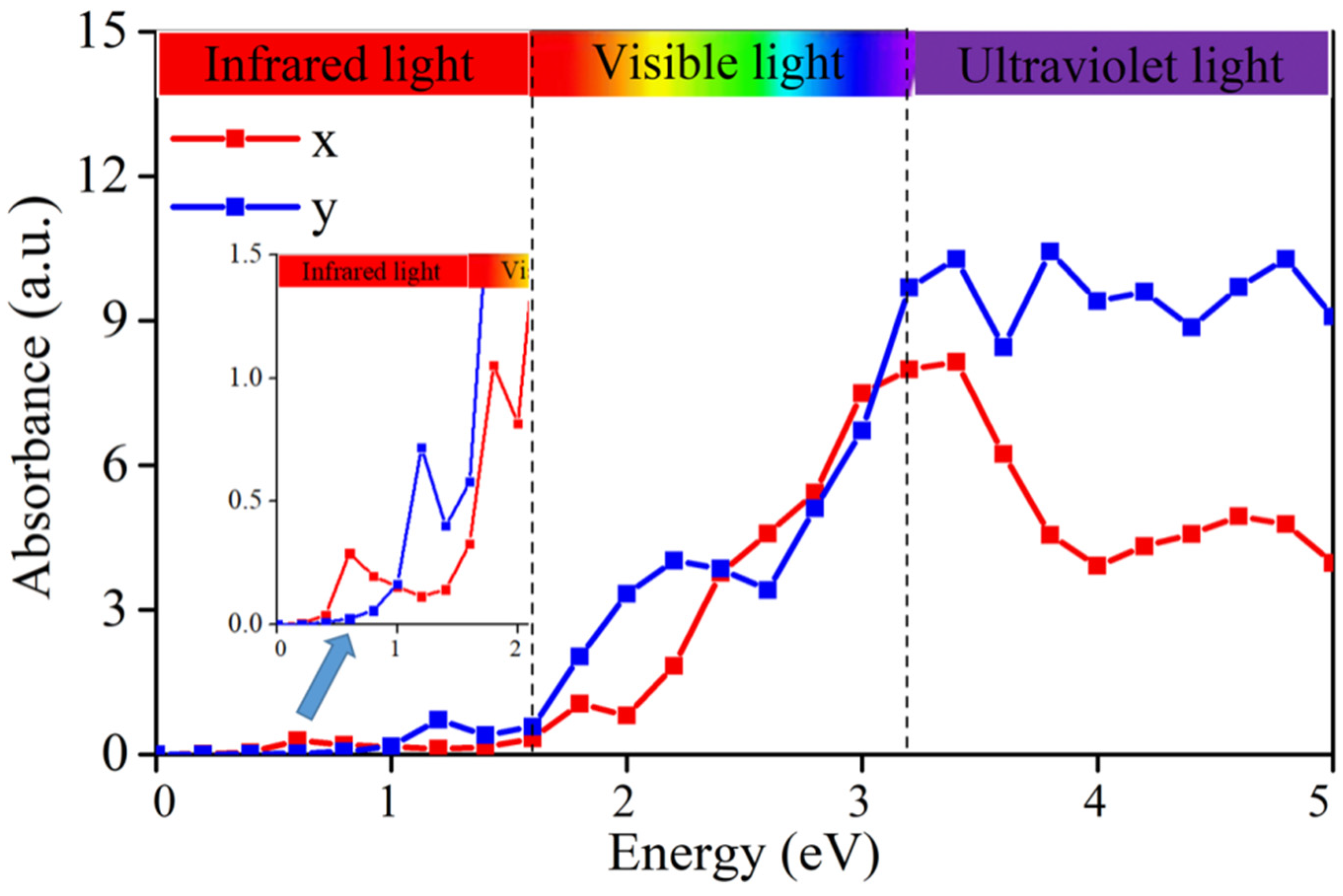
3.2. Mechanical and Optical Properties

Then we continued to investigate the mechanical characteristics of the TiNI films to further evaluate its elastic properties. The four independent elastic constants of two-dimensional TiNI are C11 = 160 N·m−1, C12 = 38 N·m−1, C22 = 145 N·m−1 and C44 = 65 N·m−1 respectively. The elastic constants of laminated TiNI satisfy the Born-Huang criterion (C11C22C122 > 0, C11 > 0, C22 > 0, C44 > 0) [47,48]. This also means that monolayer TiNI meets the equilibrium condition of mechanics, that is, it has mechanical stability. The elastic constants C11 and C22 of laminated TiNI are significantly greater than phosphonene with C11 = 24 N·m−1 and C22 = 103 N·m−1 [49]. On the other hand, the Young’s modulus Y(θ) and Poisson’s ratio υ(θ) along an arbitrary angle θ in the plane satisfy the following equations [47,50]:
Y θ = C 11 C 22 C 12 2 C 11 s i n 4 θ + A s i n 2 θ c o s 2 θ + C 22 c o s 4 θ
υ θ = C 12 s i n 4 θ B s i n 2 θ c o s 2 θ + C 12 c o s 4 θ C 11 s i n 4 θ + A s i n 2 θ c o s 2 θ + C 22 c o s 4 θ
A and B in the equation represent [(C11C22C122)/C44 − 2C12] and [C11 + C22 − (C11C22C122)/C44], respectively. From the Figure 2a,b we can see that the laminated TiNI exhibits various anisotropic Poisson’s ratio υ(θ) and Young’s modulus Y(θ). This indicates that the layered TiNI has a strong mechanical anisotropy. This result is in agreement with the anisotropy of the structure of the material. The higher in-plane Young’s modulus represents the fact that the material possesses many atoms and mutual atomic interactions, which are effective in preventing the curling of the film. After calculation we calculated the Young’s modulus of the monolayer TiNI to be 130~160 N/m2, which is larger than 62 N/m2 of silylene which has been successfully synthesized.
Next, we explore the optical absorption properties of two-dimensional TiNI. The dielectric function reflects the correlation between the energy band and the spectrum of the material, and additionally the analysis of the electron transition between the occupied and unoccupied states helps to research the optical properties of the material. The optical absorption characteristics of the material would be available using the equation ε(ω) = ε1(ω) + 2(ω). Alternatively, the real part of the dielectric function ɛ1(ω) can be acquired by converting the Kramer–Kronig equation. The real or imaginary components of the dielectric function can be accessed by the following equations:
  ε 1 ω = 1 + 2 π P 0 ε 2 ω ω ω 2 ω 2 + i η d ω  
ε 2 ω = 4 π 2 m 2 ω 2 V , C BZ   d 3 k 2 2 π   | e · M CV k | 2   ×   Δ [ E C k E V k ω ]
where ω and m in the equation refer to the angular frequency of the injected photon and the quality of the free electron, respectively. The k represents the reciprocal lattice vector. The energy of the injected photon is denoted by ℏω. BZ refers to the first Brillouin zone. |MCV(k)|2 is the element of the dynamics matrix, where C and V are abbreviations for conduction band and valence band, respectively. EC(k) and EV(k) are the energy at the CB and the VB, respectively. The equation for the coefficient of optical absorption is given by:
α ω = 2 ω + ε 1 2 ω ε 2 2 ω ε 1 ω
where α is the absorption coefficient of the incident light and ω is the angular frequency of the incoming light. As can be seen from the optical absorption spectrum of two-dimensional TiNI in Figure 3, the absorption coefficient increases progressively along with the growth of energy of photons. The first and second peaks of absorption appear at the region of visible light and the region of ultraviolet light, respectively. Optical absorption spectroscopy research has demonstrated the ability of monolayer TiNI to detect ultraviolet and visible light. Moreover, the optical absorption curves of two-dimensional TiNI in x and y directions do not coincide, that is, there are obvious differences. This indicates that the optical absorption capacity of monolayer TiNI is different in x direction and y direction. The anisotropy of optical absorption is also consistent with other anisotropy of the material. Most of the valence band electrons and conduction band electrons of semiconductors are distributed near the forbidden band, so when the photon energy approaches the forbidden band width, a large number of electrons can leap by absorbing photon energy, when the absorption coefficient is positively correlated with the increase in the number of photons. For semiconductor materials, we use absorption spectra to obtain the material optical band gap, following the Tauc Plot method [51]. The calculated optical band gap of material is 0.45 eV. Anisotropic optical absorption characteristics make two-dimensional TiNI have potential application value in the field of photoelectric detection.
Applying strain to a monolayer material can effectively regulate its electronic properties [52,53,54]. In an effort to further investigate the electronic characteristics of monolayer TiNI materials in real-world applications under external strain, the strain is imposed on the two-dimensional TiNI crystal structure. In order to explore whether its electronic band structure performance changes with the strain. The lattice constant of the monolayer TiNI material can be modified by imposing a homogeneous strain, and we define ε = (aa0)/a0, in which a and a0 denote the lattice constants at the strain and equilibrium states, respectively. A variation of energy relations when imposing uniaxial or biaxial strain is shown in Figure 4. It can be seen that two-dimensional TiNI has the lowest energy in the eigenstate (at 0). In combination with the cohesion energy and phonon spectrum calculation discussed before, it can be seen that the eigenstate of the monolayer TiNI after the geometry optimization is the fundamental phase. From the Figure 1, Figure 2 and Figure 3, we can see that the band gap of the monolayer TiNI turns from direct into indirect when a compressive strain of −4% is applied in the a-direction. A band gap change from direct to indirect can also be achieved when stretching strain of 4% is applied in the b-direction along the 2D TiNI. Direct band gap can be transformed into indirect band gap by applying 8% biaxial tensile strain. The result shows that the energy band gap of single-layer TiNI is adjustable through imposing outer strain. This is attributed to the variation of Ti-I bond and Ti-N bond when the crystal structure is compressed or stretched. In addition, the hybridization of atomic orbitals is affected after strain is applied, resulting in the change of band gap of electronic band structure.

3.3. Electronic Transport Properties

The above study found that two-dimensional TiNI exhibits anisotropy in structural, mechanical and optical absorption, and we predict that it may have anisotropy in electron transport. Theoretical calculations are performed by combining the first-principle and the non-equilibrium Green’s function. The current corresponding to the monolayer TiNI at different voltages is calculated using OpenMX software. The electrical conductivity of the system is quantitatively described by drawing the curve of current and voltage (I-V), and the anisotropy of electron transport is further discussed. Firstly, in order to guarantee the accuracy of subsequent calculation using OpenMX software, VASP and OpenMX software were used to calculate the same band of the structure, as shown in Figure 5a. For example, in the schematic diagram of the conduction device model along the a-direction, the electrodes at both ends are 2 × 1 × 1 super cells, the middle scattering area is 10 × 1 × 1 super cells, and the device is 14 × 1 × 1 super cells long in total. Similarly, the electrodes at both ends are 1 × 2 × 1 super cells along the b-direction, the middle scattering area is 1 × 10 × 1 super cells, and the device is 1 × 14 × 1 super cells long in total.
The electron transport model of the two-dimensional material is shown in Figure 5b. We can see that in the model diagram, the two ends of the device are the source and drain, and the middle of the device is the scattering region. In the calculation, we consider the conduction conditions towards the a-direction and the b-direction, respectively. The gate voltage is applied to the middle scattering region according to the designed electron transport model. Moreover, to demonstrate the benefits of the use of single-layer TiNI when it is in a lower voltage state, we set the bias voltage to 0.1~2.0 V, and the currents along a-direction and b-direction were calculated respectively. Through calculation, it is found that the current of single-layer TiNI can reach µA in parallel state, as shown in Figure 5c. The monolayer TiNI has the same level of current values as the recently published 2D IV-V and MnNF that have advanced anisotropic electron transport properties [44,55]. Through the voltammetric characteristic curve in Figure 5c, we can observe the change of conductivity, i.e., by observing the change of slope in the graph, the larger the slope represents the larger the conductivity, the better the conductivity of the material. The anisotropic crystal structure in monolayer TiNI results in the internal inter-atomic bonding anisotropy, which in turn contributes to the distribution of electron anisotropy and ultimately leads to the anisotropy in electron transport properties of two-dimensional TiNI. In addition, the current value can reach 6 µA at a voltage value of 2.0 V.
It can be seen that the conveyance in the orientation towards b is significantly larger than that in the orientation towards a. Transportation current of single-layer TiNI in the direction b is up to six times that in the direction a. In addition, we observe the anisotropy of the voltammetric characteristic curves of materials in the a and b directions by calculating the anisotropy. In addition, we can also analyze the anisotropy transport characteristics through a comparison of charge densities along the a-direction and the b-direction. We can see the charge density distributed in the monolayer TiNI around the Fermi level in Figure 5c. It can be concluded that the extended state is along the direction of b, then the two-dimensional TiNI system is more conductive along the direction of b. This result further proves the anisotropy of monolayer TiNI materials.

4. Conclusions

In conclusion, we have investigated the novel 2D TiNI material by combining the density functional theory and the method of nonequilibrium Green’s function. By calculating the binding energy and phonon spectrum, the possibility of synthesis and dynamic stability of the structure were confirmed. By studying the mechanical properties of two-dimensional TiNI, it is found that two-dimensional TiNI material has anisotropic mechanical properties and good mechanical stability. The maximum Young’s modulus of the monolayer TiNI can reach 160 N/m2. The band gap can be regulated by applying −10~10% strain. At the same time, the current can reach 6 μA when the voltage is 2.0 V. Single-layer TiNI transmits six times more current along the b-direction than along the a-direction. Our theoretical study shows that two-dimensional TiNI has promising applications in anisotropic electronic and optical fields.

Author Contributions

Conceptualization, S.-J.L., M.L., C.-G.Z. and P.-J.W.; Data curation, M.L.; Formal analysis, S.-J.L. and C.-G.Z.; Funding acquisition, P.-J.W.; Investigation, M.L., C.-G.Z. and K.-Y.S.; Methodology, S.-J.L.; Project administration, P.-J.W.; Resources, K.-Y.S.; Software, K.-Y.S.; Supervision, P.-J.W.; Writing—original draft, S.-J.L. and C.-G.Z.; Writing—review & editing, S.-J.L., M.L., K.-Y.S. and P.-J.W. All authors have read and agreed to the published version of the manuscript.

Funding

This research was funded by the National Natural Science Foundation of China (Grant No. 62071200, 11804116) and Science and Technology Foundation of University of Jinan (Grant No. XKY1619) and the Natural Science Foundation of Shandong Province (Grant No. ZR2019MA041) and Taishan Scholar Project of Shandong Province (No. ts20190939).

Institutional Review Board Statement

Not applicable.

Informed Consent Statement

Not applicable.

Data Availability Statement

Not applicable.

Conflicts of Interest

There is no conflict of interest in this manuscript.

References

  1. Radisavljevic, B.; Radenovic, A.; Brivio, J.; Giacometti, V.; Kis, A. Single-layer MoS2 transistors. Nat. Nanotechnol. 2011, 6, 147–150. [Google Scholar] [CrossRef] [PubMed]
  2. Wang, Q.H.; Kalantar-Zadeh, K.; Kis, A.; Coleman, J.N.; Strano, M.S. Electronics and optoelectronics of two-dimensional transition metal dichalcogenides. Nat. Nanotechnol. 2012, 7, 699–712. [Google Scholar] [CrossRef] [PubMed]
  3. Zhang, X.; Zhao, X.; Wu, D.; Jing, Y.; Zhou, Z. High and anisotropic carrier mobility in experimentally possible Ti2CO2 (MXene) monolayers and nanoribbons. Nanoscale 2015, 7, 16020–16025. [Google Scholar] [CrossRef] [PubMed]
  4. Wang, Z.; Hao, Z.; Yu, S.; Huang, C.; Pan, Y.; Zhao, X. A wearable and deformable graphene-based affinity nanosensor for monitoring of cytokines in biofluids. Nanomaterials 2020, 10, 1503. [Google Scholar] [CrossRef]
  5. Wang, Z.; Hao, Z.; Yu, S.; De Moraes, C.G.; Suh, L.H.; Zhao, X.; Lin, Q. An ultraflexible and stretchable aptameric graphene nanosensor for biomarker detection and monitoring. Adv. Funct. Mater. 2019, 29, 1905202. [Google Scholar] [CrossRef]
  6. Dhanabalan, S.C.; Ponraj, J.S.; Zhang, H.; Bao, Q. Present perspectives of broadband photodetectors based on nanobelts, nanoribbons, nanosheets and the emerging 2D materials. Nanoscale 2016, 8, 6410–6434. [Google Scholar] [CrossRef]
  7. Zhang, S.; Zhou, W.; Ma, Y.; Ji, J.; Cai, B.; Yang, S.A.; Zhu, Z.; Chen, Z.; Zeng, H. Antimonene oxides: Emerging tunable direct bandgap semiconductor and novel topological insulator. Nano Lett. 2017, 17, 3434–3440. [Google Scholar] [CrossRef]
  8. Zhang, C.-G.; Ji, W.-X.; Li, P.; Zhang, C.-W.; Wang, P.-J. Tuning the Electronic and Optical Properties of Two-dimensional AgBiP2Se6 and AgInP2Se6 Janus Monolayers. Chem. Phys. Lett. 2021, 780, 138933. [Google Scholar] [CrossRef]
  9. Zhang, C.; Ji, W.; Li, S.; Li, P.; Zhang, C.; Wang, P.-J. 2D ternary nitrides XNY (X = Ti, Zr, Hf; YF, Cl, Br) with applications as photoelectric and photocatalytic materials featuring mechanical and optical anisotropy: A DFT study. J. Solid State Chem. 2021, 303, 122517. [Google Scholar] [CrossRef]
  10. Wang, Z.; Hao, Z.; Wang, X.; Huang, C.; Lin, Q.; Zhao, X.; Pan, Y. A Flexible and regenerative aptameric graphene–Nafion biosensor for cytokine storm biomarker monitoring in undiluted biofluids toward wearable applications. Adv. Funct. Mater. 2021, 31, 2005958. [Google Scholar] [CrossRef]
  11. Wang, Z.; Hao, Z.; Yang, C.; Wang, H.; Huang, C.; Zhao, X.; Pan, Y. Ultra-sensitive and rapid screening of acute myocardial infarction using 3D-affinity graphene biosensor. Cell Rep. Phys. Sci. 2022, 3, 100855. [Google Scholar] [CrossRef]
  12. Guo, S.; Zhang, Y.; Ge, Y.; Zhang, S.; Zeng, H.; Zhang, H. 2D V-V binary materials: Status and challenges. Adv. Mater. 2019, 31, 1902352. [Google Scholar] [CrossRef] [PubMed]
  13. Qu, H.; Guo, S.; Zhou, W.; Zhang, S. Uncovering the anisotropic electronic structure of 2D group VA-VA monolayers for quantum transport. IEEE Electron Device Lett. 2020, 42, 66–69. [Google Scholar] [CrossRef]
  14. Quio, J.; Kong, X.; Hu, Z.; Yang, F.; Ji, W. High-mobility transport anisotropy and linear dichroism in few-layer black phosphorus. Nat. Commun. 2014, 7, 4475. [Google Scholar] [CrossRef] [PubMed]
  15. Quhe, R.; Li, Q.; Zhang, Q.; Wang, Y.; Zhang, H.; Li, J.; Zhang, X.; Chen, D.; Liu, K.; Ye, Y. Simulations of quantum transport in sub-5-nm monolayer phosphorene transistors. Phys. Rev. Appl. 2018, 10, 024022. [Google Scholar] [CrossRef]
  16. Huang, S.; Tatsumi, Y.; Ling, X.; Guo, H.; Wang, Z.; Watson, G.; Puretzky, A.A.; Geohegan, D.B.; Kong, J.; Li, J. In-plane optical anisotropy of layered gallium telluride. ACS Nano 2016, 10, 8964–8972. [Google Scholar] [CrossRef] [PubMed]
  17. Sun, J.; Leng, J.; Zhang, G. The grain boundary effect on mechanical and electronic transport properties of a striped borophene. Phys. Chem. Chem. Phys. 2020, 22, 21844–21850. [Google Scholar] [CrossRef] [PubMed]
  18. Wang, L.; Kutana, A.; Zou, X.; Yakobson, B.I. Electro-mechanical anisotropy of phosphorene. Nanoscale 2015, 7, 9746–9751. [Google Scholar] [CrossRef] [PubMed]
  19. Pan, Y.; Zhang, L.; Huang, L.; Li, L.; Meng, L.; Gao, M.; Huan, Q.; Lin, X.; Wang, Y.; Du, S. Construction of 2D atomic crystals on transition metal surfaces: Graphene, silicene, and hafnene. Small 2014, 10, 2215–2225. [Google Scholar] [CrossRef]
  20. Allen, M.J.; Tung, V.C.; Kaner, R.B. Honeycomb carbon: A review of graphene. Chem. Rev. 2010, 110, 132–145. [Google Scholar] [CrossRef]
  21. Liao, L.; Lin, Y.-C.; Bao, M.; Cheng, R.; Bai, J.; Liu, Y.; Qu, Y.; Wang, K.L.; Huang, Y.; Duan, X. High-speed graphene transistors with a self-aligned nanowire gate. Nature 2010, 467, 305–308. [Google Scholar] [CrossRef] [PubMed]
  22. Zhong, Y.; Xia, X.; Shi, F.; Zhan, J.; Tu, J.; Fan, H.J. Transition metal carbides and nitrides in energy storage and conversion. Adv. Sci. 2016, 3, 1500286. [Google Scholar] [CrossRef] [PubMed]
  23. Ham, D.J.; Lee, J.S. Transition metal carbides and nitrides as electrode materials for low temperature fuel cells. Energies 2009, 2, 873–899. [Google Scholar] [CrossRef]
  24. Cao, B.; Veith, G.M.; Neuefeind, J.C.; Adzic, R.R.; Khalifah, P.G. Mixed close-packed cobalt molybdenum nitrides as non-noble metal electrocatalysts for the hydrogen evolution reaction. J. Am. Chem. Soc. 2013, 135, 19186–19192. [Google Scholar] [CrossRef]
  25. Yang, S.; Li, W.; Ye, C.; Wang, G.; Tian, H.; Zhu, C.; He, P.; Ding, G.; Xie, X.; Liu, Y. C3N-A 2D crystalline, hole-free, tunable-narrow-bandgap semiconductor with ferromagnetic properties. Adv. Mater. 2017, 29, 1605625. [Google Scholar] [CrossRef] [PubMed]
  26. Mortazavi, B. Ultra high stiffness and thermal conductivity of graphene like C3N. Carbon 2017, 118, 25–34. [Google Scholar] [CrossRef]
  27. Makaremi, M.; Mortazavi, B.; Singh, C.V. Adsorption of metallic, metalloidic, and nonmetallic adatoms on two-dimensional C3N. J. Phys. Chem. C 2017, 121, 18575–18583. [Google Scholar] [CrossRef]
  28. Makaremi, M.; Grixti, S.; Butler, K.T.; Ozin, G.A.; Singh, C.V. Band engineering of carbon nitride monolayers by N-type, P-type, and isoelectronic doping for photocatalytic applications. ACS Appl. Mater. Interfaces 2018, 10, 11143–11151. [Google Scholar] [CrossRef]
  29. Gu, Y.; Chen, S.; Ren, J.; Jia, Y.A.; Chen, C.; Komarneni, S.; Yang, D.; Yao, X. Electronic structure tuning in Ni3FeN/r-GO aerogel toward bifunctional electrocatalyst for overall water splitting. ACS Nano 2018, 12, 245–253. [Google Scholar] [CrossRef]
  30. Hu, Y.; Yang, H.; Chen, J.; Xiong, T.; Balogun, M.-S.J.T.; Tong, Y. Efficient hydrogen evolution activity and overall water splitting of metallic Co4N nanowires through tunable d-orbitals with ultrafast incorporation of FeOOH. ACS Appl. Mater. Interfaces 2019, 11, 5152–5158. [Google Scholar] [CrossRef]
  31. Yan, H.; Xie, Y.; Wu, A.; Cai, Z.; Wang, L.; Tian, C.; Zhang, X.; Fu, H. Anion-modulated HER and OER activities of 3D Ni–V-based interstitial compound heterojunctions for high-efficiency and stable overall water splitting. Adv. Mater. 2019, 31, 1901174. [Google Scholar] [CrossRef] [PubMed]
  32. Guan, J.; Li, C.; Zhao, J.; Yang, Y.; Zhou, W.; Wang, Y.; Li, G.-R. FeOOH-enhanced bifunctionality in Ni3N nanotube arrays for water splitting. Appl. Catal. B Environ. 2020, 269, 118600. [Google Scholar] [CrossRef]
  33. Kresse, G.; Furthmüller, J. Efficient iterative schemes for ab initio total-energy calculations using a plane-wave basis set. Phys. Rev. B 1996, 54, 11169. [Google Scholar] [CrossRef] [PubMed]
  34. Perdew, J.P.; Burke, K.; Ernzerhof, M. Generalized gradient approximation made simple. Phys. Rev. Lett. 1996, 77, 3865. [Google Scholar] [CrossRef] [PubMed]
  35. Blöchl, P.E. Projector augmented-wave method. Phys. Rev. B 1994, 50, 17953. [Google Scholar] [CrossRef]
  36. Kresse, G.; Joubert, D. From ultrasoft pseudopotentials to the projector augmented-wave method. Phys. Rev. B 1999, 59, 1758. [Google Scholar] [CrossRef]
  37. Parlinski, K.; Li, Z.; Kawazoe, Y. First-principles determination of the soft mode in cubic ZrO2. Phys. Rev. Lett. 1997, 78, 4063. [Google Scholar] [CrossRef]
  38. Togo, A.; Tanaka, I. First principles phonon calculations in materials science. Scr. Mater. 2015, 108, 1–5. [Google Scholar] [CrossRef]
  39. Ozaki, T.; Nishio, K.; Kino, H. Efficient implementation of the nonequilibrium Green function method for electronic transport calculations. Phys. Rev. B 2010, 81, 035116. [Google Scholar] [CrossRef]
  40. Ozaki, T. Continued fraction representation of the Fermi-Dirac function for large-scale electronic structure calculations. Phys. Rev. B 2007, 75, 035123. [Google Scholar] [CrossRef] [Green Version]
  41. Ozaki, T.; Kino, H. Numerical atomic basis orbitals from H to Kr. Phys. Rev. B 2004, 69, 195113. [Google Scholar] [CrossRef]
  42. Schurz, C.M.; Shlyk, L.; Schleid, T.; Niewa, R. Superconducting nitride halidesMNX(M=Ti, Zr, Hf;X=Cl, Br, I). Kristallogr. Z. 2011, 226, 395–416. [Google Scholar] [CrossRef]
  43. Juzatr, R.; Friedrichsen, H. Die Kristallstruktur von β-ZrNCl and β-ZrNBr. Z. Anorg. Allg. Chem. 1964, 332, 173–178. [Google Scholar] [CrossRef]
  44. Hu, Y.; Li, S.-S.; Ji, W.-X.; Zhang, C.-W.; Ding, M.; Wang, P.-J.; Yan, S.-S. Glide Mirror Plane Protected Nodal-Loop in an Anisotropic Half-Metallic MnNF Monolayer. J. Phys. Chem. Lett. 2019, 11, 485–491. [Google Scholar] [CrossRef] [PubMed]
  45. Chen, P.-J.; Jeng, H.-T. High applicability of two-dimensional phosphorous in Kagome lattice predicted from first-principles calculations. Sci. Rep. 2016, 6, 23151. [Google Scholar] [CrossRef]
  46. Wang, A.; Wang, Z.; Du, A.; Zhao, M. Band inversion and topological aspects in a TiNI monolayer. Phys. Chem. Chem. Phys. 2016, 18, 22154–22159. [Google Scholar] [CrossRef]
  47. Born, M.; Huang, K. Dynamical Theory of Crystal Lattices; Clarendon Press: Oxford, UK, 1954. [Google Scholar]
  48. Wang, J.; Yip, S.; Phillpot, S.; Wolf, D. Crystal instabilities at finite strain. Phys. Rev. Lett. 1993, 71, 4182. [Google Scholar] [CrossRef]
  49. Zhuo, Z.; Wu, X.; Yang, J. Two-dimensional phosphorus porous polymorphs with tunable band gaps. J. Am. Chem. Soc. 2016, 138, 7091–7098. [Google Scholar] [CrossRef]
  50. Cadelano, E.; Palla, P.L.; Giordano, S.; Colombo, L. Elastic properties of hydrogenated graphene. Phys. Rev. B 2010, 82, 235414. [Google Scholar] [CrossRef]
  51. Tauc, J. Optical properties and electronic structure of amorphous Ge and Si. Mater. Res. Bull. 1968, 3, 37–46. [Google Scholar] [CrossRef]
  52. Kaasbjerg, K.; Thygesen, K.S.; Jacobsen, K.W. Phonon-limited mobility in n-type single-layer MoS2 from first principles. Phys. Rev. B 2012, 85, 115317. [Google Scholar] [CrossRef]
  53. Zhang, R.; Zhang, C.; Ji, W.; Li, P.; Wang, P.; Li, S.; Yan, S. Silicon-based chalcogenide: Unexpected quantum spin Hall insulator with sizable band gap. Appl. Phys. Lett. 2016, 109, 182109. [Google Scholar] [CrossRef]
  54. Wang, Y.; Ji, W.; Zhang, C.; Li, P.; Li, F.; Wang, P.; Li, S.; Yan, S. Large-gap quantum spin Hall state in functionalized dumbbell stanene. Appl. Phys. Lett. 2016, 108, 073104. [Google Scholar] [CrossRef]
  55. Li, P.; Wu, W.; Xu, Y.; Liu, J.; Wu, S.; Ye, Y.; Liang, C.; Zeng, X.C. Two-Dimensional IV–V Monolayers with Highly Anisotropic Carrier Mobility and Electric Transport Properties. J. Phys. Chem. Lett. 2021, 12, 1058–1065. [Google Scholar] [CrossRef] [PubMed]
Figure 1. (a) Crystal structure diagram of two−dimensional TiNI. (b) Phonon dispersion curves of two−dimensional TiNI. (c) Electronic band diagram. (d) DOS for two−dimensional TiNI.
Crystals 12 01202 g001
Figure 2. (a,b) show the Poisson’s ratio and Young’s modulus of monolayer TiNI respectively.
Crystals 12 01202 g002
Figure 3. Optical absorption spectrum of two-dimensional TiNI.
Crystals 12 01202 g003
Figure 4. The energy variation relationship when the uniaxial or biaxial strain is −10~10%.
Crystals 12 01202 g004
Figure 5. (a) The energy band of single−layer TiNI calculated by VASP shows on left side and the energy band of single−layer TiNI calculated by OpenMX shows on right side (b) Above and below are schematic diagrams of conveying device in a-direction and b-direction, respectively. (c) Voltammetric curves toward the a-direction and the b-direction, with illustrations of local charge densities near Fermi surfaces.
Crystals 12 01202 g005
Publisher’s Note: MDPI stays neutral with regard to jurisdictional claims in published maps and institutional affiliations.

