2.1. The Relation between the Effective Free RM and the Total Electron Densities in Phosphorous-Doped Silicon at Any Doping Level
The estimation of the free RM electron density will be produced for silicon crystals doped by phosphorous. Of course, this procedure can be applied to any dopants in various homogeneous semiconductors. According to works [
16,
17,
18], the effective density of free randomly moving electrons
neff depends not only on the density-of-states (DOS)
g(
E) of electrons in the conduction band and Fermi distribution function
f(
E), but also depends on the probability
f1(
E) = 1 −
f(
E) that any of such electron can leave the occupied energy level at a given temperature
T:
This Equation is valid for all homogeneous materials both with degenerate and non-degenerate electron gas. So, this definition is fulfilled for silicon single crystal at any doping level. From this Equation also follows that
is the probability density function distribution on energy
E for free RM electrons, and it meets all requirements of the probability theory.
For slightly doped silicon the probability [1 −
f(
E)] ≈ 1, and all electrons in the conduction band take part in random motion and in conductivity; then their density is described as
It is the case when the classical statistics are valid. In the case of the heavy doped silicon (highly degenerate electron gas), the Equation (1) can be expressed in the following form:
where
g(
EF) =
g(
E) at
E =
EF. It can be pointed out that
neff at a given temperature for heavy doped silicon is only determined by DOS near the Fermi energy, and it does not depend on the DOS distribution form in the conduction band. In the case of parabolic DOS dependence on energy, the DOS at
E =
EF for highly doped
n-type silicon can be described as [
19,
20]:
with
, and
.
Thus, there are two parameters that characterize the electrons in donor-doped silicon: the density of the electrons n which energies are in the conduction band, and the effective density of randomly moving electrons neff. In the case of non-degenerate electron gas these two quantities coincide.
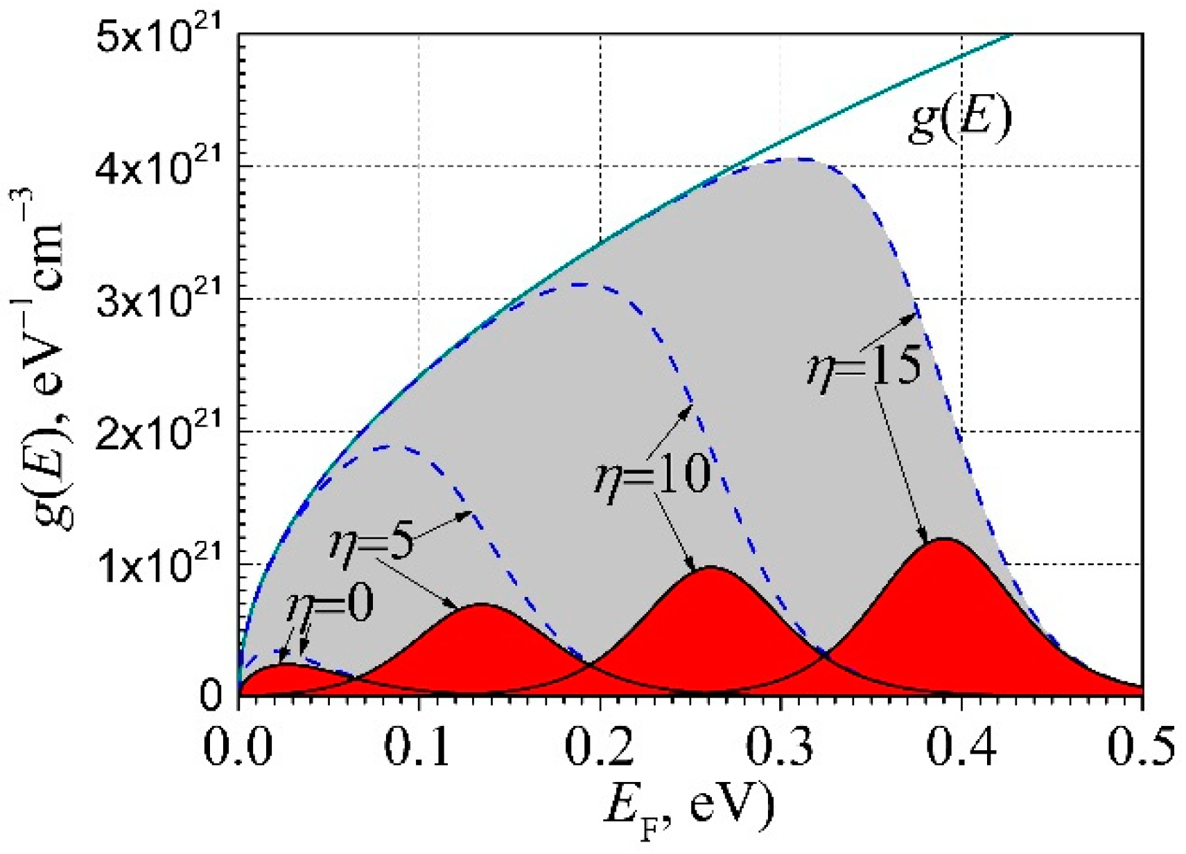
In
Figure 1 there are presented the electron distribution on energy in the conduction band of silicon with degenerate electron gas at various relative Fermi energies
.
It is clearly seen that for highly degenerate electron gas (
η ≥ 5) the effective free RM electron density is many times smaller than the total electron density in the conduction band. In
Figure 2 there is presented the effective free RM electron density dependence on the total electron density in the conduction band of
n-type silicon at room temperature. The effective free RM electron density is equal to the total density of the electrons in the conduction band when the latter is smaller than 10
19 cm
−3 (the classical statistics is valid), but at very high electron density in the conduction band (
n > 10
20 cm
−3, the effective free RM electron density changes slower as
.
2.2. The Free RM Electron Density Dependence on the Phosphorous Doping Level in Silicon
Now let’s see how the total density of electrons in the conduction band depends on the phosphorous doped silicon. Silicon crystallizes in the diamond structure. Each atom forms four covalent bonds, one with each of its nearest neighbors, corresponding to the chemical valence four. When valence-five phosphorous atom is incorporated in the lattice at the site of a silicon atom, the fifth (excess) valence electron of the phosphorous atom is not required for bonding and thus is weakly bounded. The first Bohr radius of the “impurity orbit” is about ten times as large as the lattice constant [
21,
22]. The phosphorous atom ionization energy in silicon is comparable with
kT at room temperature, and this energy level is located 0.045 eV below the conduction band bottom. Considering that phosphorous atoms replace the silicon atoms in the lattice [
23], they did not change the number of elementary cells in the silicon crystal, and at the same time, they did not create additional energy levels in the conduction band. The donor levels are formed as decoupled levels from the conduction band, so the total DOS due to doping yet at high doping levels changes weakly [
20]. It is confirmed by electronic heat measurements of silicon with heavy doping silicon by phosphorous [
24].
At higher donor densities they interact with each other causing an overlap in their wave functions and donor ionization energy decrease and splitting.
A decrease in the phosphorous ionization energy with increase in doping density can be estimated as [
20]
Due to thermal lattice vibration some electrons are excited from phosphorous donor energy levels into the conduction band. In general case, the total excited electron density into conduction band can be estimated by the following expression [
20]:
where
;
;
is the neutral (non-ionized) donor density; for donors
;
; for silicon
cm
−3;
The relative electron density
n/
nd in the conduction band and the Fermi level energy dependences on temperature at three phosphorous donor densities in silicon are presented in
Figure 3. Usually, it is considered that all phosphorous donors are completely ionized at temperatures above the liquid nitrogen temperature.
As it seen from
Figure 3, the requirement that 95% of the phosphorous donors will be ionized at temperatures above the liquid nitrogen temperature is fulfilled only at low (≤10
13 cm
−3) phosphorous donor densities. This ionization level for phosphorous donor density 10
15 cm
−3 is achieved at temperature above 110 K, and for 10
17 cm
−3 only at temperature over 240 K. As it is seen from
Figure 3, only 24% phosphorous donors are ionized at liquid nitrogen temperature. So, a statement that all phosphorous donors are ionized at temperatures over liquid nitrogen temperature should be used with extreme caution. What determines that not all phosphorous donors are ionized at higher densities?
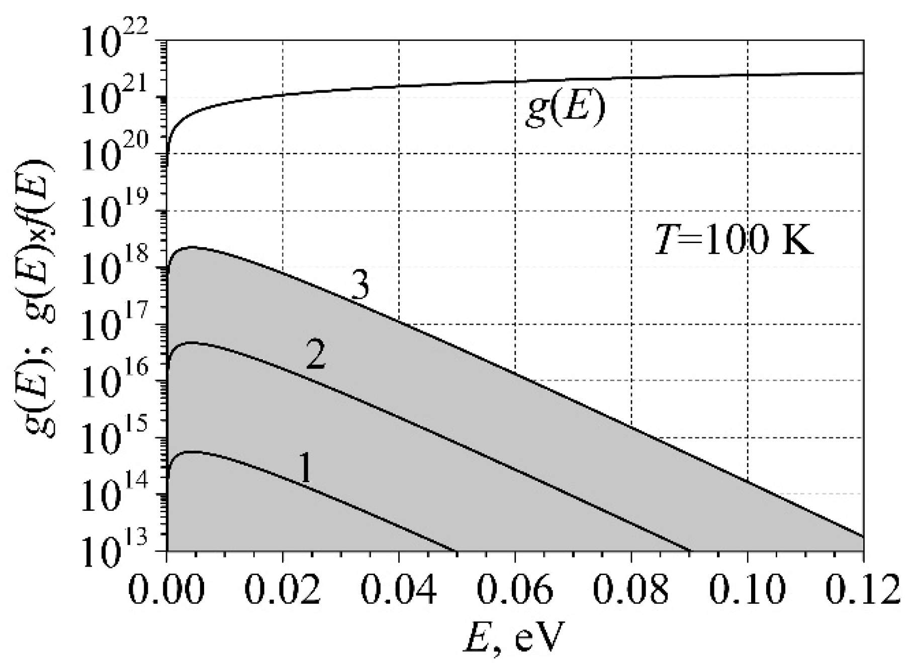
The higher the phosphorous donor density, the lower the relative electron density in the conduction band. The dependence of the conduction band filling by electrons is described by function
f(
E)g(
E), which at
T = 100 K is presented in
Figure 4 for three phosphorous doping densities. At low donor density the electrons fill the energy states near the bottom of the conduction band. The area below the curve 1 for phosphorous doping density 10
13 cm
−3 shows that phosphor donors are completely ionized; the area below the curve 2 for donor density 10
15 cm
−3 shows that about 93% of the phosphor donors are ionized (
Figure 3), and the area below the curve 3 for donor density 10
17 cm
−3 shows that only 47% of the phosphor donors are ionized. At higher phosphorous doping densities some part of donor electrons must be excited to the higher energy levels of conduction band, and at a given temperature not all phosphorous donors are ionized, because the lattice vibration energy is not enough. For complete ionization is needed the higher temperature.
Considering that at room temperature all phosphorous donor excess (fifth) electron energies are located in the conduction band, the density of electrons in the conduction band is equal to the donor doping density:
n =
nd. The ratio between the effective free RM electron density and the total density of electrons in the conduction band of silicon dependence on the phosphorous doping density at room temperature is presented in
Figure 5. Here
In the case of high doping (nd > 1018 cm−3), only the electrons neff described by Equation (1) are free and can randomly move in the silicon crystal, the other part (n-neff) of electrons located by a few kT below the Fermi level energy is bounded with the native phosphorous ion and move around in the central field of the native phosphorous ion. These electrons are not affected by lattice vibrations, and their energy variance is equal to zero. The lattice vibration energy is only sufficient to excite (decouple) the electrons which have energies near the Fermi level energy, and they become free. Thus, not all electrons having energies in the conduction band are free, and not all phosphorous atoms are ionized at high doping level at room temperature. So, the free electron term can be used only for the free RM electrons, the other part (n-neff) of electrons is localized near the native phosphorous ions.
The relative neutral (non-ionized) phosphorous donor density dependence on the donor density is presented in
Figure 5 by dash line. As it is seen, at a doping level of about 10
21 cm
−3 about 90% of phosphorous atoms are not ionized. On the other hand, at doping densities smaller than 10
18 cm
−3 all phosphorous atoms are completely ionized, and produce the free RM electrons, which take part in conduction. The tunneling effect confirms this conclusion: Electrons are tunneling only from energy levels near the Fermi level energy.
2.3. The Free RM Electron Diffusion Coefficient and Drift Mobility Dependences on the Phosphorous Doping Level in Silicon
Considering the Boltzmann kinetic equation, when an external electric strength
E is weak, the current density
j in homogeneous material can be estimated as [
25]
where
v is the free RM electron velocity, and
τ is their relaxation time. Accounting the Equation (2), the Equation (10) can be rewritten as
The calculation and averaging of this Equation can be performed in the following way:
where the Equation (1) for
neff is used. Thus, it is the general expression for conductivity of homogeneous material:
where
D = (1/3) <
v2><τ> is the diffusion coefficient of the free RM electrons. On the other hand, the conductivity can be described as
where
is the drift mobility of the RM electrons. The presented Equations (13) and (14) are valid for all homogeneous materials with any doping level. Moreover, from these Equations also follows that Einstein relation
is valid at any degree of degeneracy of electron gas. There it can be pointed that in many of the published works, it is considered that the Einstein relation is valid only for materials with non-degenerate electron gas, and for degenerate semiconductors they use the so named modified relation [
8,
9,
10,
11,
12,
13,
14,
15]:
where
n is the total density of electrons in the conduction band, and
μ is their mobility. This relation can be written as
where both sides mean the conductivity, but the left side
is the general expression of conductivity (Equation (13)) which is valid at any degree of degeneration of electron gas, while the right side of the Equation (17) is valid only for non-degenerate semiconductors. Thus, the modified relation (16) is not right.
From Equation (15) the drift mobility can be described as:
It is seen that drift mobility in general case depends on the average kinetic energy of the free RM electrons. Here
is the effective mass of the free RM electron. The average kinetic energy of a free RM electron can be estimated as
The dependences of the average kinetic energy and the Fermi level energy on the electron density in conduction band are shown in
Figure 6.
The Fermi level energy has been evaluated from Equation (7). For non-degenerate electron gas (
n < 10
18 cm
−3) the average kinetic energy of the free RM electron is equal to (3/2)
kT, and the drift mobility and conductivity take usual forms of the classical statistics:
So, the Drude electron conductivity model can be applicable only for semiconductors with non-degenerate electron gas but is completely unsuitable for metals and other materials with highly degenerate electron gas. At high doping levels the average kinetic energy increases and approaches the Fermi level energy (
Figure 6), and as a consequence, the drift mobility (Equation (19)) also increases with high doping increasing.
The diffusion coefficient has been evaluated by using Equations (1) and (13), and the data from
Figure 7. The drift mobility of the free RM electrons has been evaluated by Equation (15). The evaluation results are presented in
Figure 8. From comparison the diffusion and the drift mobility on the donor doping level, it is seen that the increase in those parameters at high doping level is caused by the increase in the kinetic energy of the free RM electrons (
Figure 6).
2.4. The Hall Effect in Phosphorous Doped Silicon at Any Doping Level
Let’s compare the obtained drift mobility results with that from the Hall effect measurement. The Hall coefficient
RH, when the direct current flows only along
x direction, and magnetic field is directed along
z axis, is determined from the following relation:
where
jx is the direct current density in
x direction,
Bz is the magnetic flux density in
z direction, and
Ey =
EH =
UH/
w (here
UH is the Hall voltage) is the originated electric field strength in
y direction in the material plate with dimensions
d ×
w ×
l (thickness × width × length),
Ex =
Ux/
l (here
Ux is the applied voltage in
x direction),
σ is the conductivity of the sample material with one type of free charge carriers.
Instead of the Hall coefficient, the Hall effect is sometimes characterized by the Hall angle
φ. For small direct current density and weak magnetic field, the Hall angle is described as
On the other hand, the Hall angle can be expressed by cyclotron angular frequency
ωc =
qBz/
m* [
27]:
where
is the Hall factor, which depends on the charge carrier scattering mechanism, but for highly degenerated electron gas it is equal to 1. It is notable that
ωc does not depend on the radius and velocity, and therefore, is independent of the particle kinetic energy. All particles with the same charge-to-mass ratio rotate in magnetic field with the same cyclotron angular frequency, i.e., electrons with the same effective mass moving with the thermal velocity in material with non-degenerate electron gas, and electrons moving with Fermi velocity in metals have the same cyclotron angular frequency. From Equations (23)–(25) follows that
Considering that quantity
μH has a similar dimension expression as for mobility of charge carriers in semiconductors with non-degenerate electron gas, this quantity is named as Hall mobility. The Equation (26) is valid at any degeneration degree of electron gas with one type of the free RM charge carriers. The Hall coefficient RH has a negative sign for electrons and positive sign for holes. Note: If one compensates
Ey by external bias source to zero, as it is usually done in measurement of the Hall voltage, it has no influence on both the cyclotron frequency and drift mobility of the free charge carriers of the material. A comparison of the Hall and the drift mobilities are presented in
Figure 9. It is seen that drift mobility at high donor doping can many times exceed the Hall mobility. From this comparison at
n < 10
18 cm
−3 we can simply find the Hall factor
.
In general case, the conductivity of homogeneous material with one type of free charge carriers by using Equations (14) and (19) can be described as
Then from Equations (26) and (27) the Hall coefficient can be expressed by such general relation:
which is valid at any degree of degeneration of electron gas with one type of free charge carriers. Here the parameter
= <
E>/[(3/2)
kT] shows how many times the free RM electron kinetic energy is higher than the thermal energy. The effective free RM electron density dependence on the total electron density in conduction band of donor-doped silicon at room temperature is presented in
Figure 2. For silicon with non-degenerate electron gas
, and drift mobility can be described as
and the Hall coefficient as
Therefore, the Hall coefficient is defined by the free electron density in conduction band only for non-degenerate silicon (n < 1018 cm−3 at room temperature). At high donor doping for estimation of the drift mobility and the Hall coefficient one must use the general Equations (19) and (28), respectively.
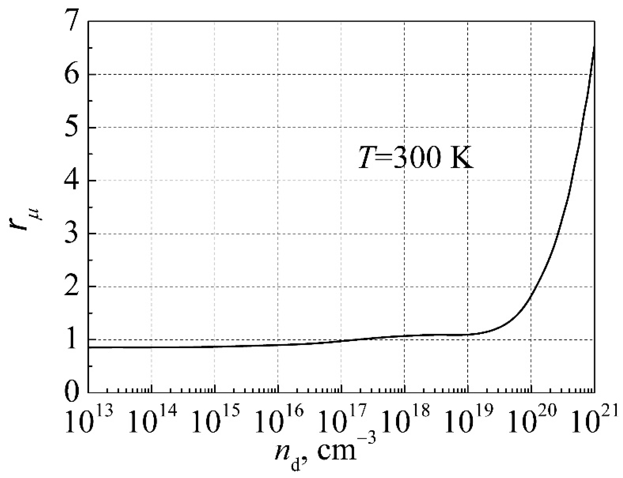
It is worthwhile to introduce a new factor: the drift mobility factor
which reflects the ratio between the drift and Hall mobilities
. The mobility factor at
n < 10
18 cm
−3 , but at higher density
n = <
E>/[(3/2)
kT]. The mobility factor dependence on the phosphorous donor density in silicon at room temperature is presented in
Figure 10. It is seen that the drift mobility at very high donor densities can be about six times larger than the Hall mobility.
2.5. The Plasma Frequency of the Free RM Electrons in Silicon
Alternate current conductivity
usually is described in the following form [
19]:
The relaxation time
τ of the free RM electrons by using Hall mobility data dependence on the donor doping density in silicon at room temperature can be estimated as
where
nd is in cm
−3. The relative permittivity
for
can be approximated as
where
is plasma oscillation frequency:
Accounting the general Equation (27) for conductivity σ, the plasma frequency can be expressed as
In the case of non-degenerate electron gas,
, and
, the plasma frequency can be described in the usual form [
19]:
For highly degenerate electron gas, the plasma frequency is estimated as
Though the Equation (37) can be expressed in the form of the Equation (36), but it does not mean that all electrons from conduction band at high doping take part in collective oscillations. It is not true because the applied alternate electric field can only change the energy of the free RM electrons, which energy is located near the Fermi level energy, while the other part of electrons (n-neff) which are coupled with the phosphorous ions does not take part both in the conductivity and in the plasma oscillations.


