Review

X-ray Based in Situ Investigation of Silicon Growth Mechanism Dynamics—Application to Grain and Defect Formation

1
Aix Marseille Univ, Université de Toulon, CNRS, IM2NP, 13397 Marseille, France
2
Arts et Metiers Institute of Technology, MSMP, HESAM Université, F-13617 Aix-en-Provence, France
3
ESRF—The European Synchrotron, CS40220, 38043 Grenoble CEDEX 9, France
*
Author to whom correspondence should be addressed.
Crystals 2020, 10(7), 555; https://doi.org/10.3390/cryst10070555
Submission received: 3 June 2020 / Revised: 25 June 2020 / Accepted: 27 June 2020 / Published: 30 June 2020
(This article belongs to the Special Issue Growth and Evaluation of Crystalline Silicon (Volume II))

Abstract

:
To control the final grain structure and the density of structural crystalline defects in silicon (Si) ingots is still a main issue for Si used in photovoltaic solar cells. It concerns both innovative and conventional fabrication processes. Due to the dynamic essence of the phenomena and to the coupling of mechanisms at different scales, the post-mortem study of the solidified ingots gives limited results. In the past years, we developed an original system named GaTSBI for Growth at high Temperature observed by Synchrotron Beam Imaging, to investigate in situ the mechanisms involved during solidification. X-ray radiography and X-ray Bragg diffraction imaging (topography) are combined and implemented together with the running of a high temperature (up to 2073 K) solidification furnace. The experiments are conducted at the European Synchrotron Radiation Facility (ESRF). Both imaging techniques provide in situ and real time information during growth on the morphology and kinetics of the solid/liquid (S/L) interface, as well as on the deformation of the crystal structure and on the dynamics of structural defects including dislocations. Essential features of twinning, grain nucleation, competition, strain building, and dislocations during Si solidification are characterized and allow a deeper understanding of the fundamental mechanisms of its growth.

1. Introduction

Current research on crystalline Si used for photovoltaic solar panels focuses on several key targets from silicon purification to cell manufacturing including the silicon ingot fabrication process step. Several alternative methods are proposed to optimize the Si growth process to increase the production yield while reducing the costs. However, this cannot be done at the expense of the crystalline quality of the final ingot as the performance of the solar cells is directly related to it. Three main methods aim at mastering the initial grain nucleation and defect generation from the first stage of solidification: the dendritic casting method [1,2], the cast mono solidification (cm-Si) [3,4,5], and the high performance multi-crystalline silicon (HP mc-Si) [6]. HP mc-Si and cm-Si techniques are both used in the industry and allow producing ingots with a lower dislocation density compared to the conventional mc-Si while allowing the use of low-cost casting solidification methods. In the case of cm-Si, a pavement of monocrystalline seeds is placed on the bottom of the crucible in order to take up the initial orientation of the seed [3]. However, cm-Si efficiencies are still limited due to the presence of structural defects such as parasitic grain nucleation on the walls of the crucible [4,7], twin formation and more importantly, dislocations. The latter can be either arranged in cellular patterns, in the entire cm-Si ingot and are known as background dislocations [8] or generated on the top of the seeds [9,10], at their junctions on precipitates [10] and propagate vertically along the growth direction [9,11,12,13,14,15,16] generating the formation of sub-grain boundaries. HP mc-Si technique is based on a very different approach aiming at obtaining small-size and uniform grains at the initial stage of solidification with random angle and coherent grain boundaries [6,17]. This results in low density of dislocation clusters thanks to blocking mechanisms by which dislocations that nucleate at the beginning of the crystallization process cannot propagate further along the growth of the ingot. Recent work by Stokkan et al. [17] highlighted the necessity to control the first nucleation events to improve the crystalline quality. It is worth noting that in the other main process in the market, Czokralski (Cz), which aims at the of the fabrication of monocrystalline ingots the issue of dislocations and structural defects remains a main concern especially when one wants to improve the method (higher volumes, faster process, reusable crucibles and seeds, etc.) [18,19].
Grain boundaries and dislocations can severely limit the conversion efficiency of solar cells by reducing the minority carrier lifetime [20,21,22,23]. Dislocations remain one of the most important efficiency limiting defects in Si solar cells, because they can act as preferential segregation sites for impurities, ultimately reducing the carrier lifetime [11,16,24,25,26]. At a higher scale, sub-grain boundaries and grain boundaries of high planar mismatch can be more detrimental than high symmetry grain boundaries such as symmetric coincidence site lattice (CSL) twin boundaries, also due to decoration by impurities [27]. Various studies show that the crystalline quality of an ingot in general and the twin relationship between the grains in particular can have a significant impact on the photoelectric properties [27,28,29]. Moreover, although it has been shown that perfect symmetric ∑3 twins have no major impact on the photovoltaic properties, the repetition of twinning has important consequences for the final grain structure and distribution of crystallographic orientations [30,31]. The importance of twinning in the development of the grain structure has been highlighted for very different solidification processes including directional mc-Si solidification [32] and ribbon growth [33]. Another issue is to control and lower the density of strained regions of the crystal structure that can be at the origin of dislocation emission during growth or subsequent cooling down and solar cell fabrication processes. Recent molecular dynamics simulations of silicon growth highlighted the interrelation between strain field, dislocation generation relatively to the growth direction, and twin nucleation [34]. The control of the formation of structural defects is thus motivated by their direct impact on the PV properties. Such a control is only possible if a thorough understanding of the crystal growth mechanism is achieved. The understanding of the development of the structural defects during growth is limited by the difficulty of accessing, from the ex situ study of the solidified ingots, to the history of defect formation and interrelation. Moreover, these structural defects cover by essence a large scale range (from dislocations to grains).
To answer these issues and key points, benchmark experiments have been proposed to investigate the growth from silicon melt in situ. Characterization of the solidification of an undercooled levitated silicon droplet was performed using an X-ray diffractometer and by recording the droplet surface image using a high-speed video camera [35]. The in situ solidification behavior of Si droplets on silicon wafers was also characterized using IR thermal imaging [36]. Fujiwara et al. [2,37,38,39,40,41] use a confocal scanning laser microscope to carry out in situ observations of crystal growth from silicon melt by providing live images of solid–liquid interface features and of the growth of grains. With this method, a detailed investigation of the Si microstructure during growth has been carried out. X-ray Bragg diffraction imaging (topography) is also used to characterize crystalline defects [26]. More information and explanation on this technique will be given in the following as this is a method of choice to characterize crystalline defects that we use in our experiments. It is worth mentioning the pioneer work of Pr. Chikawa [42,43] who conducted in situ X-ray topography during melting and solidification of silicon.
Starting from the considerations that in situ characterization of silicon growth constitutes an invaluable tool to understand the crystal growth phenomena and the formation of structural defects, we implemented in situ X-ray imaging during the solidification of silicon. The GaTSBI (Growth at high Temperature observed by Synchrotron Beam Imaging) tool was developed to fulfil this objective. This present paper is a review paper of our major results concerning the formation of grains, twinning, and competition [44,45,46,47,48,49,50,51,52,53] using advanced in situ and complementary ex situ characterization methods. In situ X-ray imaging and methods are described in detail. Our results concerning dislocations and the effect of impurities are not presented in detail here. Results concerning the effect of Cu, C, and O impurities can be found in [53].

2. Materials and Methods

2.1. GaTSBI Tool

GaTSBI is a unique device with which the solidification processes can be characterized in real time during growth. It is a specially designed instrument composed of a high temperature (up to 2073 K) directional solidification (DS) furnace employed in conjunction with synchrotron radiation X-ray imaging techniques (Bragg diffraction imaging—topography and radiography).

2.1.1. Directional Solidification Furnace

The DS furnace is based on two heating graphite resistors that are inside a vacuum chamber under dynamic vacuum (≈10−6 mbar). The powers of the heating resistors are regulated by the external controller of the DS furnace. The control loop uses the temperature values measured by pyrometers pointing on the heaters.
The typical sequence used in our experiments concerning silicon solidification is the following:
  • Step 1—Preheating: the silicon sample cut inside ingots of different origins is heated by applying the same temperature to the bottom and top resistances of the furnace (isotherm conditions) up to 1373 K.
  • Step 2—Temperature gradient: a vertical temperature gradient is applied by imposing a controlled temperature difference between both heaters. The same temperature gradient is maintained until step 5.
  • Step 3—Partial melting: the sample is partially melted (Si melting temperature: 1687 K). This is monitored by imaging during the heating phase. A seed crystal, preserving the initial orientation of the sample, is kept within the field of view of the X-ray imaging.
  • Step 4—Solidification: both heaters are cooled at the same controlled cooling rate until the region of the silicon sample observed within the field of view is fully solidified. The same cooling rate is applied on both heaters to maintain a constant temperature gradient during solidification. In some particular cases, not reported in this manuscript, solidification is conducted by pulling the sample downwards. In both cases, the solidification is directional in the upward direction due to the imposed vertical temperature gradient.
  • In some experiments, a new cycle is started again from step 3.
  • Step 5—Controlled cooling down: the sample is cooled down until 923 K by applying cooling rates of −13 and −10.4 K/min to the top and bottom heaters, respectively.
  • Step 6—Cooling down to room temperature: free cooling down takes place from 923 K as temperatures below this value cannot be controlled by design of the furnace.

2.1.2. Crucible Assembly

Two thin pyrolytic boron nitride (BN) plates serve as crucible material. One of the BN plates has a mechanically machined slot with the dimensions of the samples. The typical sample dimensions are as follows: length 40 mm, width 6–8 mm, and thickness about 0.3 mm. The front and back sides of the sample are in contact with the crucible walls. The crucible assembly can be seen for example in Figure 1b of Reference [45]. The two BN plates are held together by two Molybdenum clips so that it applies a pressure on the main surfaces of the samples. In a further step, the silicon sample housed in the BN crucible, is introduced inside the DS furnace.

2.1.3. Origin of the Silicon Samples

The initial monocrystalline Si samples are cut from double side mechano-chemically polished intrinsic (resistivity beyond 5000 Ω.cm) float-zone (FZ) wafers with a diameter of 50.8 mm, or from conventional Cz industrial ingots (typical oxygen concentration: 0.5–1 × 10¹⁸ at/cm3). The FZ samples provided by SIL’TRONIX Silicon Technologies are produced with 9N purity by the float-zone technique and contain no visible dislocations at the beginning of the experiments. Oxygen and carbon concentrations are below <1015 at cm−3 and metallic impurity contamination is limited to 1011 at/cm−3.

2.1.4. X-Ray Imaging

The GaTSBI set-up is not only a DS device but is specifically designed to allow X-rays to cross the furnace windows and elements up to the sample without deleterious absorption and diffraction of the incoming X-rays. The beam crosses the entry and exit vacuum chamber windows that are made out of 0.5 mm thick aluminum. Additional vitreous carbon plates are positioned in the beam path serving as insulation of the furnace. As a consequence, a high photon flux is needed to ensure good quality imaging. This is one of the reasons, although not exclusive why the experiments are conducted using synchrotron X-ray generated at the European Synchrotron Radiation Facility.
A schematic drawing of the general imaging assembly can be found for example in Figure 1a in Reference [45]. During the experiments, the sample inside the DS furnace is constantly illuminated by the X-ray synchrotron polychromatic beam, which avoids variations of the heat load due to the beam. Indeed, the polychromatic beam creates heat load which is minimized with filters introduced in the beam before reaching the DS furnace. A compromise between minimized heat load and sufficient photon flux needs to be achieved resulting in the utilization of Al filters between 0.5 and 0.7 mm in our experiments. On the one hand, a sufficient photon flux level is assessed qualitatively by checking that the solid–liquid interface can be characterized with a counting time not higher than 1 s which is required to be able to follow its dynamic evolution during solidification. On the other hand, variations of the heat load need to be minimized for two reasons: it is sufficient to modify the thermal field inside the sample, it modifies the behavior of the crystals used in the post-monochromator that will be described in the following.
Two imaging techniques, X-ray radiography and X-ray Bragg diffraction imaging (topography), are used during the steps described in Section 2.1 (heating, solidification, and cooling down of the samples). Both imaging techniques are non-destructive.

2.1.5. X-Ray Radiography

In the X-ray radiography mode, the direct beam passing through the sample is used to record images of the growing solid–liquid interface. A polychromatic beam is needed for the diffraction imaging mode, whereas a monochromatic beam is needed in the case of X-ray radiography to increase the legibility of the images. First, the polychromatic direct X-ray beam goes through the sample and exits the furnace vacuum chamber. The polychromatic direct beam is then turned monochromatic at a target energy, empirically determined as explained in the following, using a vertically diffracting Si (111) double-crystal monochromator. Finally, images are recorded using a camera equipped with a scintillator to interface X-rays with the camera matrix detector.
X-ray attenuation contrast is the dominating imaging modality used in the frame of this work. Considering the use of synchrotron light sources, an additional modality present is related to the refraction at interfaces, frequently termed propagation-based X-ray phase contrast [54,55]. Due to the rather coarse pixel sizes used and to the relatively short distance between sample and detector, the effect of phase contrast is not pronounced in the images shown in this work and therefore only mentioned for the sake of completeness. Thus, the contrast in X-ray imaging radiographs shown here is mainly due to the differential absorption of the different sample regions. The Beer–Lambert law determines the absorption of a material (Equation (1)). Incident monochromatic beam intensity is exponentially attenuated as a function of the thickness, of the nature of the sample and of other materials crossed by the incident beam:
I t = I 0 e µ i ( T , C ) . l
where It is the transmitted intensity, I0 is the incident intensity, µi is the linear absorption coefficient (in m−1), which depends on the temperature T and on the composition C while l is the thickness. The linear absorption coefficient is a function of the density of the material.
As the absorption of other materials crossed by the beam is constant, the only contribution to the image contrast comes from the sample. In the case of a pure material such as silicon, a difference in transmission, and therefore a contrast in the images, is expected only from the density difference between the solid (2.33 g/cm3) and the liquid (2.56 g/cm3) close to the melting temperature Tm. This density difference is only 9%. The use of monochromatic light is essential to exploit the weak attenuation contrast originating from this density difference between the solid and the liquid silicon phases in the radiography images. The choice of the monochromatic energy used for X-ray radiography is based on a compromise between an acceptable transmission and a contrast allowing to reveal the solid–liquid interface features. During our experiments, it was empirically determined that an energy of 17.5 keV must be used, which corresponds to a transmission of 63% of the liquid phase. However, the contrast between the solid and liquid phase is then only about 4%. Due to the limited density difference and the compromise in energy, the solid–liquid interface is hardly distinguishable on the raw images oppositely to the case of alloys for which a higher density difference is obtained because of the presence of several phases and of solute [56]. In addition, the legibility of the images is considerably affected by the unavoidable non-uniform profile of the X-ray beam and by the surface inhomogeneity of the silicon crystals in the post-monochromator. As a consequence, image processing is absolutely needed.
The image processing is based on the principle of pixel by pixel division and is performed using the ImageJ software [57]. By dividing two images recorded at different times, the areas that remain in the same state (liquid or solid) have the same transmission and corresponding pixel values in the images, thus the result of the division is equal to 1. As the liquid transmission is lower than the solid transmission, zones that change from liquid to solid appear in lighter grey (the result of the division is lower than 1), and zones that change from solid to liquid appear in darker grey (the result of the division is higher than 1).
Two types of treatment are used:
  • Division by the first image taken after cooling starts:
For this treatment, all images of the solidification sequence are divided by a single reference image recorded just after applying the cooling rate. A typical image resulting from this treatment is shown in Figure 1a, α, β, and δ indicate the region of the regrown interface, the fully solid and liquid regions, respectively. A light grey area is observed above the fully solid zone (γ in Figure 1a). This area corresponds to a zone constituted of solid and liquid that exists within the thickness of the sample at the level of the solid–liquid interface. This is first due to the fact that the images correspond to a projection of the sample volume hit by the beam and second to the orientation of the solid–liquid interface which is not necessarily parallel to the incident beam. An illustration of a possible solid–liquid interface side view configuration is depicted in the sketch in Figure 1b. At the level of the solid–liquid interface region, the beam goes through both solid and liquid regions which explains the grey level neither corresponding to a fully solid volume nor to a fully liquid volume.
This treatment allows following the evolution of the solid–liquid interface during growth. Dynamic features can be observed, and the growth velocity of the solidification front can be measured.
  • Division of two successive images:
For this treatment, each image is divided by the previous one or by an image separated from the current one by a few images only (Figure 1c). In this case, the resulting image is less prone to noise and artefact variations in beam intensity with time as for the first treatment. Then, sharper contours are obtained, revealing more details of the solid–liquid interface as can be seen in the close-up in Figure 1c which shows more clearly the same grain boundary groove (close-up in Figure 1a). The morphology of the interface and of the grain boundary grooves can thus be studied in detail.
The radiography technique allows observing the growth of the interface, measuring the growth velocities, studying the evolution of grain boundary grooves, and the appearance of facets and twins. It provides a non-deformed image of the solid–liquid interface and of the sample. The volume projection effect needs to be taken into account for quantitative measurements (e.g., for the measurements of the facet normal growth rate discussed in Section 3.1 and described in more detail in [48]).
In the experiments presented in the following, the X-ray radiography images are recorded on detectors based on the association of a scintillator to convert X-rays in visible light and of a CCD or CMOS camera detector [58]. An optics giving a good compromise between a large field of view encompassing the whole sample width, a solidification height of about 10 mm, and a sufficient spatial resolution is used. More precisely, two detectors were used. First, a CCD camera developed at the ESRF named FReLoN (Fast Readout Low-Noise) with 2048 × 2048 pixels was used and coupled with an optics giving a 5.8 μm pixel size and a 11.9 × 11.9 mm2 field of view. In our most recent experiments, a detector (sCMOS lens-coupled to a LuAG scintillator) 2048 × 2048 pixels with a nominal pixel size of 6.5 µm2 and a 16 bit dynamic range was used.
Radiography images are generally recorded every 3 s with an exposure time of 1 s which is a sufficient time-resolution to be able to characterize solidification.

2.1.6. X-Ray Bragg Diffraction Imaging—Topography

X-ray Bragg diffraction imaging (X-ray topography) is the complementary and essential non-destructive technique used to characterize the grown crystal quality during the same experiment. When the polychromatic beam illuminates the silicon sample installed inside the solidification furnace, diffraction occurs according to Bragg’s law, generating a Laue diffraction pattern in addition to the direct beam exploited for X-ray radiography. The Laue diffraction pattern is constituted of several diffraction spots related to specific lattice planes.
The transmission mode is used i.e., the incident beam is transmitted through the sample and the diffracted beams expose a detector that is placed after the sample. Transmission mode is the only possible one in our experiments as the sample is installed inside the vacuum chamber containing the furnace. The use of a polychromatic beam allows collecting multiple spots from multiple grains in a single exposure as well as several spots corresponding to different crystallographic planes {hkl} of a single grain.
Each spot provides an image of the crystal generated by the beam diffracted by the {hkl} plane family of a grain, called topograph [59]. These Bragg spots are then characterized by the hkl Miller indices of the diffracting plane and by the projection of the diffraction vector g (reciprocal lattice vector), indicating the orientation of the spot with respect to the position of the direct beam. This technique can obviously give information on the crystallographic orientations of the grains considering the relative position of the diffraction spots, but its major output concerns the internal structure of the individual spots as they contain information on misorientations, strain, and by extension on the presence of structural defects in general. Indeed, this is a powerful technique that can be used for the visualization of defects (dislocations, twins, domain walls, inclusions, impurity distribution) present in the crystal volume as it records their long-range distortion fields and/or the strain fields associated with a macroscopic crystal deformation. However, one drawback of the technique is the complex analysis of the obtained images which are distorted images of the crystals. The origin of the contrast observed in the images is briefly explained here, the reader is directed to several references for more details [9,59,60,61,62].
Due to the small beam divergence of the incoming synchrotron X-ray beam and to its large size, the whole width of the samples can be illuminated providing images exhibiting a minimum geometrical deformation effect. In our case, the diffracting volume corresponds to the width of the sample × the height of the field of view (generally 10 mm) × the thickness of the sample. It is worth noting that contrarily to more classical diffraction configurations, a limited number of diffraction spots can be collected during our experiments. This is due to both the distance between the sample and the diffraction pattern detector and the detector size. Indeed, although distance minimization is always possible to some extent, some hard limits are imposed by the DS furnace vacuum chamber needed to run solidification experiments. It explains why only a few diffraction spots are recorded on the films when they are used to record the diffraction pattern.
A few mechanisms are responsible for the contrast and intensity on the X-ray topographs we recorded. They are structure factor contrast, orientation contrast, and the so-called “direct image” mechanism. All of them derive from diffraction theory and Bragg’s law as explained for example in [63] and are evidenced in Figure 2; Figure 3.

2.2. Orientation Contrast

A particularly clear illustration of the orientation contrast is given in the presence of twins observed in our experiments (Figure 2 and Figure 3) [46,50].
Indeed, in the case of twinning during growth, the diffraction images are very different depending on the diffraction spots as can be seen in Figure 2. A typical hatched aspect is observed for the diffraction spots corresponding to some {hkl} family planes as can be seen in Figure 2b (e.g., α, β, and χ). The diffraction spot χ 2 ¯ 20 shows a diffraction spot corresponding to {hkl} family planes which are not common with twinned grains that developed on both right- and left-hand sides of the sample (Figure 2c). The complementary image corresponding to the twinned grains on the left (Figure 2b β) is found at another position of the diffraction pattern, whereas the diffraction spot α 1 ¯ 1 1 ¯ includes the diffraction patterns of the common family planes of the central main grain and of the twinned grains on the left (Figure 2d). This is a particularly important element to be kept in mind when analyzing the topographs. Indeed, the observation of a single diffraction spot can be misleading. This is one of the reasons why several diffraction spots must be analyzed to be able to conclude.
Orientation contrast can also be produced, for instance when the sample displays sub-grain boundaries. For a monochromatic beam, the region corresponding to a {hkl} plane family is imaged at a position given by the Bragg’s law. Regions of different crystallographic orientations are not seen simultaneously on the diffraction image and appear as non-illuminated (white) zones. When a polychromatic beam is used, the misoriented regions are all in diffraction position simultaneously, but for different wavelengths. The images diffracted by neighboring sub-grains can exhibit a contrast associated with geometrical local superimpositions or separations of the diffracted beams on the topographs, according to the dimensions of the misoriented zone and to the value of the misorientation.
Additionally, crystalline defects such as precipitates, dislocations, and impurities, act on the diffraction process through their associated effective misorientation angle variation δ θ m ( r ) , which can be approximated by Equation (2) [60,62]:
δ θ m ( r ) = δ d d ( r ) t a n θ B ± δ θ ( r )
where θB is the Bragg angle, δ d d ( r ) is the local relative change of the lattice parameter and δ θ ( r ) , the local change in crystallographic orientation. The double sign has to be chosen to take into account the effect of the deformation on the Bragg angle (decrease or increase of its value). This effective misorientation corresponds to the strain field generated by the defect, which is at the origin of Bragg diffraction of components of the incident beam that do not participate in the diffraction for the perfect crystal matrix [45,61]. This is the “direct image” mechanism that leads, in the X-ray low absorption case we are concerned with, to supplementary diffracted intensity associated to distorted regions. Andrew Lang developed this technique and revealed dislocations in silicon in his pioneer work [59]. The diffraction imaging technique was also used by Oriwol et al. [26] to study dislocations and the formation of sub-grain boundaries ex situ in Si ingots. Indeed, diffraction imaging applied to silicon crystals have proven to give unique insights into the evolution of dislocations [64,65] and cracks [66]. As can be understood from the above, one of the main advantages of diffraction imaging is that it can reveal low scale structural defects like dislocations on wide field images encompassing complete crystals as shown for example for diamonds by Burns et al. [61] and for Si [45,52,67].
An illustration is shown in Figure 3c. In this topograph corresponding to the 1 1 ¯ 1 diffraction spot and recorded during the solidification from a silicon FZ seed (orientation Figure 3a), black contrasts revealing deformation of the crystal structure are present at several places. Moreover, the deformation due to single dislocations can be clearly revealed in the seed and above the seed–regrown interface.
Importantly, if the strain field created around a defect is related to particular crystallographic orientations, it is not visible in all diffraction spot images (topographs). Indeed, if the displacement vector is perpendicular to the diffraction vector, the defect is not visible on the topograph. This is the case of dislocations whose image is extinct for the diffraction spots corresponding to diffraction vectors perpendicular to the Burgers vectors as also seen in TEM investigations [68,69]. On the one hand, this means that the absence of a dislocation strain field on a single diffraction spot does not mean that no dislocations are present. Depending on the dislocation character, at least two diffraction spots with different diffraction vectors perpendicular to each other must be analyzed before being able to conclude on the presence or not of dislocations. On the other hand, extinction is a powerful method to retrieve the Burgers vector direction as explained in detail for example in [70].

2.3. Dynamic Evolution

Another main originality of the experimental configuration we use is that several Laue patterns or topographs are recorded during a solidification experiment [45,46,71]. Then, it is possible to obtain sequences showing the evolution with time of the Laue pattern and of the topographs during the development of the grains. Such sequences allow a better understanding of the competition between the grains and of the occurrence of the twinning phenomenon. At the same time, the dynamics of the formation and evolution of defects as dislocations is followed during growth. The study of the growth of individual grains is then possible, along with the development of strain fields produced in the crystal structure by the structural defects. The combination of both imaging techniques and of the DS furnace provides complementary information on the dynamics of crystal growth and competition and on the deformation of the crystal structure.
Up to 2018, both in situ and real time X-ray imaging techniques, X-ray radiography and Bragg diffraction imaging (topography), were used alternately during growth. In this configuration, the different diffraction spots are collected on photographic films positioned after the furnace regularly during the experiment thanks to a specially designed device. X-ray diffracted beams are successively recorded on X-ray sensitive films (AGFA Structurix D3-SC, 17.6 × 12.5 cm2) positioned at a distance about 300 mm from the sample. The exposure time used to record the diffraction patterns is usually 0.5 s. In this configuration, radiographs and topographs are thus recorded alternately.
In 2018, we implemented together with the ESRF ID19 team a solution to record simultaneously radiographs and diffraction images (topographs). In this configuration, a scientific CMOS camera lens-coupled to a LuAG scintillator (commercial Ce-doped Lu3Al5O12, Crytur company—Turnov, Czech Republic) is used to record the images of one of the diffraction spots (topograph). The camera has 2048 × 2048 pixels with a nominal pixel size of 6.5 µm2 and a dynamic range of 16 bit. It is coupled with a × 1.5 optic to decrease the pixel size to 4.3 µm2. In this new configuration, images recorded from both modes are fully synchronized. The image acquisition rate is of two frames per second in experiments reported in [52] which is sufficient to follow the solidification front of the samples. The choice of the diffraction vector of the recorded spots and the alignment of the camera with respect to the sample face is an important aspect because it influences the information that can be revealed from the recorded topographs. Ideally a spot with a high intensity induced by the crystal plane structure factor should be chosen to better reveal defects. A detailed description of the equipment and imaging methods and configurations (alternate or simultaneous recording) can also be found in our previous publications [49,50,52].

2.4. Ex Situ Complementary Investigations

After the last melting–solidification cycle, the samples are cooled down to room temperature and removed from the GaTSBI furnace. Ex situ electron backscatter diffraction (EBSD) measurements are performed using a FEG-SEM JEOL JSM 7001F equipped with a HKL Nordlys camera after mirror polishing down to 1 µm with diamond paste. A step size of either 7 or 0.7 μm is used depending on the studied area. In order to depict the three-dimensional orientation of the crystals in the sample, inverse pole figure (IPF) orientation maps are generated with respect to the three space directions: normal to the sample surface (z), transverse direction (y), and in the growth direction (x). Moreover, the coincidence site lattice map (CSL) is reconstructed to evidence the grain boundaries separating grains with a specific crystallographic relationship. In this paper, Σ3 <111> (red color in the maps), Σ9 <110> (blue), and Σ27a <110> (yellow) twin boundaries labelling refer to rotations around the <h k l> axis that satisfy the misorientation ranges given by the Brandon criterion, (60 ± 8.66)°, (38.94 ± 5)° and (31.58 ± 2.89)°, respectively. Additionally, the grain orientation spread (GOS) map is extracted as well from the EBSD results. The GOS map is constructed by calculating the difference between the orientation of each pixel in the grain and of the grain average orientation to evidence the distorted areas within a grain structure. A color code is used to depict the grains without deformation (perfect Si crystal appears in blue) and having an average crystal structure deformation (red color for the highest deformation).

3. Results and Discussion

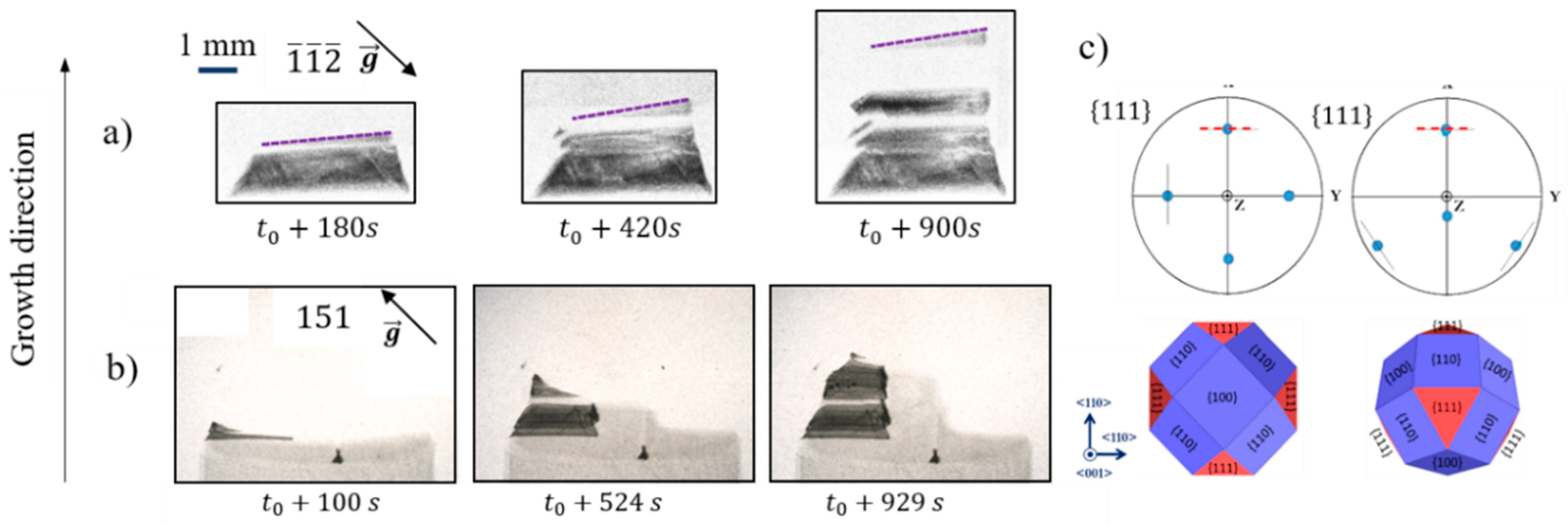
3.1. {111} Facet Growth and Undercooling

Theoretical models of the {111} facet growth laws exist [72,73] and are related to the undercooling at the level of the {111} facets. However, the orders of magnitude of the undercooling values for the corresponding laws are very different, so that experimental validation is needed. Moreover, directional solidification is widely used for the fabrication of multi-crystalline ingots so that the knowledge of {111} facet dynamics needs to be known during DS. Moreover, it constitutes a critical building block to develop predictive and quantitative models [74,75,76]. At last, the presence of {111} facets at the solid–liquid interface leads to the occurrence of twinning ultimately competing with the central grain growing from the seed as will be discussed in the following. It is thus essential to understand their mechanism of formation and the undercooling at their level which gives conditions for twin nucleation. Our main objective was, thus, to determine the contribution of the undercooling of the {111} facets at the solid–liquid interface during Si directional solidification. {111} facet growth laws are derived and then compared with theoretical growth models reported in the literature.
At the level of the solid–liquid interface, {111} facets appear at the sample edges and in grain boundary grooves. Grain boundary grooves are formed due to the encounter between a grain boundary and the solid–liquid interface [77]. From the theory [78], grain boundary grooves can be either facetted/facetted, facetted/rough, or rough/rough depending on the crystallographic orientation of the adjacent grains. Experimentally, we are able to characterize facetted/rough and facetted/facetted grain boundary grooves [48,51] with a large prevalence for the facetted/facetted configuration. However, conclusions concerning the predominance of one or the other grain boundary groove type cannot be drawn from these observations as rough/rough grain boundary grooves are expected to correspond to lower undercoolings compared to facetted/facetted ones and thus to smaller depth that can then fall below the spatial resolution used in these experiments.
Whatever conditions, facets observed in our experiments are always {111} facets as foreseen in silicon [79]. It was checked by determining the crystallographic orientation of the grains and their relative {111} facet orientation. In order to determine {111} facet growth laws, the facetted/facetted grain boundary grooves observed at the solid–liquid interface (e.g., in Figure 1 and Figure 4) were geometrically characterized by their angle and depth [80]. The geometrical parameters of the grain boundary grooves can be measured directly on the radiography images collected during solidification (Figure 1 and Figure 4). The kinetic parameters, growth velocity of the interface, and normal growth velocity of the groove facets, are also measured thanks to the time-resolved observation of the solid–liquid interface evolution.
When comparing the growth rate of the global solid–liquid interface to the {111} facet growth rates, it appears first that the growth rates of the {111} facets both inside the grooves and at the edges are smaller than the one of the global solid–liquid interface. This is expected because of the slower kinetics of the {111} planes compared to the other crystallographic orientations so that they are lagging behind other growing orientations and generally behind the global solid–liquid interface [47]. A major consequence is that the undercooling is higher in the groove and at the level of the edge facets compared to the undercooling at the level of the global solid–liquid interface. This favors nucleation events inside grooves and at the edge facets that are indeed often observed in real time during our experiments.
The dynamics of a facetted/facetted groove during solidification can be seen for example in Figure 4. Both facets grow at the same growth rate as can be concluded from the constant angle and orientation of the groove. This conclusion is also sustained by the X-ray radiography images contrast (Figure 4). The white areas on the facets evidence the new grown solid between two successive images because of the image processing performed as explained in the experimental section. These white regions have the same thickness on both facets which indicates that both facets grow at the same rate. This is observed in all studied cases for facetted/facetted grain boundary grooves (see e.g., [48,51]).
The maximum thermal undercooling inside a grain boundary groove can be calculated knowing the local temperature gradient and the maximum grain boundary groove depth. Details of the calculations can be found in [48]. The measured maximum undercooling was, thus, calculated inside grain boundary grooves for several experiments with seeds oriented along <100>, <111> and <110> directions. In all cases, the maximum undercooling inside the grain boundary groove is found to be always lower than 1 K ranging from 1 × 10⁻¹ to 4 × 10⁻¹ K and adds to the solid–liquid interface undercooling [47]. Eventually, the mean facet velocity evolution as a function of the additional undercooling inside the grain boundary grooves can be obtained.
Moreover, {111} facets are also observed at the level of the solid–liquid interface at the sample edges as can be seen in Figure 1c and Figure 5. The same procedure is applied to the {111} facets at the edges of the samples except that there is only one facet to consider in this case.
At the level of the edge facets, the measured maximum undercooling is again always lower than 1 K. However, higher values (ranging from 2 × 10⁻¹ to 8 × 10⁻¹ K) compared to the undercooling inside grain boundary grooves are measured at the edges. This result is significant because the same evolution is obtained for several samples and for both grooves at the edges independently from possible sample particularities. The higher undercooling measured at the level of the edge {111} facets has a significant impact on the grain structure obtained at the end of solidification as it increases the nucleation probability during growth at the level of the edge facets. This is clearly confirmed by the grain structure obtained in the samples at the end of the experiments for which twin nucleation is frequent at the far edges of the facets (Figure 6). This major contribution of twins nucleating on edge {111} facets to grain competition and final grain structure was previously reported [7,45] and was observed repeatedly in our experiments.
The undercooling inside the grain boundary grooves and at the level of edge facets is always lower than 1 K relatively to the global solid–liquid interface which is far smaller than the undercooling values predicted by the bi-dimensional laws (several K) for the growth rates measured during these experiments. As a consequence, bi-dimensional nucleation growth mechanism [72] can be excluded. The experimental results concerning {111} facets kinetics in our experiments can only be compared favorably to the theoretical law corresponding to a growth mechanism eased by the presence of dislocations proposed by Voronkov [73]. This is in agreement with the fact that dislocations are expected to be easily generated during silicon growth and found emerging at the level of facets as shown for example in [45,81] and as can be seen in Figure 3.

3.2. Twinning During Solidification

As discussed in the introduction, the crystalline quality of the ingot and the grain boundary types, in particular the twin boundary characteristics, can have a significant impact on the photoelectric properties [22,27]. It has been shown that perfect symmetric Σ3 twins have no major impact on the photovoltaic performance. However, the repetition of twinning has important consequences for the final grain structure and distribution of crystallographic orientations [31]. Indeed, the importance of twinning in the development of the grain structure has been highlighted for different solidification processes ranging from directional solidification [82] to ribbon growth [33,83,84]. In the past few years, we studied rather extensively twin formation, growth, and its consequences on the final grain structure and defect formation in general [44,45,46,48,50,52,85].

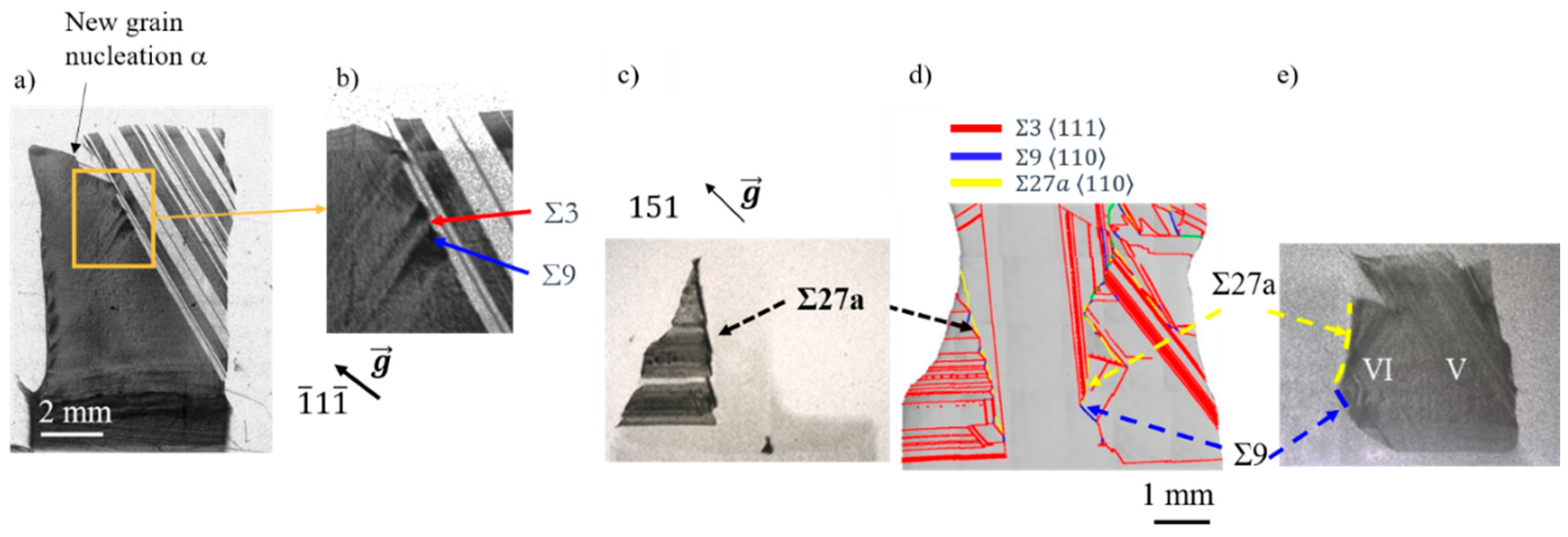
3.2.1. Twin Nucleation

Four typical final grain structures of samples solidified from a seed in the GaTSBI DS furnace are shown in Figure 6. The coincidence site lattice maps (middle line in Figure 6) are shown in order to reveal the grain boundary character and in particular the twin boundaries. These samples are solidified from float-zone (FZ) monocrystalline seeds (Figure 6a,b) and from Czochralski (Cz) seeds (Figure 6c,d) after partial melting of the seed. The samples are solidified from seeds with different crystallographic orientations in the growth direction (Figure 6 bottom line). In all cases, side twins develop at the edges from {111} facets and compete with the main central grain issued from the seed, as it was also observed by Trempa et al. [7] in a systematic study. The fact that the behavior of FZ and Cz seeds is comparable suggests that the presence of oxygen (typically: 0.5–1 × 10¹⁸ at/cm3 in Cz ingots compared to <1015 at/cm3 in FZ ingots) is not a predominant factor for the twin nucleation.
Figure 5a,b corresponds to a snapshot at one instant during solidification showing the solid–liquid interface of samples in Figure 6a,c, respectively. The in situ X-ray radiography images (Figure 5) reveals that the solid–liquid interface is smooth during growth under these conditions for both Cz (Figure 5a) and FZ (Figure 5b) seeds. No destabilization of the interface can be observed in all cases when Cz or FZ seeds are used. Interface destabilization has only been observed in the presence of Cu impurities as reported in [53].
Despite the global smooth interface, {111} facets can be clearly seen on the X-ray radiography images at the edges of the sample (Figure 5). It was verified that they correspond to the projection of {111} facets by determining the corresponding pole figures using the measurements performed by EBSD. The {111} facet orientation is highlighted by the red lines in Figure 5. Twin nucleation takes place regularly on these {111} facets as can be seen for example in Figure 5a (right) and Figure 5b (left). A video of radiograph images showing the dynamic evolution of the solid–liquid interface during the experiment corresponding to Figure 2, Figure 5a, and Figure 6a is provided as supplementary material (Video S1). It evidences twin nucleation at the {111} edge facets and the formation of grain boundary grooves at the solid–liquid interface due to the subsequent grain competition.
Diffraction spot images collected at different times during the solidification of the two samples (corresponding to the experiments and grain structure in Figure 6c,d) are shown in Figure 7. The diffraction spots in Figure 7a display the twinning zone at the right side of the sample in Figure 6d, whereas the diffraction spots in Figure 7b display the twinning zone at the left side of the sample in Figure 6c. The purple dotted line is added in Figure 7a to indicate the corresponding solid–liquid interface shape as observed in the radiographs. It is worth reminding that diffraction imaging shows only the crystalline solid areas. The observation of the upper part of the diffraction spots shows that the twin nucleation occurs at the edges of the samples at the solid–liquid-vacuum-crucible phase line as also seen in the radiographs (Figure 5 and supplementary material). A sudden increase of the solid height at the solid–liquid interface is observed at the instant of each new twin nucleation on the time-resolved radiography images. From these height differences a value of the nucleation undercooling was estimated and it ranges from 0.1 to 0.5 K for the experiment corresponding to Figure 5b, Figure 6c, and Figure 7b, which is also consistent with the results reported in Section 3.1. These measurements confirm that the undercooling measured in grain boundary grooves and at the edges are sufficient for twin nucleation on the {111} facets.
A 3D model was proposed by Jhang et al. [86] to determine the nucleation probability at the level of {111} facets. This model was specifically applied to several of our experimental cases. The nucleation probability of twin grains was found to be higher when there is a contact between the {111} facet and crucible walls. This is generally the case in our thin sample configuration. Additionally, the authors showed that the attachment energy and the contact area with crucible walls are the key factors for the heterogeneous nucleation of twins. Low attachment energy and lower contact area concur to the highest twining probability on the {111} facets. When applied to our experimental case, it is found that twin grain nucleation probability is higher at the sample edge {111} facets compared to the ones situated in grain boundary grooves, where the attachment energy and the bottom contact area of the twin nucleus tend to be lower. This is in agreement with the experimental observations.
Moreover, the twin growth rate at the nucleation instant (about 15 µm/s) exceeds the one of the global solid–liquid interface (2 µm/s). The consequence is that the twin grains that nucleate on the edges grow vertically very fast and in advance compared to the global solid–liquid interface inducing the triangular images recorded on the topographs during solidification. Such a triangular shape of the twins growing at the solid–liquid interface was repeatedly observed in our experiments. When the crystal arrives at the liquidus isotherm position, stabilization of the growth rate is observed until the global solid–liquid interface arrives at the liquidus. As a subsequent step, a growth rate plateau is measured, after which the next twin nucleation can take place [45]. The nucleation of the twin and growth upwards along the directional solidification direction goes along with the propagation of the twin grains towards the center as revealed by the topographs (Figure 7).
A main result of our work is that only Σ3 type twinned grains nucleate during growth. This conclusion can only be drawn because we are able to monitor the growth in situ with X-ray imaging.

3.2.2. Successive Twinning

The successive twinning zones are immediately identifiable on ingots after solidification. It is evidenced on both the grain structure EBSD maps (Figure 6, upper line) and diffraction images for example on Figure 2, Figure 3, and Figure 7. The successive twinning zone is observable by the alternation of two crystallographic orientations (Figure 6) on the EBSD maps and by the striped/hatched aspect of the topographs (Figure 2, Figure 3, and Figure 7). Only two crystallographic orientations alternate, and they share a common {111} plane. The fact that crystallographic orientations are found successively can be explained by the orientation of both seed and first twin grain. The stereographic projection of {111} planes of both the seed and first twin grain (green and pink color in Figure 6c, respectively) corresponding to Figure 6c and Figure 7b is shown in Figure 7c. These two stereographic projections are sufficient to describe the grains of the entire twinning zone because only two crystallographic orientations are successively repeated. The seed (Figure 7c left) presents four {111} planes, two with a vertical projection parallel to the growth direction, and two {111} planes presenting a horizontal projection perpendicular to the growth direction and facing the liquid. The first nucleus initiated at the left edge of the sample nucleates on the {111} facet having a horizontal projection (Figure 7c right). This is confirmed by the existence of a common {111} plane between the seed and the horizontal twin. Then, as a subsequent step, the first twin has only one {111} plane presenting a horizontal projection perpendicular to the growth direction and facing the liquid. The next Σ3 twin nucleating on this {111} facet has the same orientation as the initial seed so that the crystallographic orientation is alternately retrieved.

3.2.3. Twin Growth

Once a twin nucleus appears at the sample edges on a {111} facet, it grows laterally as shown by the in situ radiography and topography images. Twin grains grow towards the central part along their respective {111} facets until they meet the grain that took over from the seed or other twinned grains (Figure 6). Indeed, the progress of the pristine grain issued from the seed can be stopped by the competition with twinned grains as for example in Figure 6a,b. This is in fact totally controlled by the relative orientation of the seed that determines the orientation of the {111} facets initiating twinning as can be seen on the sketch showing the {111} facet orientations of the seeds in Figure 6 (bottom line) and as studied by Trempa et al. [7].

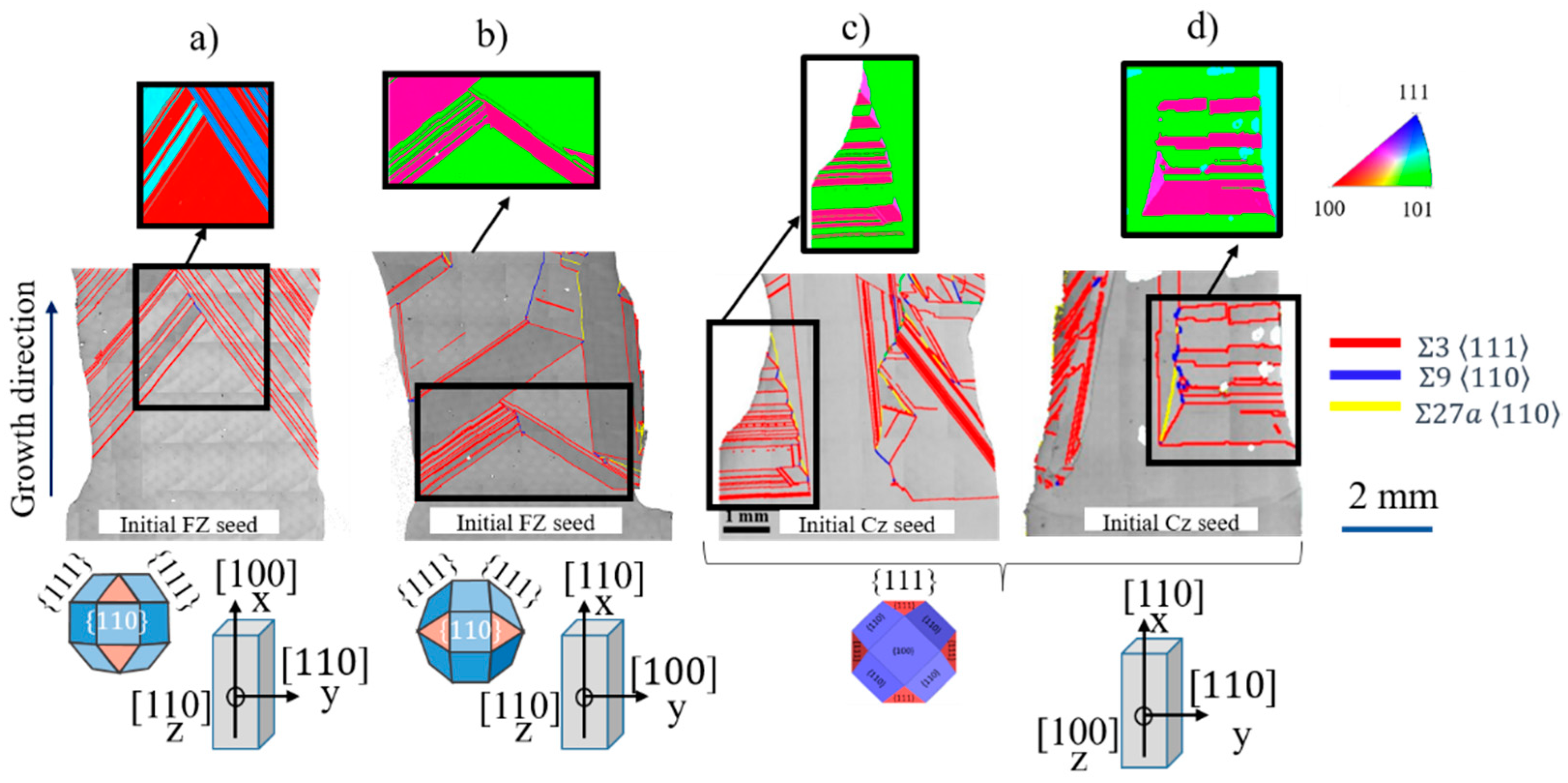
3.3. Grain Competition and Higher Order Twin Boundaries

The encounter of twinned grains with other grains creates grain boundaries, which leads to the formation of grain boundary grooves at the solid–liquid interface (see as well supplementary material). The grain boundary type formed is directly linked to the crystallographic orientation of the adjacent grains. As seen above, the Σ3 type twinned grains are the only ones to nucleate during growth, so higher order twin boundaries such as Σ9 <110> and Σ27a <110> are in all the experimental cases (FZ or Cz seeds) only the result of grain encounter and competition. A statistical analysis on the percentage of the different types of twin boundaries in relation to the total number of twin boundaries was obtained from EBSD measurements after the last solidification experiment on several samples from FZ seeding to exclude the influence of impurities. It is clearly seen that the majority of twin boundaries are of Σ3 type (typically more than 90%). Whereas the proportion of Σ3 twin boundaries is regularly retrieved for these pure seed samples, the proportion of higher order twin boundaries depends on the growth and nucleation events. As the samples grow, more Σ3 twin grains nucleate so that encounters are more likely to occur increasing the amount of higher order twin boundaries. It is worth noting that a different behavior was observed in samples containing higher levels of impurities for which although the predominance of Σ3 twin grains is still maintained, other grain nucleation events can take place [53]. The experimental results shown in Figure 2 and Figure 6a have been recently simulated using a 3D cellular automaton model of the grain structure [76]. The dynamics of {111} facets and the nucleation, growth, and competition of grains in twin relationship could be modelled and compared successfully to the experiments. The application of this model to larger scale ingot solidification is foreseen.

3.4. Strain Building During Growth

The study of local strain development during growth (deformation) is of great importance as local deformations can lead to the formation of dislocations, which are major defects affecting the material electrical properties as seen in the introduction. On the one hand, dislocations can develop during the cooling down of the sample following the solidification due to the Alexander–Haasen model [87]. On the other hand, the local nucleation of dislocation clusters is expected to take place during crystal growth [88,89].
Before presenting results on strain building, it is important to specify that during the heating segment of the experimental procedure, dislocations appear in the sample as described in [71] and remain in the seed kept after partial melting. During solidification, these dislocations develop, usually along the growth direction and can encounter grain boundaries. Dislocations can be stopped and accumulate, unless they are able to cross-slip at the level of a grain boundary which is most likely to occur at Σ3 type twin boundaries because of the presence of a {111} possible gliding plane [45]. For example, in nickel [90], coherent Σ3 twin boundaries act as effective barriers to slip except in the case of screw dislocations which can direct or cross slip across the boundary using the {111} boundary plane itself. During growth, dislocations can propagate or cross slip and propagate along the {111} planes until they reach a free surface or meet another interface.

3.4.1. Strain and Σ3{111}1,2 Twins

Strain is observed at the location of twin nucleation as can be clearly seen on the topographs in Figure 2d and Figure 3. It is revealed by the enhanced black contrast observed at the location of twin nucleation. Although the apparition of these contrasts is concomitant to twin nucleation and beginning of growth, it is not possible at present to determine if the deformation is present just before or just after the nucleation event. This is one aspect that will be studied in more details in the future. A video of topographs showing twinning and strain formation during solidification in the experiment corresponding to Figure 3 is provided as supplementary material (Video S2). As explained in Section 2, dislocations can be clearly evidenced as well as their interaction with twin boundaries. Besides, a black contrast observed at the level of twin nucleation (Figure 2) is retrieved on the projected image of the solid–liquid interface. It can be associated to the gliding of dislocations along the {111} facets that exit at the solid–liquid interface confirming that dislocations can in some cases glide along these planes as also seen in [45].

3.4.2. Strain Building Due to Competition

Local strain heterogeneities are also created due to grain competition. This is clearly evidenced in the topographs shown in Figure 8. Comparing the CSL map (Figure 6a) with the respective diffraction image (Figure 8a,b), it can be concluded that no local strain accumulation occurred at the level of Σ3 twin boundaries except at the nucleation location as discussed above. On the contrary, a localized strain field is characterized at the position of Σ9 twin boundaries as evidenced by the black contrast on the topograph (Figure 8b). This is expected as in the case of Σ9 twin boundaries, cross slip is unlikely. Only the dislocations having the Burgers vector directions of a common rotation axis <110> to build a symmetric grain boundary can cross slip; for other rotation axes, cross slip is not possible. As a consequence, dislocations and strain accumulate at the level of the Σ9 twin boundary. The same observation is made for all successive twins each time Σ3 and Σ9 twin boundaries are formed due to competition. Moreover, it is worth noting that the strain created by the grain competition seems to propagate over longer distances in the samples. This is evidenced by the expansion over a few millimeters of the black contrast from the competition zone on the right side of the sample (Figure 8b).
This observation is not a single observation corresponding to a particular experiment but was repeatedly observed during solidification. As discussed in Section 3.2, in successive twinning configuration, due to the alternated twin crystallographic orientations, the same grain boundary types are retrieved alternately. In the experiment presented in Figure 8a,b, Σ3 and Σ9 twin boundaries are formed and are observed in sequence which means that local deformations are built successively according to the grain boundary type. On the experiment shown in Figure 8c–e, Σ3 and Σ9 twin boundaries are also formed and are observed in sequence as well as Σ27a type twin boundaries. For the later grain boundary type, high strained zones (Figure 8c,d) are created which could be due to the accumulation of already present dislocations that cannot cross slip or to the emission of dislocations from these imperfect grain boundaries from the crystallographic point of view. Dislocation emission is clearly observed at the level of a Σ27a type twin boundary (Figure 8e).

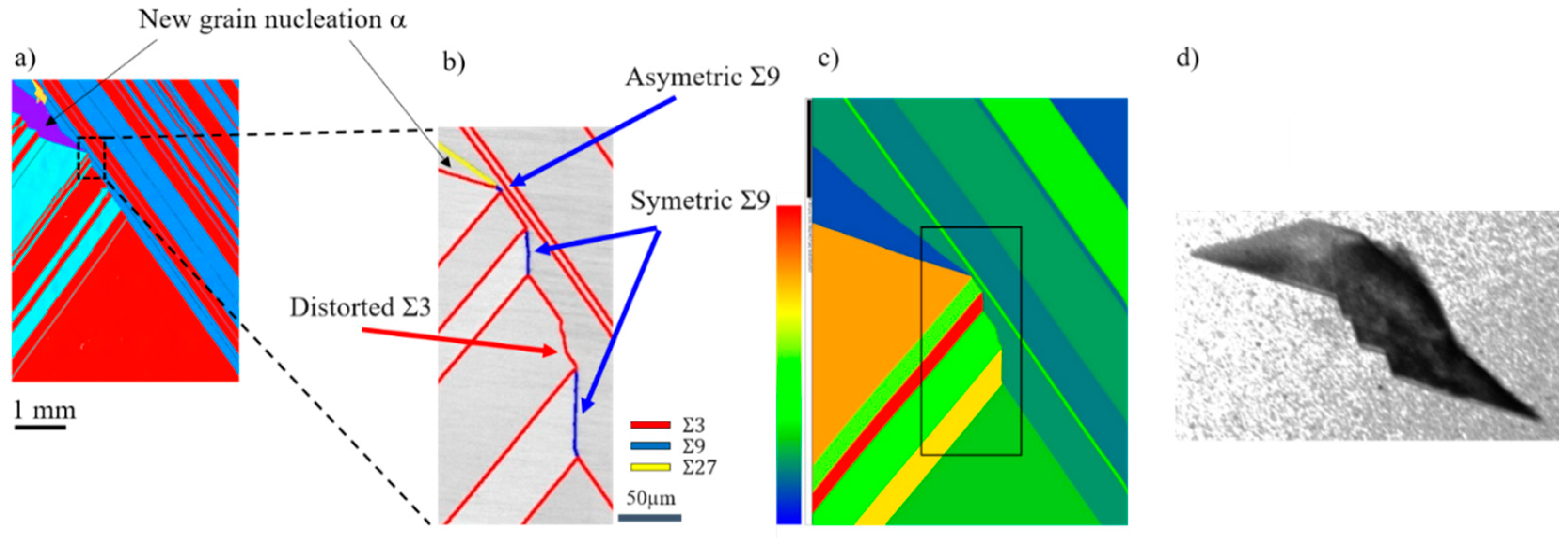
3.4.3. Grain Nucleation Related to Strain Accumulation

Strain building during growth has a high impact on the generation of dislocations but it is also associated to spontaneous new grain nucleation. In the experiment shown in Figure 8a,b, after twin nucleation, a grain boundary is regularly formed when twins coming from both sides meet. The grain boundary leads to the formation of a grain boundary groove at the solid–liquid interface. The phenomenon takes place until a new grain nucleates in the grain boundary groove. This grain nucleation event has been observed in several experiments. The nucleation of grain α (Figure 8a and Figure 9) is of particular interest. This grain has a different crystallographic orientation compared to the seed and to the twins on the right and left as evidenced by the topograph in Figure 8a and by the inverse pole figure map in Figure 9a. However, it is in fact a twinned grain that nucleated on the left {111} facet of the grain boundary groove as shown by the Σ3 twin boundary on its left-hand side (Figure 9b).
Several phenomena are at the origin of the nucleation of this particular grain at the level of the grain boundary groove. The first reason is that the undercooling inside a grain boundary groove is higher than at the level of the solid–liquid interface as discussed in Section 3.1 and in our previous work [48] which facilitates grain nucleation in this area. However, it is not a sufficient reason to explain the nucleation at this particular instant as a grain boundary groove was repeatedly formed at the encounter between twins nucleating from the left and right during the experiment. In fact, the grain competition dynamics imposes the formation of twin boundaries non-symmetric or of distorted grain boundaries and induces at the same time accumulation of crystal structure deformation both described in the following for this particular experiment.
The growth dynamic competition between twin grains coming from the left and right leads to the formation of a distorted Σ 3 twin boundary (Figure 9b) at first twin encounter. This distorted Σ3 twin boundary gradually evolves to the ideal orientation and straightness of a symmetric {111} Σ3 twin boundary during growth. Besides, due to the relative crystallographic orientations of the twin grains, Σ3 and Σ9 twin boundaries are alternately formed. Due to the competition and growth dynamics, some of the Σ9 are forced to adopt an asymmetric configuration {111}/{115} (Figure 9b). The Σ9 twin boundary asymmetric configuration corresponds to a higher grain boundary energy [91]. In fact, it was reported by TEM (transmission electron microscopy) studies coupled to DFT (density functional theory) [92] that on the contrary to the Σ9 {122}1,2 grain boundary, the atomic structure of the asymmetric Σ9 {111}/{115} one shows strong distortions. Its energy is about twice as high as that of the symmetric Σ9 {122}1,2. As a consequence, this situation is unstable from an energetic point of view and not favorable. Just before the nucleation of grain α, at the level of the encounter with a new twin grain from the right, a tiny asymmetric Σ9 {111}/{115} twin boundary is created. As seen above, non-symmetrical grain boundaries are deformed at the atomic scale [91] and offer greater resistance for dislocation crossing, thereby creating higher strain [90] and structure deformation, promoting dislocation emission. Indeed, the competition goes along with an increasing accumulation of strain when Σ9 twin boundaries are present which is also revealed by both diffraction images in situ during growth and grain orientation spread map (GOS) determined from ex situ EBSD measurements after cooling down of the sample (Figure 9c).
The nucleation in presence of strain accumulation can be triggered by energetic reasons as well as by the existence of the associated dislocations [46]. Indeed, dislocations can favor nucleation by decreasing the nucleation undercooling as discussed in Section 3.1. In Figure 9d showing a topograph corresponding to grain α, it can be seen that the highest strain level (darker contrast) is localized at the position of its nucleation and beginning of its growth. During its growth, the strain level decreases as evidenced by the lighter contrast on the top left side (Figure 9d). Inside the grain α, local strain and dislocation emission are also observed in the right upper region (Figure 9d). It is due to another phenomenon, namely, the competition between grains on the right and this newly nucleated grain that tends to extend in the solidification direction. Due to the relative crystallographic orientations of both grains, a Σ27 twin boundary is formed at this level and this type of twin boundary is prone to crystal structure deformation and associated dislocation emission as seen above and in [45,93].
Generally, the new type α grain nucleation contributes to obtain a better crystalline quality in the upper part of the ingot. A lower strain level is observed in the upper growing grains as can be seen in the GOS map (Figure 9c). Grains above this nucleation event are generally less deformed at the scale of the grain structure and more locally inside the grain that nucleated (Figure 9d). Strain redistribution cannot be invoked in our experimental case as the existing strain field built during growth remains localized. Yet, the nucleation of grain α does contribute to a lower strain level in the following growth. In summary, the nucleation can be triggered by energetic reasons discussed above, by grain competition space constraints as well as by the existence of a high density of dislocations that can favor nucleation by decreasing the nucleation undercooling value. This result can be generalized because in other samples with the same crystallographic orientation, processed under similar conditions, comparable grain structures and similar nucleation events to those of grain α are observed. It is worth noting that the nucleation of grain type α is never observed at early growth stages but later during growth when strain has accumulated.
Besides, despite the subsequent deformations that can be expected and that are observed at the scale of the sample during cooling down [46], the local strain variations created during growth and due to grain nucleation, competition, and strain building during growth are retrieved after cooling down as can be seen on the GOS map that was recorded ex situ and with rocking curve imaging in our previous work [45]. These deformed regions remain in the material. They can generate dislocations during growth and be at the origin of further dislocation emissions in subsequent steps of the solar cell fabrication process.

4. Conclusions

The combination of X-ray radiography and topography imaging achieved in situ during the solidification of Si using the GaTSBI tool has proven its efficiency to unveil crystal growth mechanisms. Time-resolved phenomena that occur during crystal growth such as grain nucleation, grain competition, twin formation, defect generation, and their evolution and interaction with grains are followed and investigated in real time.
The growth of {111} facets at grain boundary grooves and at the edges of the sample was investigated. Nucleation of twin crystals are found to occur preferentially on {111} facets at the edges of the sample where solid–liquid–vapor triple point lines exist and at the location where the sample is in contact with the crucible as well. Nucleation can also take place at the level of {111} facets in grain boundary grooves formed by a grain boundary at the solid–liquid interface. In our growth parameter range, the undercooling at the level of {111} facets at the edges and in grain boundary grooves is always lower than 1 K relatively to the solid–liquid interface, which is sufficient for twin nucleation. Since the undercooling on facets at the edges is higher than the undercooling on facets inside grain boundary grooves, there is a higher nucleation probability at the edges resulting in regular and successive twinning from the sides. Additionally, when studying the {111} facet growth laws, it appears that the experimental results can only be compared reasonably to the quadratic growth law which relies on the presence of dislocations that enhances growth which is highly probable considering other experimental results revealing the presence of dislocations during growth.
We show that twinning observed with our processing conditions is a growth rather than a deformation phenomenon. Moreover, only Σ3 twins nucleate during growth, higher order grain boundaries being solely the result of grain competition. One consequence is that the majority of the grain boundaries in the solidified ingot are of Σ3 types in samples grown from pure monocrystalline seeds at least while the competition effect is not dominant.
The competition and formation of higher order twin boundaries go along with deformations and the accumulation of dislocations. The dislocation behavior when encountering grain boundaries varies according to the types of grain boundaries. Lower or no dislocation accumulation and deformation are observed at the level of Σ3 twin boundaries. Indeed, there is a higher probability that dislocations can move along Σ3 twin boundaries due to the {111} common glide planes that exist at the level of Σ3 twin boundaries compared to the case of higher order twin boundaries. Strain is observed in all cases at the level of higher order twin boundaries either because cross-slip of dislocations is not possible and/or because they are responsible for the emission of dislocations as observed in particular for Σ27a <110> grain boundaries. Such accumulation can be at the origin of significant crystal structure deformations in the samples. Specifically, areas in which Σ27a <110> grain boundaries are present are more distorted than the average distortion of the sample. On top of that, the character of the grain boundary (coherent or incoherent) and its Σ-type, its deviation from the optimum orientation and the symmetry or non-symmetry of the boundary planes have an impact on the distortion of the formed boundary and on the emission of dislocations in the vicinity of the surrounding grains as well.
Strain building during growth has a high impact on the generation of dislocations but it is also associated with spontaneous grain nucleation. This kind of nucleation event contributes to the recovery of a lower strain level in the upper growing grains. The nucleation in presence of strain accumulation can be triggered by energetic reasons as well as by the existence of associated dislocations. Indeed, dislocations can favor nucleation by decreasing the nucleation undercooling. Another main result is that local strain at the grain scale, which is revealed and monitored during solidification, is retrieved in the ingot after cooling down even though additional strain is created during the cooling down step. However, no detectable additional twin nucleation is observed during cooling down.
The enhancement of the recording frequency now provides the opportunity to study the propagation, multiplication, and rearrangement of dislocations by interactions with themselves, grain boundaries, and the solid–liquid interface, during the whole process. This includes dislocation generation and motion in the seed crystal at high temperature up to the melting point as well as dislocation multiplication and rearrangement during melting, solidification, and cooling. In the future, further experiments will be conducted to develop and deepen the investigation of these phenomena. Our work clearly shows that local strain can be built during growth and the synchronization of X-ray radiography and Bragg diffraction imaging (topography) will allow an enhanced monitoring of strain building. The impact of impurities is not discussed in detail in the present manuscript. However, the effect of carbon, oxygen, and metallic impurities on grain nucleation and competition is being studied as this is an essential aspect for industrial processes.

Supplementary Materials

The following are available online at https://www.mdpi.com/2073-4352/10/7/555/s1. Video S1: Video of radiographs showing the dynamic evolution of the solid–liquid interface during the experiment corresponding to Figure 2, Figure 5a, and Figure 6a, Video S2: Video of topographs showing twinning and strain formation during solidification in the experiment corresponding to Figure 3.

Author Contributions

Conceptualization, N.M.-N., G.R. (Gabrielle Regula), G.R. (Guillaume Reinhart), L.B., J.B.; methodology, N.M.-N., G.R. (Gabrielle Regula), G.R. (Guillaume Reinhart); validation, N.M.-N., G.R. (Gabrielle Regula), G.R. (Guillaume Reinhart), I.P., J.B.; formal analysis, N.M.-N., G.R. (Gabrielle Regula), G.R. (Guillaume Reinhart), J.B., M.B., H.O., T.R.-B., M.T., V.S., F.G., L.B., I.P.; investigation, N.M.-N., G.R. (Gabrielle Regula), G.R. (Guillaume Reinhart), M.B., H.O., T.R.-B., M.T.; resources, J.-P.V., A.R., E.B., L.B., F.G.; data curation, N.M.-N.; writing—original draft preparation, N.M.-N.; writing—review and editing, N.M.-N.; visualization, M.B., H.O., T.R.-B., M.T., V.S., F.G.; supervision, N.M.-N.; project administration, N.M.-N.; funding acquisition, N.M.-N., M.B. All authors have read and agreed to the published version of the manuscript.

Funding

This research was funded by Agence Nationale de la Recherche (grant No. 14-CE05-0046-01, CrySaLID project) and Deutsche Forschungsgemeinschaft (scholarship No. BE 6627/1-1 to Maike Becker).

Acknowledgments

The ESRF (European Synchrotron Radiation Facility) BM05 team is acknowledged for support during some of the X-ray imaging experiments presented in this manuscript.

Conflicts of Interest

The authors declare no conflict of interest.

References

  1. Usami, N.; Takahashi, I.; Kutsukake, K.; Fujiwara, K.; Nakajima, K. Implementation of faceted dendrite growth on floating cast method to realize high-quality multicrsytalline Si ingot for solar cells. J. Appl. Phys. 2011, 109, 083527. [Google Scholar] [CrossRef]
  2. Fujiwara, K.; Pan, W.; Usami, N.; Sawada, K.; Tokairin, M.; Nose, Y.; Nomura, A.; Shishido, T.; Nakajima, K. Growth of structure-controlled polycrystalline silicon ingots for solar cells by casting. Acta Mater. 2006, 54, 3191–3197. [Google Scholar] [CrossRef]
  3. Jouini, A.; Ponthenier, D.; Lignier, H.; Enjalbert, N.; Marie, B.; Drevet, B.; Pihan, E.; Cayron, C.; Lafford, T.; Camel, D. Improved multicrystalline silicon ingot crystal quality through seed growth for high efficiency solar cells. Prog. Photovolt. Res. Appl. 2012, 20, 735–746. [Google Scholar] [CrossRef]
  4. Oliveira, V.A.; Marie, B.; Cayron, C.; Marinova, M.; Tsoutsouva, M.G.; Sio, H.C.; Lafford, T.A.; Baruchel, J.; Audoit, G.; Grenier, A.; et al. Formation mechanism and properties of twinned structures in (111) seeded directionally solidified solar grade silicon. Acta Mater. 2016, 121, 24–36. [Google Scholar] [CrossRef]
  5. Stoddard, N.; Wu, B.; Witting, I.; Wagener, M.C.; Park, Y.; Rozgonyi, G.A.; Clark, R. Casting single crystal silicon: Novel defect profiles from BP solar’s mono2 TM wafers. Solid State Phenom. 2008, 131, 1–8. [Google Scholar]
  6. Lan, C.W.; Lan, A.; Yang, C.F.; Hsu, H.P.; Yang, M.; Yu, A.; Hsu, B.; Hsu, W.C.; Yang, A. The emergence of high-performance multi-crystalline silicon in photovoltaics. J. Cryst. Growth 2017, 468, 17–23. [Google Scholar] [CrossRef]
  7. Trempa, M.; Reimann, C.; Friedrich, J.; Müller, G.; Oriwol, D. Mono-crystalline growth in directional solidification of silicon with different orientation and splitting of seed crystals. J. Cryst. Growth 2012, 351, 131–140. [Google Scholar] [CrossRef]
  8. Oliveira, V.A.; Rocha, M.; Lantreibecq, A.; Tsoutsouva, M.G.; Tran-Thi, T.N.; Baruchel, J.; Camel, D. Cellular dislocations patterns in monolike silicon: Influence of stress, time under stress and impurity doping. J. Cryst. Growth 2018, 489, 42–50. [Google Scholar] [CrossRef]
  9. Tsoutsouva, M.G.; Oliveira, V.A.; Camel, D.; Baruchel, J.; Marie, B.; Lafford, T.A. Mono-like silicon ingots grown on low angle misoriented seeds: Defect characterization by synchrotron X-ray diffraction imaging. Acta Mater. 2015, 88, 112–120. [Google Scholar] [CrossRef]
  10. Tsoutsouva, M.G.; Oliveira, V.A.; Camel, D.; Tran Thi, T.N.; Baruchel, J.; Marie, B.; Lafford, T.A. Segregation, precipitation and dislocation generation between seeds in directionally solidified mono-like silicon for photovoltaic applications. J. Cryst. Growth 2014, 401, 397–403. [Google Scholar] [CrossRef]
  11. Ekstrøm, K.E.; Stokkan, G.; Søndenå, R.; Dalaker, H.; Lehmann, T.; Arnberg, L.; Di Sabatino, M. Structure and dislocation development in mono-like silicon. Phys. Status Solidi A 2015, 212, 2278–2288. [Google Scholar] [CrossRef]
  12. Autruffe, A.; Stenhjem Hagen, V.; Arnberg, L.; Di Sabatino, M. Dislocation generation at near-coincidence site lattice grain boundaries during silicon directional solidification. J. Cryst. Growth 2015, 411, 12–18. [Google Scholar] [CrossRef]
  13. Autruffe, A.; Vines, L.; Arnberg, L.; Di Sabatino, M. Coincident site lattice bi-crystals growth—Impurity segregation towards grain boundaries. J. Cryst. Growth 2015, 416, 8–11. [Google Scholar] [CrossRef]
  14. Trempa, M.; Reimann, C.; Friedrich, J.; Müller, G.; Sylla, L.; Krause, A.; Richter, T. Investigation of iron contamination of seed crystals and its impact on lifetime distribution in Quasimono silicon ingots. J. Cryst. Growth 2015, 429, 56–62. [Google Scholar] [CrossRef]
  15. Trempa, M.; Reimann, C.; Friedrich, J.; Müller, G.; Krause, A.; Sylla, L.; Richter, T. Influence of grain boundaries intentionally induced between seed plates on the defect generation in quasi-mono-crystalline silicon ingots. Cryst. Res. Technol. 2015, 50, 124–132. [Google Scholar] [CrossRef]
  16. Trempa, M.; Reimann, C.; Friedrich, J.; Müller, G.; Krause, A.; Sylla, L.; Richter, T. Defect formation induced by seed-joints during directional solidification of quasi-mono-crystalline silicon ingots. J. Cryst. Growth 2014, 405, 131–141. [Google Scholar] [CrossRef]
  17. Stokkan, G.; Song, A.; Ryningen, B. Investigation of the grain boundary character and dislocation density of different types of high performance multicrystalline silicon. Crystals 2018, 8, 341. [Google Scholar] [CrossRef] [Green Version]
  18. Hurle, D.T.J. A mechanism for twin formation during Czochralski and encapsulated vertical Bridgman growth of III–V compound semiconductors. J. Cryst. Growth 1995, 147, 239–250. [Google Scholar] [CrossRef]
  19. Von Ammon, W. FZ and CZ crystal growth: Cost driving factors and new perspectives. Phys. Status Solidi A 2014, 211, 2461–2470. [Google Scholar] [CrossRef]
  20. Oliveira, V.A.; Sio, H.C.; Faujour, A.; Piot, L.; Chabli, A.; Camel, D. Recombination activity of 2D extended defects in monolike silicon. Energy Procedia 2016, 92, 755–763. [Google Scholar] [CrossRef] [Green Version]
  21. Woo, S.; Bertoni, M.; Choi, K.; Nam, S.; Castellanos, S.; Powell, D.M.; Buonassisi, T.; Choi, H. An insight into dislocation density reduction in multicrystalline silicon. Sol. Energy Mater. Sol. Cells 2016, 155, 88–100. [Google Scholar] [CrossRef]
  22. Wang, Z.-J.; Tsurekawa, S.; Ikeda, K.; Sekiguchi, T.; Watanabe, T. Relationship between electrical activity and grain boundary structural configuration in polycrystalline silicon. Interface Sci. 1999, 7, 197–205. [Google Scholar] [CrossRef]
  23. Fedotov, A.; Evtodyi, B.; Fionova, L.; Ilyashuk, Y.; Katz, E.; Polyak, L. Electrical-activity of grain-boundaries in shaped grown silicon. Phys. Status Solidi A 1990, 119, 523–534. [Google Scholar] [CrossRef]
  24. Kivambe, M.; Ervik, T.; Ryningen, B.; Stokkan, G. On the role of stacking faults on dislocation generation and dislocation cluster formation in multicrystalline silicon. J. Appl. Phys. 2012, 112, 103528. [Google Scholar] [CrossRef]
  25. Binetti, S.; Libal, J.; Acciarri, M.; Di Sabatino, M.; Nordmark, H.; Øvrelid, E.J.; Walmsley, J.C.; Holmestad, R. Study of defects and impurities in multicrystalline silicon grown from metallurgical silicon feedstock. Mater. Sci. Eng. B 2009, 159, 274–277. [Google Scholar] [CrossRef]
  26. Oriwol, D.; Carl, E.R.; Danilewsky, A.N.; Sylla, L.; Seifert, W.; Kittler, M.; Leipner, H.S. Small-angle subgrain boundaries emanating from dislocation pile-ups in multicrystalline silicon studied with synchrotron white-beam X-ray topography. Acta Mater. 2013, 61, 6903–6910. [Google Scholar] [CrossRef]
  27. Adamczyk, K.; Søndenå, R.; Stokkan, G.; Looney, E.; Jensen, M.; Lai, B.; Rinio, M.; Sabatino, M.D. Recombination activity of grain boundaries in high-performance multicrystalline Si during solar cell processing. J. Appl. Phys. 2018, 123, 055705. [Google Scholar] [CrossRef]
  28. Wang, H.Y.; Usami, N.; Fujiwara, K.; Kutsukake, K.; Nakajima, K. Microstructures of Si multicrystals and their impact on minority carrier diffusion length. Acta Mater. 2009, 57, 3268–3276. [Google Scholar] [CrossRef]
  29. Autruffe, A.; Søndenå, R.; Vines, L.; Arnberg, L.; Di Sabatino, M. Influence of pulling rate on multicrystalline silicon ingots’ properties. J. Cryst. Growth 2014, 386, 199–203. [Google Scholar] [CrossRef]
  30. Duffar, T. Comprehensive review on grain and twin structures in bulk photovoltaic silicon. Recent Res. Dev. Cryst. Growth 2009, 5, 61–111. [Google Scholar]
  31. Gallien, B.; Duffar, T.; Lay, S.; Robaut, F. Analysis of grain orientationin cold crucible continuous casting of photovoltaic Si. J. Cryst. Growth 2011, 318, 208–211. [Google Scholar] [CrossRef]
  32. Lan, C.W.; Lee, T.F.; Yu, A.; Yang, Y.M.; Hsu, W.C.; Hsu, B.; Yang, A. Grain control in directional solidification of photovoltaic silicon. J. Cryst. Growth 2012, 360, 68–75. [Google Scholar] [CrossRef]
  33. Reimann, C.; Müller, G.; Friedrich, J.; Lauer, K.; Simonis, A.; Wätzig, H.; Krehan, S.; Hartmann, R.; Kruse, A. Systematic characterization of multi-crystalline silicon String Ribbon wafer. J. Cryst. Growth 2012, 361, 38–43. [Google Scholar] [CrossRef]
  34. Zhou, N.; Wei, X.; Zhou, L. Formation of dislocations in the growth of silicon along different crystallographic directions—A molecular dynamics study. Crystals 2018, 8, 346. [Google Scholar] [CrossRef] [Green Version]
  35. Nagashio, K.; Adachi, M.; Higuchi, K.; Mizuno, A.; Watanabe, M.; Kuribayashi, K.; Katayama, Y. Real-time x-ray observation of solidification from undercooled Si melt. J. Appl. Phys. 2006, 100, 033524. [Google Scholar] [CrossRef]
  36. Nagashio, K.; Murata, H.; Kuribayashi, K. In situ observation of solidification behavior of Si melt dropped on Si wafer by IR thermography. J. Cryst. Growth 2005, 275, e1685–e1690. [Google Scholar] [CrossRef]
  37. Fujiwara, K.; Maeda, K.; Usami, N.; Sazaki, G.; Nose, Y.; Nomura, A.; Shishido, T.; Nakajima, K. In situ observation of Si faceted dendrite growth from low-degree-of-undercooling melts. Acta Mater. 2008, 56, 2663–2668. [Google Scholar] [CrossRef]
  38. Fujiwara, K.; Obinata, Y.; Ujihara, T.; Usami, N.; Sazaki, G.; Nakajima, K. Grain growth behaviors of polycrystalline silicon during melt growth processes. J. Cryst. Growth 2004, 266, 441–448. [Google Scholar] [CrossRef]
  39. Fujiwara, K.; Maeda, K.; Usami, N.; Sazaki, G.; Nose, Y.; Nakajima, K. Formation mechanism of parallel twins related to Si-facetted dendrite growth. Scr. Mater. 2007, 57, 81–84. [Google Scholar] [CrossRef]
  40. Fujiwara, K.; Nakajima, K.; Ujihara, T.; Usami, N.; Sazaki, G.; Hasegawa, H.; Mizoguchi, S.; Nakajima, K. In situ observations of crystal growth behavior of silicon melt. J. Cryst. Growth 2002, 243, 275–282. [Google Scholar] [CrossRef]
  41. Chuang, L.-C.; Maeda, K.; Morito, H.; Shiga, K.; Miller, W.; Fujiwara, K. In situ observation of interaction between grain boundaries during directional solidification of Si. Scr. Mater. 2018, 148, 37–41. [Google Scholar] [CrossRef]
  42. Chikawa, J.-I. Technique for the video display of X-ray topographic images and its application to the study of crystal growth. J. Cryst. Growth 1974, 24, 61–68. [Google Scholar] [CrossRef]
  43. Chikawa, J.-I.; Shirai, S. Melting of silicon crystals and a possible origin of swirl defects. J. Cryst. Growth 1977, 39, 328–340. [Google Scholar] [CrossRef]
  44. Riberi-Béridot, T.; Mangelinck-Noël, N.; Tandjaoui, A.; Reinhart, G.; Billia, B.; Lafford, T.; Baruchel, J.; Barrallier, L. On the impact of twinning on the formation of the grain structure of multi-crystalline silicon for photovoltaic applications during directional solidification. J. Cryst. Growth 2015, 418, 38–44. [Google Scholar] [CrossRef]
  45. Tsoutsouva, M.G.; Riberi-Béridot, T.; Regula, G.; Reinhart, G.; Baruchel, J.; Guittonneau, F.; Barrallier, L.; Mangelinck-Noël, N. In situ investigation of the structural defect generation and evolution during the directional solidification of <110> seeded growth Si. Acta Mater. 2016, 115, 210–223. [Google Scholar] [CrossRef]
  46. Riberi-Béridot, T.; Tsoutsouva, M.G.; Regula, G.; Reinhart, G.; Guittonneau, F.; Barrallier, L.; Mangelinck-Noël, N. Strain building and correlation with grain nucleation during silicon growth. Acta Mater. 2019, 177, 141–150. [Google Scholar] [CrossRef]
  47. Riberi-Béridot, T.; Tsoutsouva, M.G.; Regula, G.; Reinhart, G.; Périchaud, I.; Baruchel, J.; Mangelinck-Noël, N. Growth undercooling in multi-crystalline pure silicon and in silicon containing light impurities (C and O). J. Cryst. Growth 2017, 466, 64–70. [Google Scholar] [CrossRef] [Green Version]
  48. Stamelou, V.; Tsoutsouva, M.G.; Riberi-Béridot, T.; Reinhart, G.; Regula, G.; Baruchel, J.; Mangelinck-Noël, N. {111} facet growth laws and grain competition during silicon crystallization. J. Cryst. Growth 2017, 479, 1–8. [Google Scholar] [CrossRef] [Green Version]
  49. Tandjaoui, A.; Mangelinck-Noël, N.; Reinhart, G.; Billia, B.; Furter, J.J.; Lafford, T.; Baruchel, J.; Guichard, X. Real time observation of the directional solidification of multicrystalline silicon: X-ray imaging characterization. Energy Procedia 2012, 27, 82–87. [Google Scholar] [CrossRef] [Green Version]
  50. Tandjaoui, A.; Mangelinck-Noël, N.; Reinhart, G.; Billia, B.; Guichard, X. Twinning occurrence and grain competition in multicrystalline silicon during solidification. C. R. Phys. 2013, 14, 8. [Google Scholar] [CrossRef]
  51. Tandjaoui, A.; Mangelinck-Noel, N.; Reinhart, G.; Billia, B.; Lafford, T.; Baruchel, J. Investigation of grain boundary grooves at the solid–liquid interface during directional solidification of multi-crystalline silicon: In situ characterization by X-ray imaging. J. Cryst. Growth 2013, 377, 203–211. [Google Scholar] [CrossRef]
  52. Becker, M.; Regula, G.; Reinhart, G.; Boller, E.; Valade, J.-P.; Rack, A.; Tafforeau, P.; Mangelinck-Noel, N. Simultaneous X-ray radiography and diffraction topography imaging applied to silicon for defect analysis during melting and crystallization. J. Appl. Crystallogr. 2019, 52, 1312–1320. [Google Scholar] [CrossRef]
  53. Ouaddah, H.; Périchaud, I.; Barakel, D.; Palais, O.; Di Sabatino, M.; Reinhart, G.; Regula, G.; Mangelinck-Noël, N. Role of impurities in silicon solidification and electrical properties studied by complementary In Situ and Ex Situ methods. Phys. Status Solidi A 2019, 216, 1–10. [Google Scholar] [CrossRef] [Green Version]
  54. Baruchel, J.; Buffiere, J.-Y.; Cloetens, P.; Di Michiel, M.; Ferrie, E.; Ludwig, W.; Maire, E.; Salvo, L. Advances in synchrotron radiation microtomography. Scr. Mater. 2006, 55, 41–46. [Google Scholar] [CrossRef]
  55. Cloetens, P.; Barrett, R.; Baruchel, J.; Guigay, J.-P.; Schlenker, M. Phase objects in synchrotron radiation hard x-ray imaging. J. Phys. D Appl. Phys. 1996, 29, 133–146. [Google Scholar] [CrossRef]
  56. Reinhart, G.; Grange, D.; Abou-Khalil, L.; Mangelinck-Noël, N.; Niane, N.T.; Maguin, V.; Guillemot, G.; Gandin, C.A.; Nguyen-Thi, H. Impact of solute flow during directional solidification of a Ni-based alloy: In-situ and real-time X-radiography. Acta Mater. 2020, 194, 68–79. [Google Scholar] [CrossRef]
  57. Schneider, C.A.; Rasband, W.S.; Eliceiri, K.W. NIH Image to ImageJ: 25 years of image analysis. Nat. Methods 2012, 9, 671–675. [Google Scholar] [CrossRef]
  58. Mittone, A.; Manakov, I.; Broche, L.; Jarnias, C.; Coan, P.; Bravin, A. Characterization of a sCMOS-based high-resolution imaging system. J. Synchrotron Radiat. 2017, 24, 1226–1236. [Google Scholar] [CrossRef]
  59. Lang, A.R. The early days of high-resolution X-ray topography. J. Phys. D Appl. Phys. 1993, 26, A1–A8. [Google Scholar] [CrossRef]
  60. Härtwig, J. Hierarchy of dynamical theories of x-ray diffraction for deformed and perfect crystals. J. Phys. D Appl. Phys. 2001, 34, A70–A77. [Google Scholar] [CrossRef]
  61. Burns, R.C.; Chumakov, A.I.; Connell, S.H.; Dube, D.; Godfried, H.P.; Hansen, J.O.; Härtwig, J.; Hoszowska, J.; Masiello, F.; Mkhonza, L.; et al. HPHT growth and x-ray characterization of high-quality type IIa diamond. J. Phys. Condens. Matter 2009, 21, 364224. [Google Scholar] [CrossRef] [PubMed]
  62. Authier, A. Contrast of dislocation images in X-Ray transmission topography. Adv. X Ray Anal. 1966, 10, 9–31. [Google Scholar] [CrossRef]
  63. De Graef, M.; McHenry, M.E. Structure of Materials: An Introduction to Crystallography, Diffraction and Symmetry; Cambridge University Press: Cambridge, UK, 2007. [Google Scholar]
  64. Danilewsky, A.N.; Wittge, J.; Croell, A.; Allen, D.; McNally, P.; Vagovič, P.; Dos Santos Rolo, T.; Li, Z.; Baumbach, T.; Gorostegui-Colinas, E.; et al. Dislocation dynamics and slip band formation in silicon: In-situ study by X-ray diffraction imaging. J. Cryst. Growth 2011, 318, 1157–1163. [Google Scholar] [CrossRef]
  65. Vallino, F.; Chateau, J.P.; Jacques, A.; George, A. Dislocation multiplication during the very first stages of plastic deformation in silicon observed by X-ray topography. Mat. Sci. Eng. A 2001, 319, 152–155. [Google Scholar] [CrossRef]
  66. Danilewsky, A.; Wittge, J.; Kiefl, K.; Allen, D.; McNally, P.; Garagorri, J.; Elizalde, M.R.; Baumbach, T.; Tanner, B.K. Crack propagation and fracture in silicon wafers under thermal stress. J. Appl. Crystallogr. 2013, 46 Pt 4, 849–855. [Google Scholar] [CrossRef] [Green Version]
  67. Lafford, T.A.; Villanova, J.; Plassat, N.; Dubois, S.; Camel, D. Synchrotron X-ray imaging applied to solar photovoltaic silicon. J. Phys. Conf. Ser. 2013, 425, 192019. [Google Scholar] [CrossRef] [Green Version]
  68. Yao, Y.; Sugawara, Y.; Ishikawa, Y. Observation of dislocations in β-Ga2O3 single-crystal substrates by synchrotron X-ray topography, chemical etching, and transmission electron microscopy. Jpn. J. Appl. Phys. 2020, 59, 045502. [Google Scholar] [CrossRef]
  69. Lantreibecq, A.; Monchoux, J.P.; Pihan, E.; Marie, B.; Legros, M. Subgrains, micro-twins and dislocations characterization in monolike Si using TEM and in-situ TEM. Mater. Today Proc. 2018, 5, 14732–14747. [Google Scholar] [CrossRef]
  70. Qiang, Z.; Peizhen, D.; Fuxi, G. X-ray topographic observation of dislocation structure in sapphire single crystal grown by temperature gradient technique. J. Cryst. Growth 1991, 108, 377–384. [Google Scholar] [CrossRef]
  71. Tsoutsouva, M.G.; Riberi-Béridot, T.; Regula, G.; Reinhart, G.; Baruchel, J.; Mangelinck-Noël, N. In Situ imaging of dislocation expansion in FZ-Si seeds during temperature ramp heating process. Phys. Status Solidi A 2018, 215, 1700758. [Google Scholar] [CrossRef]
  72. Miller, W. Some remarks on the undercooling of the Si(111) facet and the “Monte Carlo modeling of silicon crystal growth” by Kirk M. Beatty & Kenneth A.; Jackson, J. Crystal Growth 211 (2000) 13. J. Cryst. Growth 2011, 325, 101–103. [Google Scholar]
  73. Voronkov, V.V. Supercooling at the facet developing on a a rounded crystalization front. Sov. Phys. Crystallogr. 1973, 17, 807–813. [Google Scholar]
  74. Nadri, A.; Duterrail-Couvat, Y.; Duffar, T. Two-dimensional numerical modeling of grain structure in multi-crystalline silicon ingot. J. Cryst. Growth 2014, 385, 16–21. [Google Scholar] [CrossRef]
  75. Lin, H.K.; Lan, C.W. Phase field modeling of grain structure evolution during directional solidification of multi-crystalline silicon sheet. J. Cryst. Growth 2017, 475, 150–157. [Google Scholar] [CrossRef]
  76. Pineau, A.; Guillemot, G.; Reinhart, G.; Regula, G.; Mangelinck-Noël, N.; Gandin, C.A. Three-dimensional cellular automaton modeling of silicon crystallization with grains in twin relationships. Acta Mater. 2020, 191, 230–244. [Google Scholar] [CrossRef]
  77. Coriell, S.R.; Sekerya, R.F. Morphological stability near a grain boundary groove in a solid-liquid interface during solidification of a binary alloy. J. Cryst. Growth 1973, 19, 285–293. [Google Scholar] [CrossRef]
  78. Duffar, T.; Nadri, A. The grain–grain–liquid triple phase line during solidification of multi-crystalline silicon. C. R. Phys. 2013, 14, 185–191. [Google Scholar] [CrossRef]
  79. Jackson, K.A. Crystal growth kinetics. Mater. Sci. Eng. 1984, 65, 7–13. [Google Scholar] [CrossRef]
  80. Dash, J.G.; Hodgkin, V.A.; Wettlaufer, J.S. Dynamics of faceted grain boundary grooves. J. Stat. Phys. 1999, 95, 1311–1322. [Google Scholar] [CrossRef]
  81. Ervik, T.; Stokkan, G.; Buonassisi, T.; Mjøs, Ø.; Lohne, O. Dislocation formation in seeds for quasi-monocrystalline silicon for solar cells. Acta Mater. 2014, 67, 199–206. [Google Scholar] [CrossRef]
  82. Lin, H.K.; Wu, M.C.; Chen, C.C.; Lan, C.W. Evolution of grain structures during directional solidification of silicon wafers. J. Cryst. Growth 2016, 439, 40–46. [Google Scholar] [CrossRef]
  83. Stockmeier, L.; Müller, G.; Seidl, A.; Lehmann, T.; Reimann, C.; Friedrich, J. Preferred grain orientations in silicon ribbons grown by the string ribbon and the edge-defined film-fed growth methods. J. Cryst. Growth 2014, 395, 74–79. [Google Scholar] [CrossRef]
  84. Heilbronn, B.; De Moro, F.; Jolivet, E.; Tupin, E.; Chau, B.; Varrot, R.; Drevet, B.; Bailly, S.; Rey, D.; Lignier, H.; et al. Fast growth of thin multi-crystalline silicon ribbons by the RST method. Cryst. Res. Technol. 2014, 50, 101–114. [Google Scholar] [CrossRef]
  85. Mangelinck-Noël, N.; Pihan, E. Le renouveau du silicium dope les pannneaux solaires. Rech. Sept. 2018, 2018, 539. [Google Scholar]
  86. Jhang, J.W.; Regula, G.; Reinhart, G.; Mangelinck-Noël, N.; Lan, C.W. Heterogeneous twinning during directional solidification of multi-crystalline silicon. J. Cryst. Growth 2019, 508, 42–49. [Google Scholar] [CrossRef] [Green Version]
  87. Alexander, H.; Haasen, P. Dislocations and plastic flow in the diamond structure. Solid State Phys. 1968, 22, 27. [Google Scholar]
  88. Takahashi, I.; Usami, N.; Kutsukake, K.; Stokkan, G.; Morishita, K.; Nakajima, K. Generation mechanism of dislocations during directional solidification of multicrystalline silicon using artificially designed seed. J. Cryst. Growth 2010, 312, 897–901. [Google Scholar] [CrossRef]
  89. Ryningen, B.; Stokkan, G.; Kivambe, M.; Ervik, T.; Lohne, O. Growth of dislocation clusters during directional solidification of multicrystalline silicon ingots. Acta Mater. 2011, 59, 7703–7710. [Google Scholar] [CrossRef]
  90. Lim, R.C.; Raj, R. Interaction between lattice and grain boundary dislocations and their role in mechanical properties of interfaces. J. Phys. Colloq. 1985, 46, 581–595. [Google Scholar] [CrossRef]
  91. Brokman, A.; Bristowe, P.D.; Balluffi, R.W. Atomistic faceting of asymmetric tilt boundaries. Scr. Metall. 1981, 15, 201–206. [Google Scholar] [CrossRef]
  92. Stoffers, A.; Ziebarth, B.; Barthel, J.; Cojocaru-Mirédin, O.; Elsässer, C.; Raabe, D. Complex nanotwin substructure of an asymmetric S9 tilt grain boundary in a silicon polycrystal. Phys. Rev. Lett. 2015, 115, 235502. [Google Scholar] [CrossRef] [PubMed] [Green Version]
  93. Stokkan, G.; Hu, Y.; Mjøs, Ø.; Juel, M. Study of evolution of dislocation clusters in high performance multicrystalline silicon. Sol. Energy Mater. Sol. Cells 2014, 130, 679–685. [Google Scholar] [CrossRef]
Figure 1. X-ray radiography image recorded during solidification (applied temperature gradient: 30 K/cm and cooling rate of −1 K/min applied on both heaters) from a FZ-Si seed. (a) Image resulting from the pixel by pixel division of the current image by the first image after starting the cooling down (α: seed–regrown interface, β: fully solid region, γ: solid–liquid interface region, δ: fully liquid region). (b) Sketch of the side view. (c) Image resulting from the pixel by pixel division of two successive raw images with a time interval of 3 s and close-up at the level of the interface at the same instant and position as in (a).
Crystals 10 00555 g001
Figure 2. X-ray diffraction images (topographs) recorded during solidification (applied temperature gradient: 30 K/cm and cooling rate of −1 K/min applied on both heaters at t0) from a FZ seed. (a) Crystallographic orientation of the seed. (b) Laue pattern recorded at the end of solidification showing the diffraction spots in the field of view. Images of the (c) 1 ¯ 1 1 ¯ and (d) 2 ¯ 20 topographs recorded at two instants during solidification.
Crystals 10 00555 g002
Figure 3. X-ray diffraction imaging (topography) during solidification (applied temperature gradient: 30 K/cm and cooling rate of −1 K/min applied on both heaters) from a FZ seed. (a) Crystallographic orientation of the seed. (b) Laue pattern showing the diffraction spots recorded at the end of solidification in the field of view. (c) Topograph of the 1 1 ¯ 1 diffraction spot during solidification.
Crystals 10 00555 g003
Figure 4. X-ray radiography images recorded during solidification, applied temperature gradient: 30 K/cm and cooling rate = −1 K/min applied on both heaters. Typical facetted/facetted grain boundary groove revealed by division by successive images.
Crystals 10 00555 g004
Figure 5. X-ray radiography images of the solid–liquid interface during growth with {111} facets at both edges of the sample for the experiments: (a) same experiment as in Figure 2 and Figure 6a, (b) same experiment as in Figure 6c. Red lines indicate the traces of {111} planes.
Crystals 10 00555 g005
Figure 6. Ex situ electron backscatter diffraction (EBSD) measurements revealing the grain structure and twin boundaries after growth and cooling down in samples grown from monocrystalline seeds. Applied temperature gradient: 30 K/cm and cooling rate applied on both heaters (a) −1 K/min (same experiment as in Figure 2, Figure 8a,b, and Figure 9), (b) −1 K/min, (c) −0.2 K/min (same experiment as in Figure 7b and Figure 8c–e), (d) applied temperature gradient: 20 K/cm and cooling rate: −0.2 K/min (same experiment as in Figure 7a). Top: Inverse Pole Figure (IPF) map along the growth direction. Middle: CSL (Coincidence Site Lattice) map. Bottom: Seed orientation and {111} planes.
Crystals 10 00555 g006
Figure 7. Image sequence of diffraction spot images—topographs corresponding to twinning zones. (a) twinning zone corresponding to the right side of sample Figure 5d. The purple dotted line corresponds to the solid–liquid interface. (b) Twinning zone corresponding to the left side of sample Figure 5c and Figure 6b. (c) Stereographic projections of the { 111 } planes of the seed (left) and the first twin (right) with both horizontal projections for the experiment in (b) and the corresponding 3D representation of the plane arrangements (below).
Crystals 10 00555 g007
Figure 8. (a) Topograph for the experiment in Figure 2, Figure 5a, and Figure 6a. (b) Close up at the level of competing twin grains, (c) topograph for the experiment in Figure 5b, Figure 6c, and Figure 7b,c, (d) corresponding coincidence site lattice map, and (e) topograph of a grain on the right side.
Crystals 10 00555 g008
Figure 9. (a) Inverse Pole Figure (IPF) map along the growth direction (same experiment as in Figure 2, Figure 5a, Figure 6a, and Figure 8a,b). (b) High resolution CSL map of the region where competition between twins take place. (c) Grain orientation spread (GOS) map of the region of the new nucleated grain (α). (d) Topograph of the grain (α).
Crystals 10 00555 g009

