Article

Research on Performance Improvement of Photovoltaic Cells and Modules Based on Black Silicon

1
School of Physics and Optoelectronic Engineering, Xidian University, Xi’an 710071, China
2
Energy Engineering School, Tianjin Sino-German University of Applied Sciences, Tianjin 300350, China
3
Tianjin Yingli New Energy Co., Ltd., Tianjin 301510, China
4
Basic Experimental Training Center, Tianjin Sino-German University of Applied Sciences, Tianjin 300350, China
*
Author to whom correspondence should be addressed.
Crystals 2020, 10(9), 753; https://doi.org/10.3390/cryst10090753
Submission received: 30 July 2020 / Revised: 21 August 2020 / Accepted: 25 August 2020 / Published: 26 August 2020
(This article belongs to the Special Issue Growth and Evaluation of Crystalline Silicon (Volume II))

Abstract

:
This paper mainly studied the electrical performance improvement of black silicon photovoltaic (PV) cells and modules. The electrical performance of the cells and modules matched with black silicon was optimized through three different experiments. Firstly, in the pre-cleaning step, the effect of lotion selection on the cell performance was studied. Compared with alkaline lotion, using acidic lotion on black silicon wafer can achieve an efficiency improvement of the black silicon cell by nearly 0.154%. Secondly, the influence of oxygen flux control of the thermal oxidation step on the improvement of cell efficiency was studied. The addition of the thermal oxidation step and its oxygen flux control resulted in an efficiency increase of the black silicon cell of nearly 0.11%. The most optimized volume control of the oxygen flux is at 2200 standard cubic centimeter per minute (SCCM). Finally, in the module packaging process, the selection of components will also greatly affect the performance of the black silicon PV module. The most reasonable selection of components can increase the output power of the black silicon PV module by 6.13 W. In a word, the technical indication of the electrical performance improvement suggested in this study plays an important guiding role in the actual production process.

Graphical Abstract

1. Introduction

With the crisis of the global fossil fuel shortage, climate warming and ecological environment deterioration are becoming more and more serious. In order to guarantee national energy security and sustainable development, more and more countries are focusing on the development and application of solar energy resources. Solar energy, as a renewable energy, is a kind of green energy with endless reserves and a wide distribution. Meanwhile, it is also clean, safe, convenient, and efficient. So, it has been considered as the best alternative to energy and has attracted wide attention around the world. Among the various ways to realize the high-efficiency utilization of solar energy, PV power generation is one of the main solar energy utilization ways, which can directly produce the electric energy that human beings depend on for survival.
As the core part of PV power generation, the electrical performance, such as maximum power and conversion efficiency (Eff), was always taken as the key indicators to measure the technical level of PV cells and modules. In the past 70 years, the innovation in materials, structure, technology, and other aspects has greatly improved the performance of crystalline silicon (c-Si) PV cells and realized industrialization. Due to the better performance than other types of PV cells, such as thin-film cells, c-Si cells have occupied the mainstream market. In 1954, the first c-Si solar cell with a P-N junction structure was made by D.M. Chapin et al. [1] in Bell Laboratory. The measured efficiency of the c-Si cell is 6%. Furthermore, the partial absorption of silicon in the solar spectrum was also proposed to clarify the physical mechanism of the cell. M. A. Green [2], known as “the Father of Photovoltaics”, introduced the development process of monocrystalline silicon (m-Si) and polycrystalline silicon (p-Si) PV cells from Eff less than 1% to Eff up to 25%. Besides the adjustment of the internal structure, the reconstruction of surface light absorption is also an important way to further improve the performance of c-Si cells. By using the reactive ion etching (RIE) technique, H. Jansen et al. [3] first produced a new silicon surface structure, called black silicon. Besides, T.H. Her et al. [4] demonstrated that the black silicon structures can also be prepared by a femtosecond laser. Then, M. Schnell et al. [5] proposed that the black silicon surface formed based on RIE technology could solve the problem of surface disorder of polysilicon cells. C. Wu et al. [6] found that the black silicon structure could increase the optical absorption of c-Si from ultraviolet (UV) to near-infrared (NIR) to 90% higher. So, the black silicon structure is widely used in the field of photoelectricity detection and PV cells. It was reported by J.S. Yoo et al [7,8] that when the black silicon structure was processed on a crystal silicon surface by using RIE technology, a black silicon PV cell with an Eff as high as 16.7% can be produced. By combining a density-graded nano-porous layer and micron-scale pyramid texture, F. Toor et al. [9] prepared a crystal silicon cell surface with an Eff of 17.1%, which improved the internal quantum efficiency (IQE) in the range of the solar energy spectrum. The passivation layer matching process of the black silicon cell in the industry was studied specifically by B. Liu et al. [10], and a black silicon PV cell with an Eff of 16.25% was obtained. C. Cho et al. [11] improved the RIE technology with metal mesh to form a pyramidal black silicon structure. H.Y. Chen et al. [12] discussed the performance enhancement of Al2O3 layer passivated black silicon solar cells. W.H. Chen et al. [13] studied the influence of the processing method combining alkali etching and RIE on the solar reflectivity and Eff of black silicon cells, and an improvement of 0.67% absolute efficiency was obtained. Considering the low reflectivity and low recombination rate, silicon nitride and silicon dioxide was combined by P. Li et al. [14] to construct a new passivation scheme for the black silicon polycrystalline cell, and it was reported that the efficiency of the cell can reach 18.5%. T.P. Pasanen et al. [15] discussed the influence of standard cleaning in cell production on the surface reflectivity and sheet resistance of black silicon cells. C. Ramos et al. [16] optimized the short-circuit current (Isc) and external quantum efficiency (EQE) of black silicon cells through a double stack layer passivation scheme.
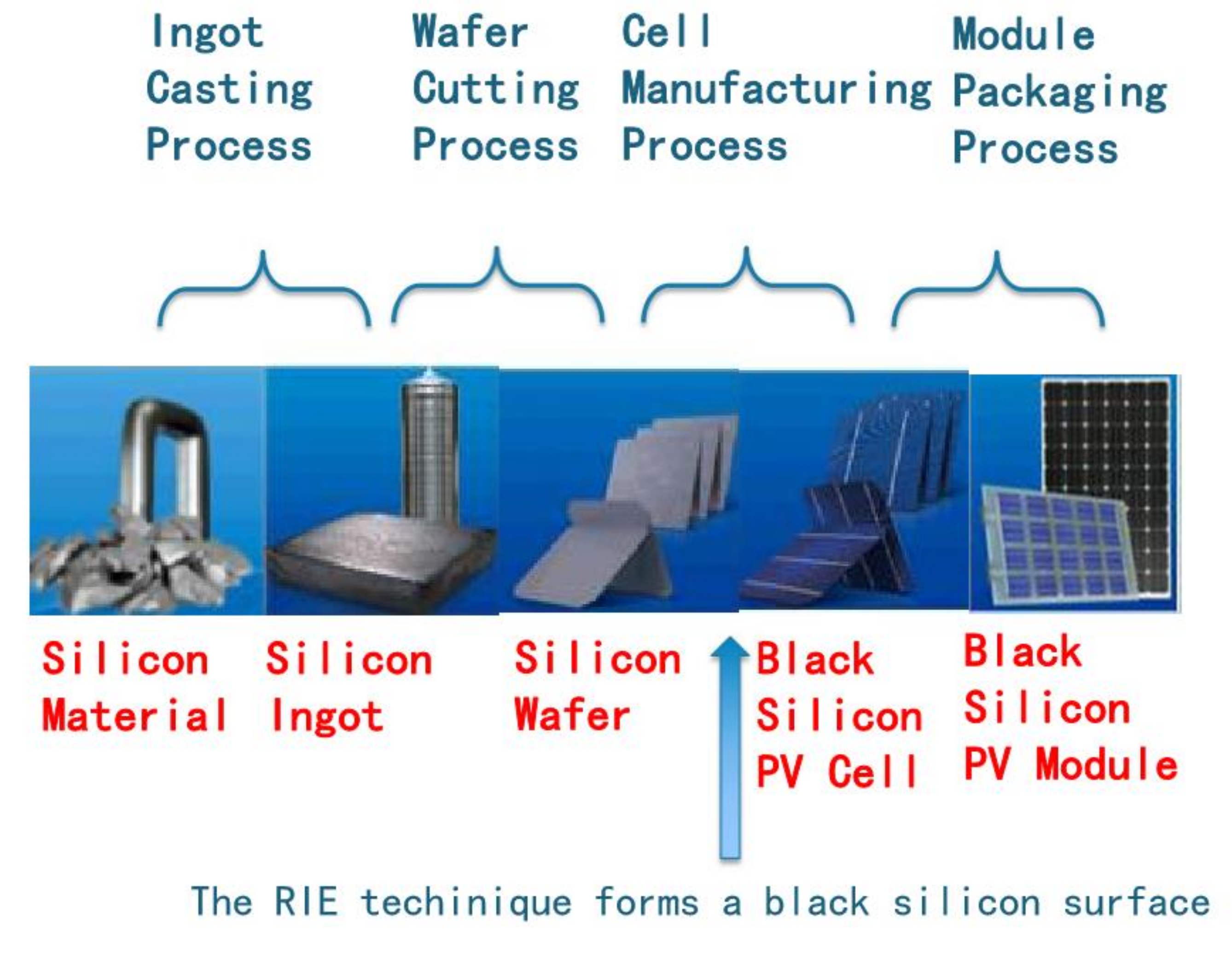
At present, c-Si PV cells mainly include p-Si PV cells and m-Si PV cells. It can be found that both p-Si and m-Si have attempted to produce black silicon surfaces by the RIE technique in earlier references, such as [7]. With the improvement of the technology, traditional silicon carbide particulate suspension cutting of silicon wafer is replaced by diamond wire cutting, which making the cutting cost of silicon wafer greatly reduced. However, the surface of silicon wafer cut by diamond is smooth and the damage layer is shallow. Due to the good periodicity and anisotropy of m-Si, the surface of the pyramid obtained by alkaline cleaning has a good light-trapping effect. However, for the p-Si PV cell occupying the mainstream of the market, the traditional cleaning cannot match the diamond wire cutting. As a result, the surface does not absorb light well. However, the black silicon surface can obtain a good light-trapping effect, which allows the p-Si to absorb more light. After extensive research, black silicon cell technology has become relatively mature. A benchmark table of the electrical performances of p-Si cells based on a black silicon surface mentioned in the references is shown in 
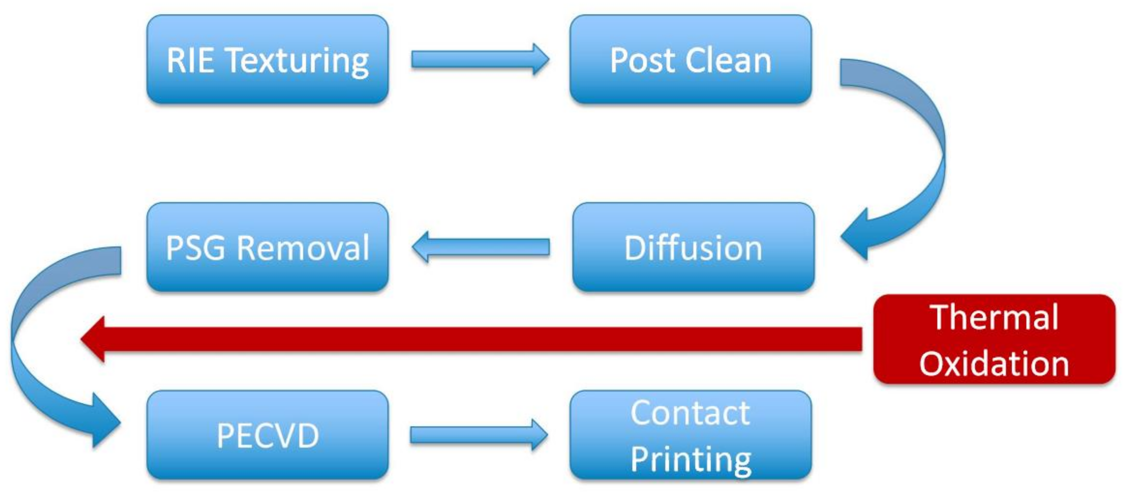
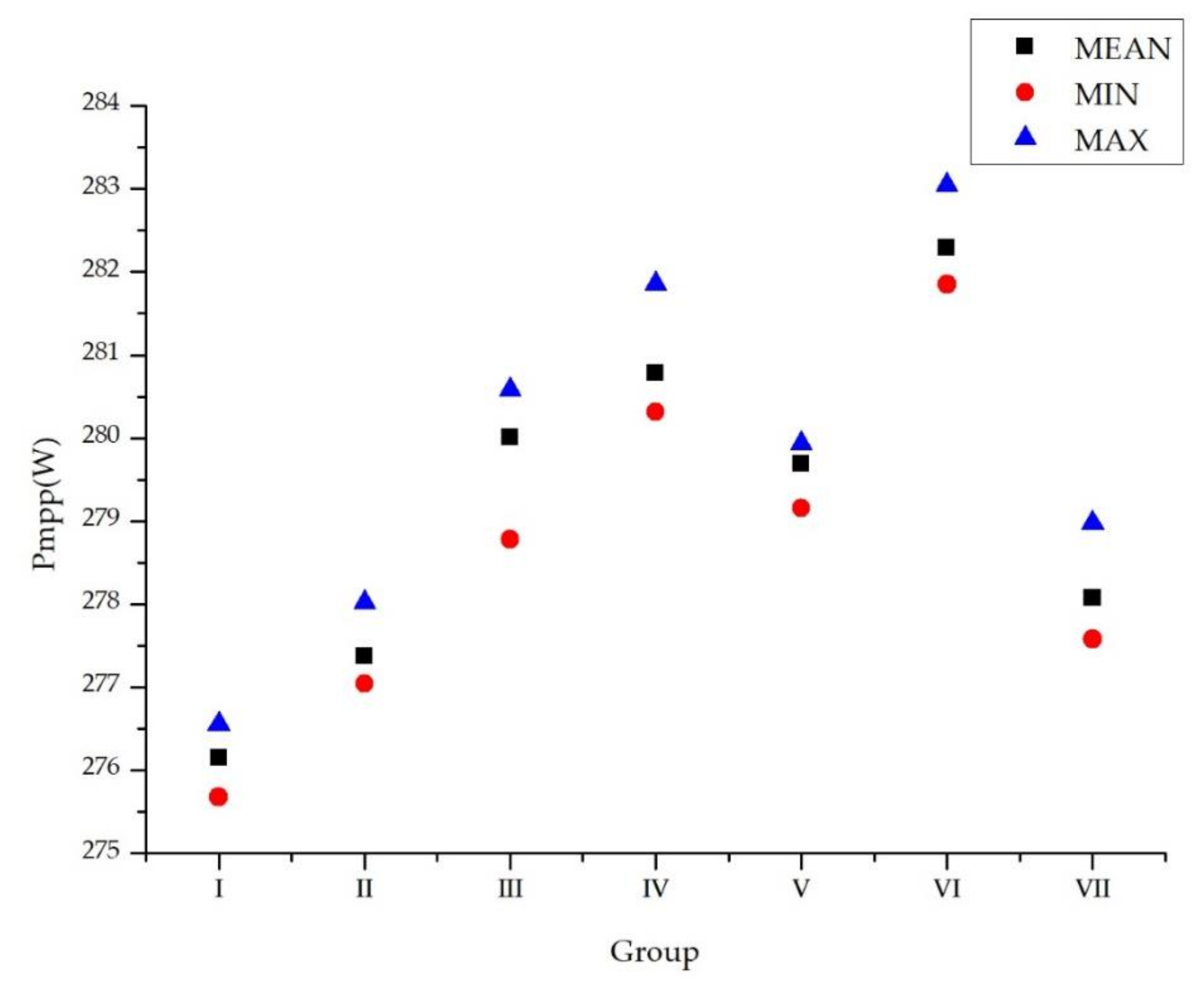
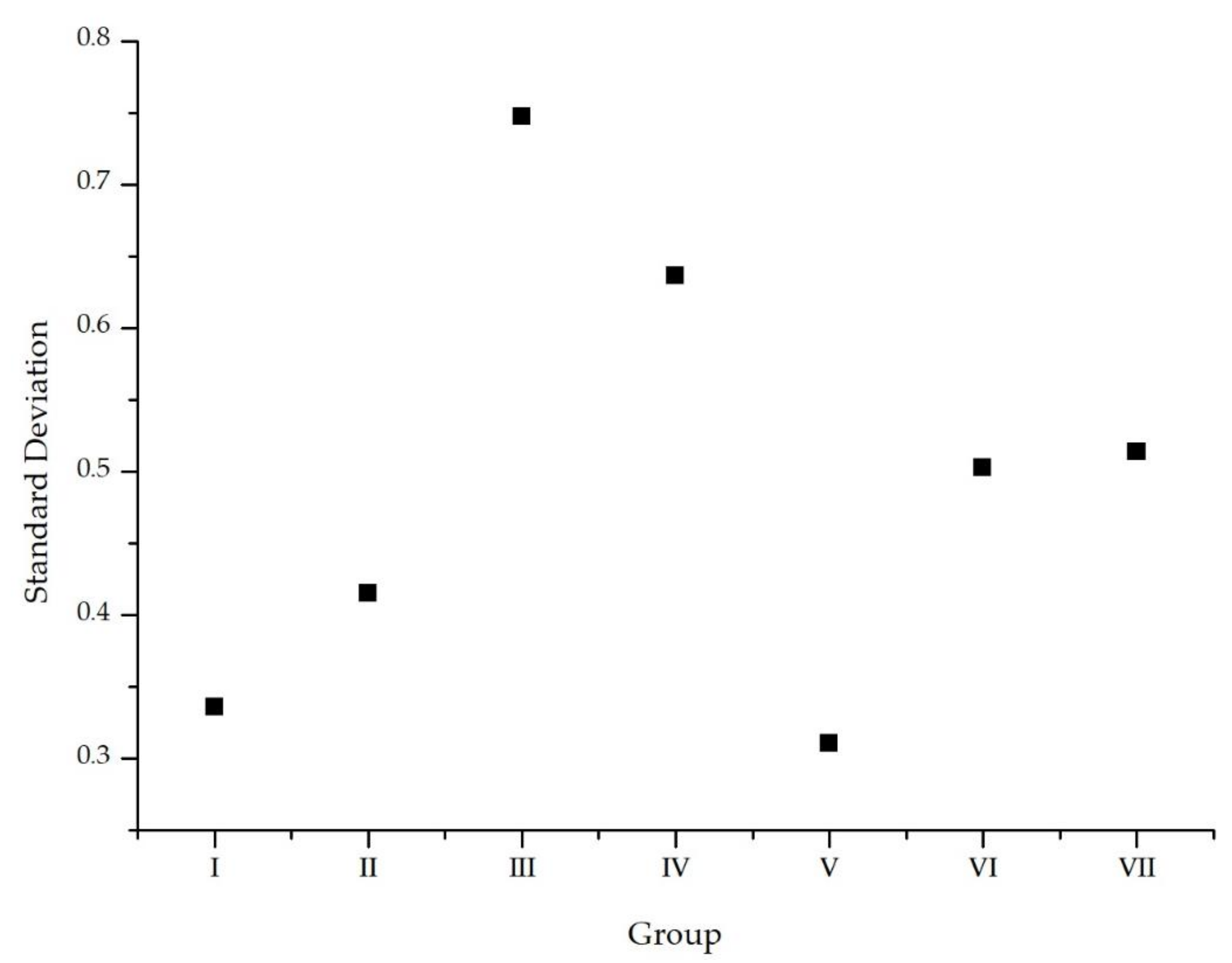
Table 1. Today, the Eff of the mass-produced p-Si PV cells reaches more than 18%. Compared with m-Si PV cells, the production cost of p-Si PV cells is lower. Benefitting from the technological improvements, the maximum Eff of m-Si cells is now around 23%. The Eff of the mass-produced cells is also more than 20%. However, due to the high production cost of m-Si PV cells, their market share is lower than that of p-Si cells with a lower cost. Therefore, in the two technical routes of m-Si and p-Si, p-Si provides a more cost-effective scheme. Some of the technological improvements in m-Si cells can also be applied to p-Si cells. However, due to the defect of the crystalline grain boundary, the profit of p-Si cells will be smaller. Therefore, it is not suitable for p-Si cells to completely copy the related improvements of m-Si cells. Black silicon technology is considered to be an effective way to improve the performances of p-Si cells. According to the references mentioned above, it can be found that the research on black silicon cell technology can be divided into two directions. One direction is surface modification, such as changing the surface condition of the cell or adding some new substances to reconstruct the surface of the cell. It often focuses on the reduction of the reflectivity of the surface of black silicon cells. However, because of the complexity of the entire production process of cells, the reduction of surface reflectivity does not mean the absolute improvement of cells’ performance. Some surface treatments that do not match well with the black silicon surface may even result in a reduction in Eff. The other direction to ensure the overall performance of PV cells is to improve the matching processes of the black silicon surface in PV cells. However, it often pays too much attention to the improvement of a single process, without considering the entire process matching. Therefore, in order to better apply the new technology of the black silicon PV cell from the laboratory to the actual production, this study adopted the black silicon wafer prepared by RIE technology. Furthermore, the overall optimization of the manufacturing processes of PV products through a large number of experiments are discussed in detailed. More importantly, the improvement of matching optimization for black silicon is extended to the module part. By selecting of the pre-cleaning scheme, controlling the thermal oxidation process, and matching components in the module packaging, the performance can be further improved. Our experimental results show that an actual Eff and output power improvement can be achieved, which can be directly used in PV products.

2. Process Improvement Methods

The production of p-Si PV modules in the factory is mainly made by silicon materials, which is completed through four processes: Ingot casting, wafer cutting, cell manufacturing, and module packaging. After the wafer cutting process, the black silicon wafer was prepared by RIE technology, and then the following cell manufacturing and module packaging processes were carried out to form the black silicon PV cells and the black silicon PV modules. The entire production processes of traditional p-Si PV modules and the insertion location of black silicon texturing by the RIE technique are shown in Figure 1. The RIE is the core of the black silicon technology. Nanoscale holes were prepared by bombarding the surface of silicon wafers with SF6 plasma. The reaction equation is Si + SF6 + O2 + Cl2 → SiF4(g) + SiCl4(g) + SiFxOy(s) + SOFx(s). Pre-cleaning and post cleaning were required before and after the RIE process. The RIE equipment used in this study was from Changzhou Bitai Technology Co., Ltd. (Changzhou, China).
The first experiment of this study was the selection of lotions. By comparing the differences of PV cell textures and electrical performances cleaned with different lotions, a more suitable lotion can be obtained. In the process of wafer cutting, diamond wire cutting has been widely used in the silicon wafer, which greatly reduces the cost compared with traditional silicon carbide particulate suspension cutting. However, the surface of the wafer cut in this way is relatively flat, with parallel grooves formed by the diamond wire. Such a surface has poor light absorption. The scanning electron microscope (SEM) images of silicon wafer surfaces formed by different cutting modes are shown in Figure 2, and the parallel grooves formed by diamond wire cutting in the right image can be clearly found. These parallel grooves affect the texturing of black silicon surfaces by the RIE technique. Therefore, the surface needs to be pre-cleaned to remove the surface damage layer and impurities. Since different cleaning methods will lead to different surface shapes of silicon wafers, the choice of lotion is an issue to be considered. The choice of an acidic or alkaline solution will result in different textures and electrical performances of the final PV cells.
The second experiment of this study was the addition of thermal oxidation and the adjustment of oxygen flux at a high temperature. In the manufacturing process of PV cells, the damaged layer is removed through the post cleaning step after RIE texturing while the PN junction is formed by diffusion and phospho-silicate glass (PSG) removal after post cleaning. The antireflective film is then prepared by the plasma enhanced chemical vapor deposition (PECVD) step while the positive and negative electrodes are formed through the electrode contact process. The manufacturing of black silicon cell is completed after the above steps. These steps in the manufacturing process of the c-Si PV cell and the addition location of thermal oxygen are shown in Figure 3. After diffusion and PSG removal, the PN junction has a large number of hanging bonds and crystal defects on its surface because of RIE texturing. In the PECVD step, such a surface would result in severe interface overlap due to the lattice mismatch between nitride silicon compound and black silicon, thus weakening the effect of the antireflective film. According to the construction of the silicon dioxide layer mentioned in [14], the addition of the thermal oxidation step will help to eliminate defects, reduce carrier recombination, match black silicon and nitrogen silicon compound film, reduce the surface reflection, and finally increase the cell Eff. In this experiment, the thermal oxidation wzs mainly carried out by the diffusion furnace. The addition of thermal oxidation step and the control of oxygen flux at high temperature will change the electrical performance parameters of the PV cells. The change caused by different oxygen flux was analyzed to find out the best oxygen flux.
The third experiment of this study focused on the module packaging process. The purpose of the steps were to analyze which types of components in the module can better match the black silicon cells. After obtaining the PV cell, it enters the module packaging process, including the soldering of the cells and the packaging of the module. Benefitting from the high light trapping and low reflection, the black silicon cells have higher Eff, resulting in a higher photo-generated current. Due to the high current, the packaging loss of PV modules made by black silicon cells is high, so it is necessary to study the optimization of module packaging. The main means to reduce the packaging loss of PV modules is to reduce their electrical and optical losses. This experiment was mainly on the selection and matching of various reflective components in welding and packaging, to reduce the packaging loss of black silicon PV modules and obtain optimal packaging scheme. Specifically, the performances of PV modules were optimized according to the selection of glass, ethylene-vinyl acetate copolymer (EVA), back sheet, and soldering strip required for soldering of the cell string in the PV module packaging structure, as shown in Figure 4.
The experiments selected in this study take into account the steps that need to be matched with black silicon in almost the entire production processes of the PV cell and module. Through these comparative experiments, the optimized production scheme was determined to achieve the performance improvements of black silicon cells and modules.

3. Experiments and Results

3.1. The First Experiment and the Results

In the first experiment, two groups (1000 chips per group) of the silicon wafers were pre-cleaned using the corresponding schemes as shown in Table 2. Additionally, the two groups of the silicon wafers were cut from the same silicon ingot at the same position. The difference between the two groups was in the pre-cleaning method. The two groups subsequently adopted the same cell manufacturing process, and introduced a series of control points to ensure the final cells qualified. The unqualified cells were not considered as the results of the experiment. These control points were used to control qualified products in the production of traditional PV modules. The same control points were also used in the last two experiments. The following elements were controlled:
  • The black silicon wafer should have a reflectivity of 12–14% after post cleaning.
  • The cell sheet resistance should be 90–105 Ω/sq. after diffusion.
  • The corrosion thickness of the cell should be 1.5–1.7 μm through PSG removal.
  • The thickness of the antireflective film of the nitride silicon compound through PECVD should be 79–80 nm, and the refractive index should be 2.13–2.14.
  • The surface silver paste consumption in contact printing should be 100–105 mg.
The differences between the two comparison groups were obtained through the first experiment. After pre-cleaning, the appearance difference of the two groups of silicon wafers is shown in Figure 5. Additionally, the appearance difference of the two groups of cells after contact printing is shown in Figure 6. In the experiment, the electrical performances of the two groups of cells, such as open-circuit voltage (Uoc), Isc, short-circuit current density (Jsc), filling factor (FF), and Eff, were measured. The results are shown in Table 3. The standard deviation of the cells Jsc of each group of samples is shown in Figure 7.
The appearances of the black silicon wafers and the electrical performances of the cells in the two groups are obviously different. In group II, the surface texture of black silicon wafers and cells is obvious, and the Isc and Eff are low. In group I, the black silicon wafers and cells have a good appearance consistency, the surface texture is not obvious, and the Isc and Eff are significantly increased compared with group I.

3.2. The Second Experiment and the Results

In the second experiment, the control of the oxygen flux was crucial. The effects of different oxygen flux on the cells’ performance were compared by using four groups (1000 chips per group) of silicon wafers, which were cut from the same silicon ingot in the same position and divided into four groups. The cleaning scheme using HF/HNO3 lotion was used in the pre-cleaning. Then, the black silicon was produced by the RIE technique and the diffusion and PSG removal processes were carried out. Then, it went through the thermal oxidation step to enter the PECVD step. For the samples, group I directly entered PECVD step without thermal oxidation, and group II, III, and IV adopted thermal oxidation. The thermal oxidation was completed by a tubular diffusion furnace. The specific operations are shown in Table 4, including seven operations in total, where A refers to the amount of oxygen flux, and its unit is SCCM.
According to the specific operations in Table 4, for group II, III, and IV, the parameter A is 2000, 2200, and 2500 SCCM, respectively. The four groups subsequently adopted a consistent PECVD step and contact printing step. The electrical performance results and differences of the four groups of black silicon PV cells obtained are shown in Table 5. The standard deviation of the cells’ Jsc of each group of samples is shown in Figure 8.
According to the data shown in Table 5, it can be found that the group without the thermal oxidation step has the lowest electrical performance. This indicates that it is necessary for black silicon cells to insert the thermal oxidation before the PECVD step as expected. An effective silicon dioxide layer formed on the surface of the black silicon cell can eliminate the hanging bonds and crystal defects. It helps to obtain a good antireflection effect after the subsequent PECVD step. Group III showed the highest improvement in Uoc, Isc, and Eff compared with the other groups.

3.3. The Third Experiment and the Results

In the third experiment, how to match the module packaging process with the black silicon cell is an important problem. Here, the cells in group III completed in the second experiment were used directly. According to the standard PV module specifications, one PV module was composed of 60 cells. All the cells were divided into seven groups (five modules per group) for packaging, and each group realized different packaging methods. Different packaging methods are mainly about the selection of components, as shown in Table 6. These components include the glass, the soldering strip on the cell string, the reflective film on the soldering strip, the front EVA, the back EVA, and the back sheet, as mentioned in Figure 4 above. Regarding the selection of glass, coated reinforced glass is generally chosen. Group VI and group VII belong to the type of dual-glass PV module, whose back sheet is replaced by glass. The thickness of glass used in the dual-glass PV module is different from that of the conventional (back sheet) PV module. These two groups also play a role in comparing the matching of the black silicon cell in the dual-glass PV module and conventional PV module. The selection of the soldering strip is mainly between the traditional (flat) soldering strip and the twill soldering strip. The twill soldering strip is a twill structure formed on the copper base of the soldering strip (tin-plated copper strip) to increase the reflected light on the surface, as shown in Figure 9. The reflective film of the solder strip refers to a film coated with reflective material affixed to the surface of the solder strip. When the sunlight shines on the solder strip, it will form multiple reflections between the reflective film and the inner interface of the glass, which may cause the light to shine on the cell again. However, the reflective film can only be attached to the traditional solder strip. Therefore, one of the conclusions to be drawn in this experiment is whether the flat soldering strip, the flat soldering strip with the reflection film, or the twill soldering strip is more suitable for the black silicon cell. In order to make the cell better absorb light, the front EVA is often a highly transparent material, while the back EVA is more suitable to be white or transparent, which is also a question we want to prove. Because of the combination of the above problems, seven comparison groups were needed in the experiment. In addition to the selection of the above materials, the aluminum alloy frame and terminal box do not involve the process of light irradiation of the cell, so they have little effect on the performance of the black silicon cell. In the experiment, the same aluminum alloy frame and terminal box were used to ensure that these components would not cause errors. Group I adopted the traditional module packaging process, as a reference group.
After the packaging experiment, the electrical performance results of the seven groups were obtained, as shown in Table 7, where Impp refers to the current of the maximum power point (Impp) and Umpp refers to the voltage of the maximum power point (Umpp). Pmpp refers to the power of the maximum power point (Pmpp) and, for modules, to their output power.
It can be seen that for the black silicon cell, different components will get different output power, so the packaging loss is different. By comparing the data of group I and II, it can be seen that the white back EVA can achieve a 1.21 W increase in module output power. By comparing the data of group I and III, the output power of the module can be improved by 3.85 W with the reflective film. According to the data comparison of group I and IV, the combination of the white EVA and the reflective film can further improve the output power of the module by 4.62 W. According to the comparison of the data of group IV and V, the output power increment of the twill soldering strip for the module is less than the reflective film. According to the group V and VI data, the output power of the dual-glass module is higher than that of the conventional module. The output power decline of group VII is due to the drift of the reflective film shading the cell after the lamination step. Compared with the normal position of the reflective film of the conventional module, the reflective film of the dual-glass module showed a drift, as shown in Figure 10. The average, maximum, and minimum values of output power of the modules of seven groups are shown in Figure 11. Compared with group I, the output power of the modules of the last groups is improved. Compared with group I, the output power of the modules of group VI increased by the most 6: 13W. Since the data in Table 7 are averaged, error is an issue to consider. The standard deviation of the modules’ output power of each group of samples is shown in Figure 12.

4. Discussion

In the first experiment, it was found that the black silicon wafers of group I had a lesser reflective effect than the black silicon wafers of group II. The black silicon wafers of group I had stronger light-trapping performance, which indicated that the pre-cleaning scheme formed a better match for the preparation of the black silicon surface using the RIE technique and played a more positive role. The black silicon wafers of group II reflected light obviously, indicating that the surface treatment did not achieve a good light-trapping effect. The black silicon of group I absorbed more photons per unit of time because of the stronger light-trapping performance. The higher number of absorbed photons per unit of time mainly causes the increase of the Isc and the Impp, so the Isc of group I cells increased but the Uoc did not change much. According to the formula of Eff, the Eff is improved because the Isc and Impp are increased without increasing the irradiation light intensity. Therefore, in the performance measurement, the cells of the two groups received the same standard light irradiation. The cell surface of group I showed a stronger light-trapping performance and obtained more photons per unit of time, so its Isc and Eff are higher than those of group II. In order to better match the RIE technique to prepare black silicon, HF/HNO3 washing solution should be adopted as the pre-cleaning step.
In the second experiment, the results mainly show the importance of the silicon dioxide layer formed by the thermal oxidation. The silicon oxide layer eliminates the hanging bonds and crystal defects on the silicon wafer surface, which causes a small increase in the Uoc. At the same time, the silicon dioxide buffer layer also matches the nitride silicon compounds well to enhance the antireflection, causing a small increase in Isc, which in fact slightly increases the photons absorbed by the cell per unit of time. The optimal oxygen flux at 2200 SCCM was found in the experiment. However, thermal oxidation requires a certain production cost, so the cost factor of thermal oxidation should be fully considered in the actual production to decide whether to insert this step.
In the third experiment, with the change of the component selection, the more optical benefits the black silicon cell in the module can obtain, the greater the Isc and the output power. Specifically, the addition of the reflective film and twill soldering strip will provide more optical benefits, and the use of white EVA will also provide optical benefits. In conventional PV modules, the optical benefit of the reflective film is higher than that of the twill soldering strip. However, in the case of the dual-glass modules, the reflective film drift shades the cell, resulting in the lower output power of group 7 than group 6. This is mainly due to the glass structure on both sides of the dual-glass module, and the internal stress of the module is relatively high., Moreover, the reflective film is partially separated from the soldering strip after lamination, which leads to drift. However, the overall optical income of dual-glass modules is higher than that of conventional modules. Therefore, in the actual production, it is necessary to consider whether to produce conventional modules or dual-glass modules. It is not simply a matter of replacing components but of resetting and debugging the assembly line. The reflective film should be used for the conventional module and the twill soldering strip should be used for the dual-glass module.
To improve the power of photovoltaic modules, reducing the encapsulation loss is an important issue. In addition to the replacement of components adopted in the third experiment, there are other methods that can further reduce package losses and increase component power. One method is to improve the antireflection membrane structure of glass. A double layer of anti-reflection (AR) film can be applied to the glass to improve the transmittance of light of different wavelengths. However, the application of this technology in PV glass is not mature enough. Another way is to enlarge the surface area of the cell. Increasing the light area can increase the photogenerated current, thus increasing the output power. However, increasing the area of the cell makes the PV cell more fragile. The fragmentation rate during production will increase. The production cost will increase. Large area PV cells are difficult to mass produce at present.
The overall purpose of our experiments is to improve the electrical performance of the PV cell and module in standard production. However, there are always some limitations that hinder the further exploration. Firstly, the deadliest of these is photoelectric conversion efficiency. The photoelectric conversion efficiency in solar energy equipment is much lower than the photothermal conversion efficiency. This makes it difficult to improve the electrical performance of PV power generation. Secondly, the mass production of the improved product requires a complicated quality control process. Lastly, production costs tend to limit the use of new technologies.
Due to the large number of samples in the three different experiments in this study, in addition to the conventional error analysis, the defective products were screened out in the first two experiments. For mass production, it is necessary to screen the cells. The defective index is also shown in Table 3 and Table 5. According to the control of process elements, we excluded unqualified samples, which greatly reduced the error caused by the experiment. It can be found that the errors of the first two experiments are relatively low. Due to the quality control of the cell samples, all the module samples in the third experiment were qualified.

5. Conclusions

In this paper, three experiments were carried out to analyze the improvement of the production scheme to match the black silicon surface, including the selection of lotion in the pre-cleaning step, the control of oxygen flux in the thermal oxidation step, and the selection of components in the module packaging process. The first experiment showed that using HF/HNO3 lotion could better match the subsequent RIE technique to produce black silicon wafer. The black silicon wafer produced by this scheme has a higher light trapping, so that the electrical performance of the black silicon cell made from it can be enhanced. As a result, the Eff can be improved by nearly 0.154%. The second experiment showed that the thermal oxidation step is necessary for making the black silicon cell. It was found that the black silicon cell has the highest electrical performance when the oxygen flux at 2200 SCCM, and the Eff can be improved by 0.11% compared with the cell without the thermal oxidation step. The third experiment showed that the dual-glass black silicon PV modules with a twill soldering strip can achieve 6.13 W in an output power increase compared with conventional black silicon PV modules. In this study, the selection of acid lotion in the pre-cleaning step, the addition and control of the thermal oxidation step in the cell manufacturing process, and the reasonable selection of components in the module packaging process were proposed to realize the improvement of the black silicon PV cell and module electrical performances, especially the improvement of the module output power. It provides meaningful guidance and suggestions for the production process research of black silicon PV products in PV enterprises.

Author Contributions

Z.C. covered all the research of this study. Z.C. and Y.Z. designed the experimental scheme. Z.C. and H.G. wrote the paper. H.J. and L.F. collected the experimental data. H.Z. and B.C. analyzed the experimental data. Z.C. and S.W. revised the paper. All authors have made great efforts in this research work. All authors have read and agreed to the published version of the manuscript.

Funding

This research was supported by Tianjin Technical Expert Project under grant 19JCTPJC42700; the Science and Technology Planning Project of Jin Nan District Tianjin under grant 20190111; University-level research project of Tianjin Sino-German University of Applied Sciences under grants zdkt2018-001, zdkt2018-002, zdkt2019-018.

Acknowledgments

The authors sincerely acknowledge much help and support from their institutions, especially Tianjin Yingli new energy Co., Ltd. The experimental samples and most of measurements are provided by Tianjin Yingli new energy Co., Ltd.

Conflicts of Interest

The authors declare no conflict of interest.

References

  1. Chapin, D.M.; Fuller, C.S.; Pearson, G.L. A New Silicon p-n Junction Photocell for Converting Solar Radiation into Electrical Power. J. Appl. Phys. 1954, 25, 676–677. [Google Scholar] [CrossRef]
  2. Green, M.A. The Path to 25% Silicon Solar Cell Efficiency: History of Silicon Cell Evolution. Prog. Photovolt. Res. Appl. 2009, 17, 183–189. [Google Scholar] [CrossRef]
  3. Jansen, H.; Boer, M.D.; Legtenberg, R.; Elwenspoek, M. The black silicon method: a universal method for determining the parameter setting of a fluorine-based reactive ion etcher in deep silicon trench etching with profile control. J. Micromech. Microeng. 1995, 5, 115–120. [Google Scholar] [CrossRef] [Green Version]
  4. Her, T.H.; Finlay, R.J.; Wu, C.; Deliwala, S.; Mazur, E. Microstructuring of silicon with femtosecond laser pulses. Appl. Phys. Lett. 1998, 73, 1673–1675. [Google Scholar] [CrossRef]
  5. Schnell, M.; Ludemann, R.; Schaefer, S. Plasma surface texturization for multicrystalline silicon solar cells. In Proceedings of the 28th IEEE Photovoltaic Specialists Conference, Anchorage, AK, USA, 15–22 September 2000. [Google Scholar]
  6. Wu, C.; Crouch, C.H.; Zhao, L.; Carey, J.E.; Younkin, R.; Levinson, J.A.; Mazur, E.; Farrell, R.M.; Gothoskar, P.; Karger, A. Near-unity below-band-gap absorption by microstructured silicon. Appl. Phys. Lett. 2001, 78, 1850–1852. [Google Scholar] [CrossRef]
  7. Yoo, J.S.; Parm, I.O.; Gangopadhyay, U.; Kim, K.; Dhungel, S.K.; Mangalaraj, D.; Yi, J. Black silicon layer formation for application in solar cells. Sol. Energy Mater. Sol. Cells 2006, 90, 3085–3093. [Google Scholar] [CrossRef]
  8. Yoo, J.S. Reactive ion etching (RIE) technique for application in crystalline silicon solar cells. Sol. Energy 2010, 84, 730–734. [Google Scholar] [CrossRef]
  9. Toor, F.; Branz, H.M.; Page, M.R.; Jones, K.M.; Yuan, H.C. Multi-scale surface texture to improve blue response of nanoporous black silicon solar cells. Appl. Phys. Lett. 2011, 99, 103501. [Google Scholar] [CrossRef]
  10. Liu, B.; Zhong, S.; Liu, J.; Xia, Y.; Li, C. Silicon Nitride Film by Inline PECVD for Black Silicon Solar Cells. Int. J. Photoenergy 2012, 2012, 10178–10182. [Google Scholar] [CrossRef]
  11. Cho, C.; Kong, D.; Oh, J.H.; Kim, B.; Lee, B.; Lee, J. Surface texturing method for silicon solar cell using reactive ion etching with metal mesh. Phys. Status Solidi 2015, 211, 1844–1849. [Google Scholar] [CrossRef]
  12. Chen, H.Y.; Lu, H.L.; Ren, Q.H.; Zhang, Y.; Yang, X.F.; Ding, S.J.; Zhang, D.W. Enhanced photovoltaic performance of inverted pyramid-based nanostructured black-silicon solar cells passivated by an atomic-layer-deposited Al2O3 layer. Nanoscale 2015, 7, 15142–15148. [Google Scholar] [CrossRef] [PubMed]
  13. Chen, W.H.; Hong, F.C.N. 0.76% absolute efficiency increase for screen-printed multicrystalline silicon solar cells with nanostructures by reactive ion etching. Sol. Energy Mater. Sol. Cells 2016, 157, 48–54. [Google Scholar] [CrossRef]
  14. Li, P.; Wei, Y.; Tan, X.; Li, X.; Wang, Y.; Zhao, Z.; Yuan, Z.; Liu, A. Effective optimization of emitters and surface passivation for nanostructured silicon solar cells. RSC Adv. 2016, 6, 104073–104081. [Google Scholar] [CrossRef]
  15. Pasanen, T.P.; Laine, H.S.; Ville, V.; Salo, K.; Husein, S.; Savin, H. Impact of Standard Cleaning on Electrical and Optical Properties of Phosphorus-Doped Black Silicon. IEEE J. Photovolt. 2018, 8, 1–6. [Google Scholar] [CrossRef]
  16. Ramosa, C.; Verduzco-Lópeza, Y.; Álvarez-Macíasb, C.; Sanchez-Juarezc, A.; Dutta, A.; Santanaa, G. A new passivation scheme for the performance enhancement of black silicon solar cells. Mater. Today Commun. 2019, 20, 100556. [Google Scholar] [CrossRef]
Figure 1. The production processes of the black silicon PV module.
Crystals 10 00753 g001
Figure 2. The SEM images of silicon wafer surfaces formed by silicon carbide particle suspension cutting (a) and diamond wire cutting (b).
Crystals 10 00753 g002
Figure 3. The manufacturing process of the c-Si PV cell and the addition location of thermal oxygen.
Crystals 10 00753 g003
Figure 4. The PV module packaging structure.
Crystals 10 00753 g004
Figure 5. The appearance comparison diagram of black silicon wafers after pre-cleaning.
Crystals 10 00753 g005
Figure 6. The appearance comparison diagram of black silicon cells.
Crystals 10 00753 g006
Figure 7. The standard deviation of the cells Jsc of two groups.
Crystals 10 00753 g007
Figure 8. The standard deviation of the cells’ Jsc of four groups.
Crystals 10 00753 g008
Figure 9. The schematic diagram of the twill soldering strip.
Crystals 10 00753 g009
Figure 10. The normal reflective film position (left) of the conventional module and the reflective film drift (right) of the dual-glass module.
Crystals 10 00753 g010
Figure 11. The output power of the seven groups.
Crystals 10 00753 g011
Figure 12. The standard deviation of the output power of the modules of the seven groups.
Crystals 10 00753 g012
Table 1. Different black silicon PV cells and their electrical performance analysis.
ReferencesTechniquesLight AbsorptionEff
[6]Femtosecond laser90%*
[7]RIE*10.2%
[8]RIE79.22%16.12%
[9]Metal-assisted etching57–71%17.1%
[10]Plasma immersion ion implantation93%16.25%
[11]RIE90–93%13.11%
[12]atomic-layer-deposition*14.2%
[13]RIE90–98%17.97%
[14]Metal-assisted wet-chemicaletching96.3%18.5%
[15]Deep reactive ion etching96.7–99.1%*
* It is not mentioned in the references.
Table 2. The different cleaning schemes in the pre-cleaning step and subsequent steps.
GroupLotionCleaning TimeCleaning Equipment
IHF: HNO3 (50:550 g/L)50 sThe chain cleaning machine
IIKOH (90 g/L)50 sThe tank cleaning machine
Table 3. The electrical performance results for different groups.
GroupUoc (V)Isc (A)Jsc (mA/cm2)FF (%)Eff (%)Defective Index (%)
I0.6319.190 37.4181.102 19.012 0.27%
II0.6309.102 37.0481.117 18.858 1.32%
Difference value (I-II)0.0010.0880.39−0.0150.154
Table 4. The specific operations of thermal oxidation.
OperationDuration (s)Temperature (℃)Nitrogen Flux (SCCM)Oxygen Flux (SCCM)Action of Diffusion Furnace
11065015,0000Closed
280065015,0000Cell entry
390065015,0000Closed
4120065013,000AClosed
510065013,8000Closed
668065015,0000Cell exit
71065015,0000Closed
Table 5. The electrical performance results and differences of the four groups.
GroupUoc (V)Isc (A)Jsc (mA/cm2)FF (%)Eff (%)Defective Index (%)
I (No thermal oxidation)0.63049.170537.3380.7018.990.30%
II (A = 2000 sccm)0.63149.182137.3780.7519.050.29%
III (A = 2200 sccm)0.63179.213137.5080.6519.100.31%
IV (A = 2500 sccm)0.63169.208137.4880.5519.070.30%
Difference value (II-I)0.00110.01160.040.050.06
Difference value (III-I)0.00130.04260.17−0.050.11
Difference value (IV-I)0.00120.03760.15−0.150.08
Table 6. The seven groups formed by different components.
GroupGlassSoldering StripReflective FilmFront EVABack EVABack Sheet
I3.2 mm 1.0 × 0.25 flat nonetransparenttransparentKPE
II3.2 mm 1.0 × 0.25 flat nonetransparentwhiteKPE
III3.2 mm 1.0 × 0.25 flat 1.2 mmtransparenttransparentKPE
IV3.2 mm 1.0 × 0.25 flat 1.2 mmtransparentwhiteKPE
V3.2 mm 1.0 × 0.25 twill nonetransparentwhiteKPE
VI2.5 mm Semi-tempered1.0 × 0.25 twillnonetransparentwhite2.5 mm Semi-tempered
VII2.5 mm Semi-tempered1.0 × 0.25 flat1.2 mmtransparentwhite2.5 mm Semi-tempered
Table 7. The electrical performance results of the seven groups.
GroupUoc (V)Isc (A)Umpp (V)Impp (A)Pmpp (W)FF (%)Packaging Loss (%)Power Increment Relative to Group I (W)
I38.2819.48331.0908.882276.1676.072.18%0.00
II38.3059.51531.0848.923277.3776.101.75%1.21
III38.3099.63031.0499.018280.0075.900.82%3.85
IV38.3269.63131.0419.045280.7876.060.54%4.62
V38.3099.55831.1798.971279.6976.380.93%3.54
VI38.3279.62731.2749.026282.2976.510.01%6.13
VII38.3139.50331.2758.891278.0776.381.51%1.91

