Article

Crystal-Plane Dependence of Nb-Doped Rutile TiO2 Single Crystals on Photoelectrochemical Water Splitting

Advanced Coating Technology Research Center, National Institute of Advanced Industrial Science and Technology, Tsukuba Central 5, 1-1-1 Higashi, Tsukuba, Ibaraki 305-8565, Japan
*
Author to whom correspondence should be addressed.
Catalysts 2019, 9(9), 725; https://doi.org/10.3390/catal9090725
Submission received: 29 July 2019 / Revised: 14 August 2019 / Accepted: 23 August 2019 / Published: 28 August 2019

Abstract

:
The crystal-plane dependence of the photoelectrochemical (PEC) water-splitting property of rutile-structured Nb-doped TiO2 (TiO2:Nb) single-crystal substrates was investigated. Among the crystal planes, the (001) plane was a very promising surface for attaining good photocurrent. Under 1 sun illumination at 1.5 V vs. a reversible hydrogen electrode, the TiO2:Nb(001) single-crystal substrate showed the highest photocurrent (0.47 mA/cm2) among the investigated substrates. The doped Nb ions were segregated inward from the top surface, and the TiO2 ultrathin layer was formed at the surface of the crystal, resulting in the formation of a heterointerface between the TiO2 and the TiO2:Nb. The enhancement of the PEC properties of the TiO2:Nb(001) single-crystal substrate originated from favorable atomic configurations for water molecule absorption and facilitation of transport of photoexcited electron–hole pairs in the depletion layer formed around the heterointerface of TiO2 thin layers on the base crystal.

Graphical Abstract

1. Introduction

Photoelectrochemical (PEC) reactions have been widely studied, especially for solar hydrogen production and water purification [1,2,3,4,5]. To improve the performance of PEC cells, the development of photoelectrodes with high activity under an excitation light is critical. Photoelectrodes for PEC reactions are usually composed of semiconductor layers and conducting bottom electrodes. Several key factors favor the improvement of photoelectrodes: (1) A large optical absorption and active surface area [6,7], (2) the effective adsorption of reactants onto the photoelectrode surface [8,9], (3) good excited charge separation [10], and (4) efficient excited charge transfer to the bottom electrodes [11,12,13]. Among these key factors, we focused on the properties of the crystal surface to attain new insights into the surface adsorption of reactants and photocarrier transport properties. In the case of crystal-plane surface dependence, numerous reports on crystal-facet-growth nanomaterials have appeared in the literature, and the role of each crystal plane in PEC reactions has been discussed [14,15,16,17].
In the present study, we investigated the PEC reaction of Nb-doped rutile TiO2 (TiO2:Nb) single-crystal substrates with (001), (100), (110), (101), and (111) crystal surfaces to clearly reveal the crystal-plane dependence of the photoelectrodes. TiO2:Nb has been reported as a conductive material that exhibits photocatalytic and PEC reaction properties [18,19,20,21]. For such TiO2:Nb crystals, we first revealed the formation of a heterointerface between the TiO2 ultrathin layer and the Nb-doped base single crystal via segregation of doped Nb ions inward from the top surface; we then investigated the potential significance of the (001) surface plane of the TiO2:Nb crystals on their PEC properties.

2. Results and Discussion

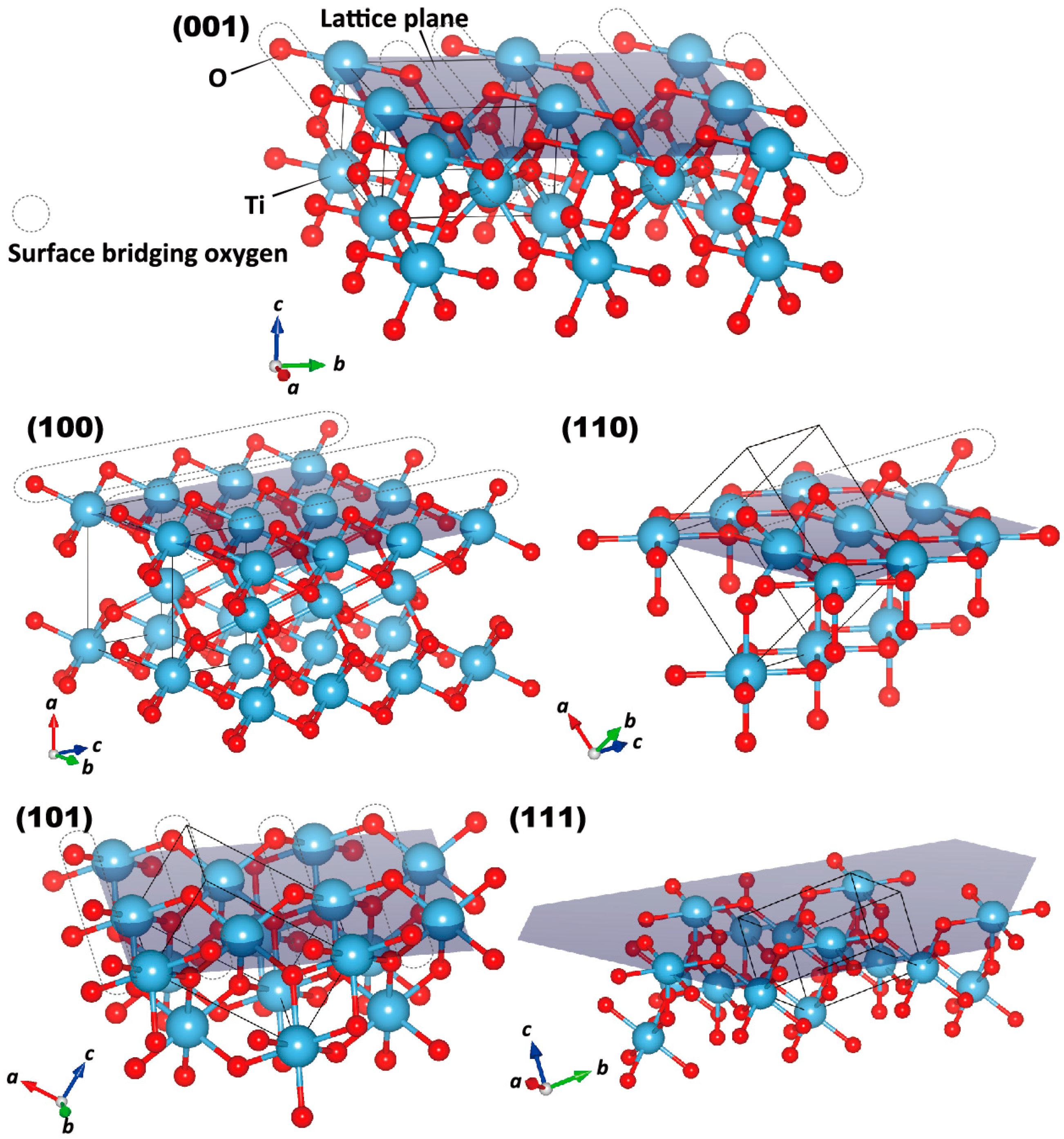
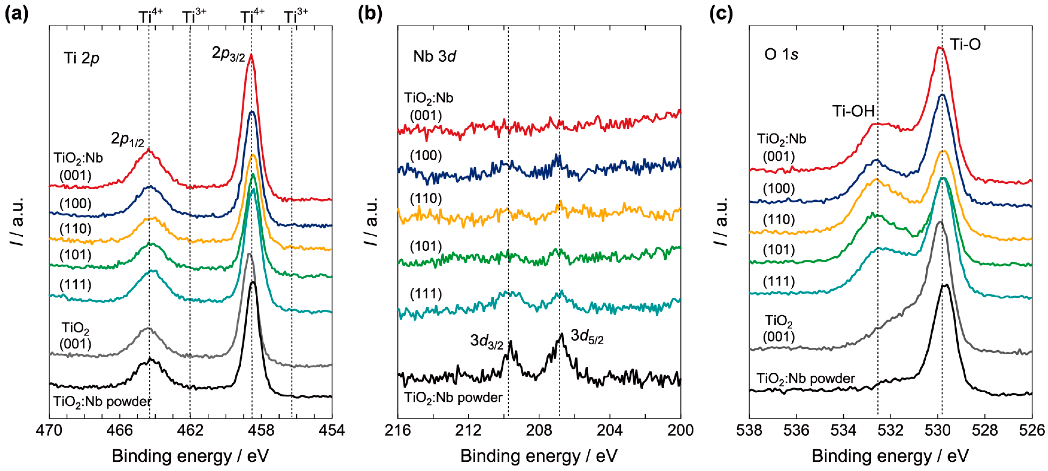
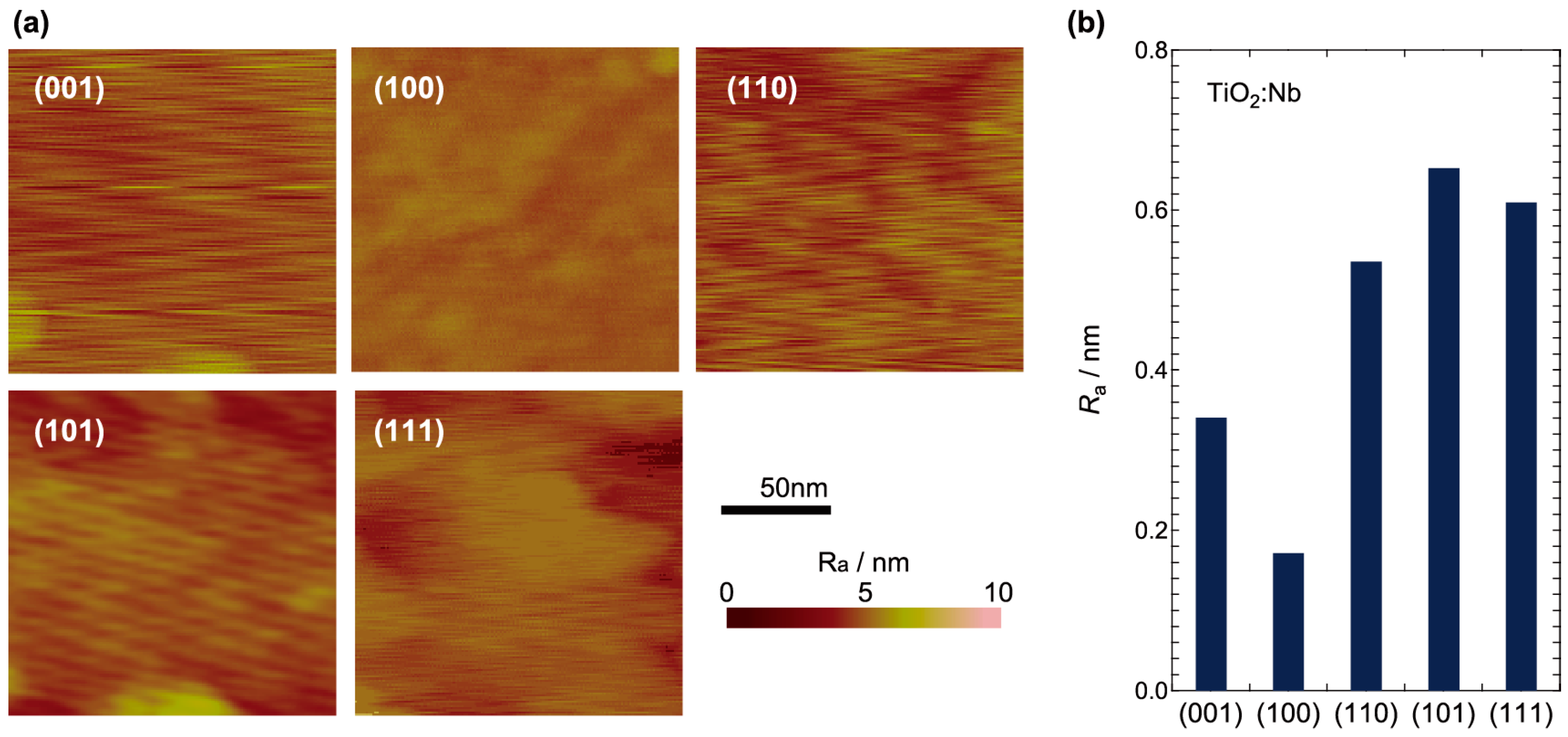
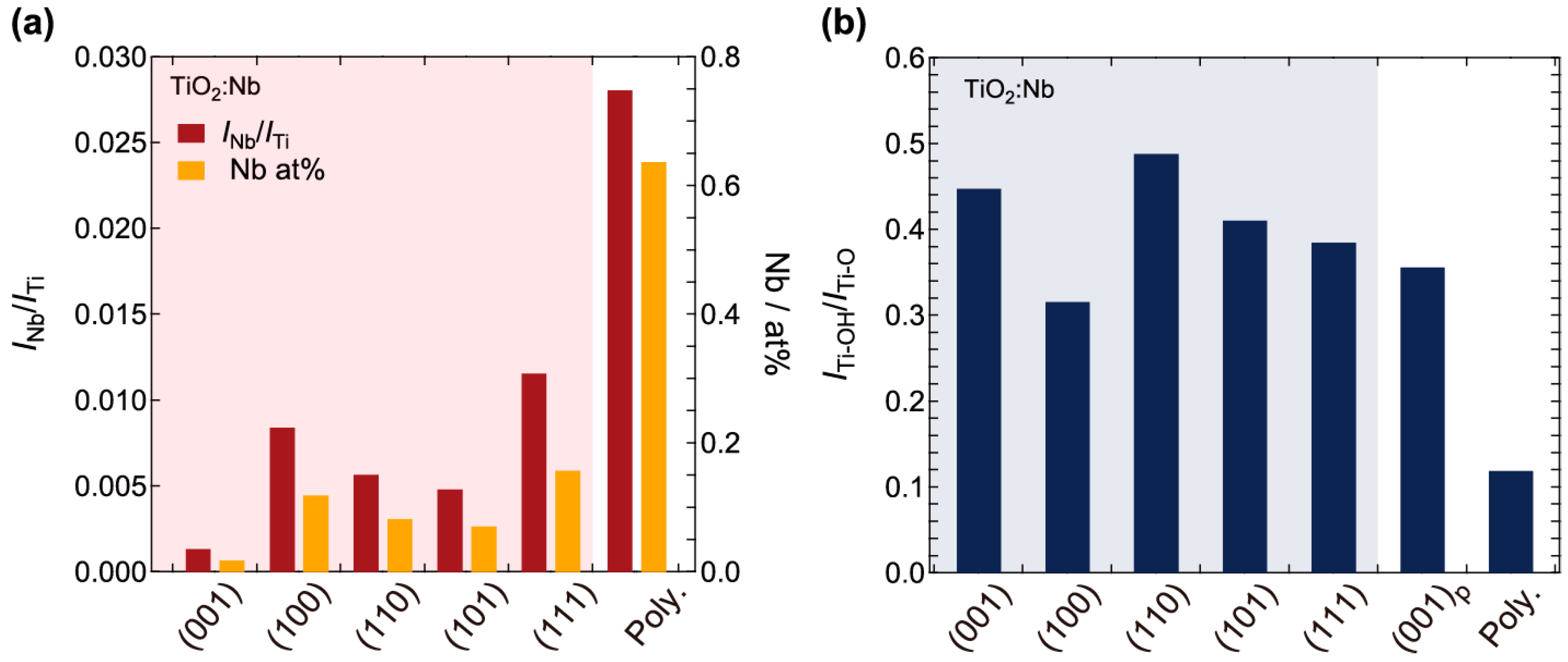
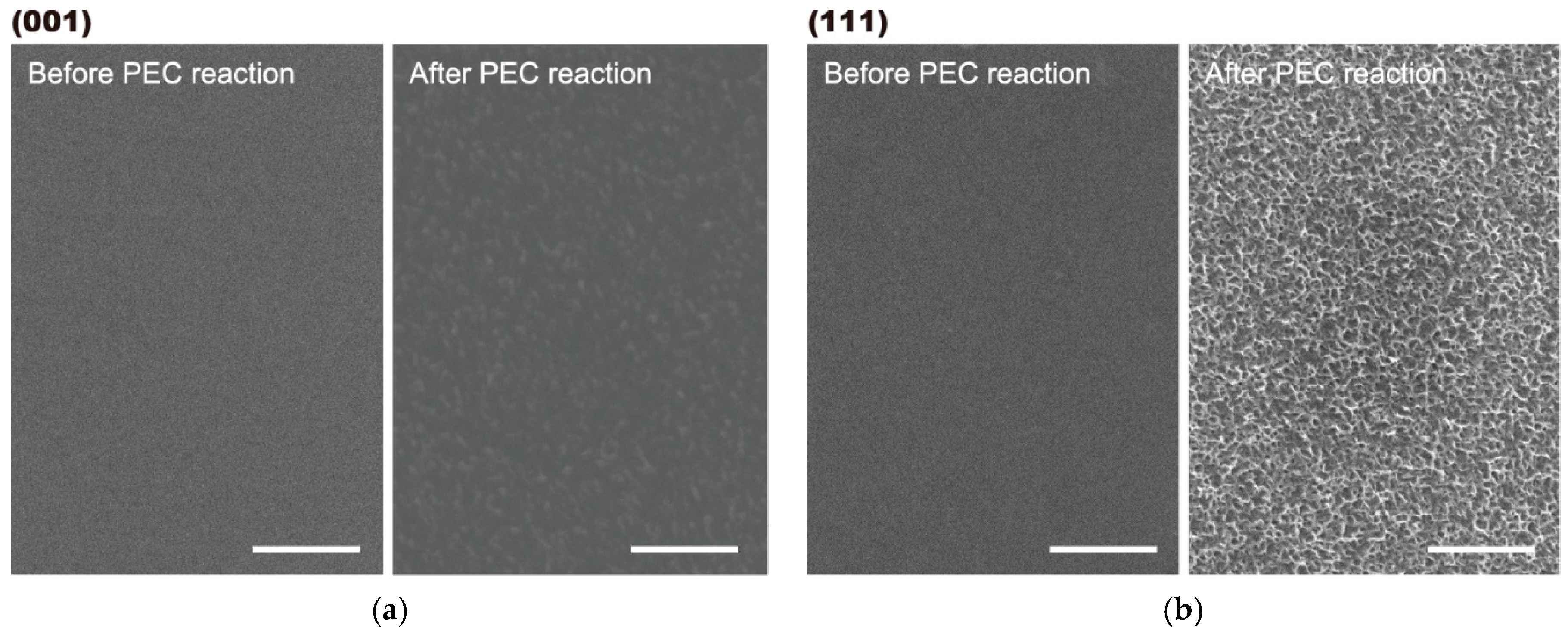
2.1. Surface Analysis

Figure 1 shows the schematic crystal structures of different crystal lattice plane surfaces of rutile TiO2:Nb [22]. The polished surfaces of the as-purchased single-crystal substrates were very flat; their surface roughness (Ra) was evaluated to be ca. 0.17–0.65 nm within a 150 nm square, as shown in the atomic force microscopy (AFM) images in Figure 2. Because the TiO2:Nb single-crystal substrates could not be annealed at high temperatures to preserve their conductivity as a bottom electrode, their surface morphology was not optimized to an atomic step-terrace structure. However, the crystals were cut parallel to each crystal plane within 0.5° accuracy, and we confirmed that the Ra values were sufficiently low.
Figure 3 shows the X-ray photoelectron spectroscopy (XPS) spectra of the Ti 2p, Nb 3d, and O 1s core levels for the TiO2:Nb single-crystal substrates and reference materials (a pure TiO2(001) single-crystal substrate and a TiO2:Nb2O5 (0.43 at% Nb) polycrystalline powder composite). The observed Ti 2p core-level spectra of both TiO2:Nb single-crystal substrates show two peaks at 458.5 (Ti 2p3/2) and 464.4 eV (Ti 2p1/2) (Figure 3a). These peak positions are approximately coincident with those of the pure TiO2 and TiO2:Nb2O5 composite references with Ti4+ ions in their lattice [23,24,25]. The observed Ti 2p3/2 and Ti 2p1/2 peaks in the spectra of the TiO2:Nb single crystals were not shifted to the lower-energy side and broadened compared with the peaks in the spectrum of the TiO2 reference. These results indicate that the Ti ions at the top surface of the TiO2:Nb single crystals were not trivalent ions resulting from the Nb5+ doping in the lattice, but were rather tetravalent ions remaining from undoped TiO2. The Nb 3d spectra of the TiO2:Nb similarly support the tetravalent state of surface Ti ions (Figure 3b). The two typical Nb 3d peaks (3d3/2 and 3d5/2) corresponding to the Nb5+ ions were very small in the spectra of the TiO2:Nb single-crystal substrate surfaces, although these peaks were observed in the spectrum of the TiO2:Nb2O5 (0.43 at% Nb) polycrystalline powder reference. With respect to the relative intensity ratio between the Nb 3d3/2 and Ti 2p3/2 and the calculated Nb content for each sample, the Nb signal in the spectra of the TiO2:Nb single-crystal substrates was obviously small compared with that in the spectra of the TiO2:Nb2O5 powder reference (Figure 4a). XPS analysis is a highly surface-sensitive technique and usually analyzes within a depth 0–10 nm from the top surface. For the whole single crystals of TiO2:Nb, the doped Nb amount was evaluated to be 0.43 at% by X-ray fluorescence analysis. Therefore, we considered that the doped Nb ions at the top surface diffused inside the crystal in association with the valence conversion from Ti3+ to Ti4+ for Ti ions around the Nb ions because of surface oxidation immediately after the cutting and polishing of the surface of the substrates. This diffusion resulted in the formation of a gradual heteroepitaxial interface between the ultrathin TiO2 layer (<10 nm) and the TiO2:Nb at the top surface of the TiO2:Nb single crystals.
Figure 3c shows the O 1s core-level XPS spectra of the TiO2:Nb single crystals and the references. The main peak corresponding to the Ti–O bond was confirmed at 529.8 eV in the spectrum of each sample. Additionally, a broad peak was also observed at approximately 532.3 eV, which can be deconvoluted to two peaks at 531.7 eV and 532.5 eV attributed to Ti–OH bonding and physisorbed water molecules, respectively [23,24,26,27]. The Ti–OH hydroxyl groups on the rutile TiO2 surface make the energy level 0.7 eV below the valence band of the TiO2. This OH group on the surface was energetically stable and could not be oxidized easily by the valence-band holes. Thus, the surface OH groups could be easily stimulated for surface adsorption, functioning as reaction sites. As shown in Figure 4b, the intensity ratio of the Ti–OH to Ti–O peaks in the XPS spectra of the single-crystal substrates was much larger than that in the spectra of the powder reference.

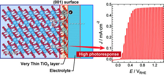
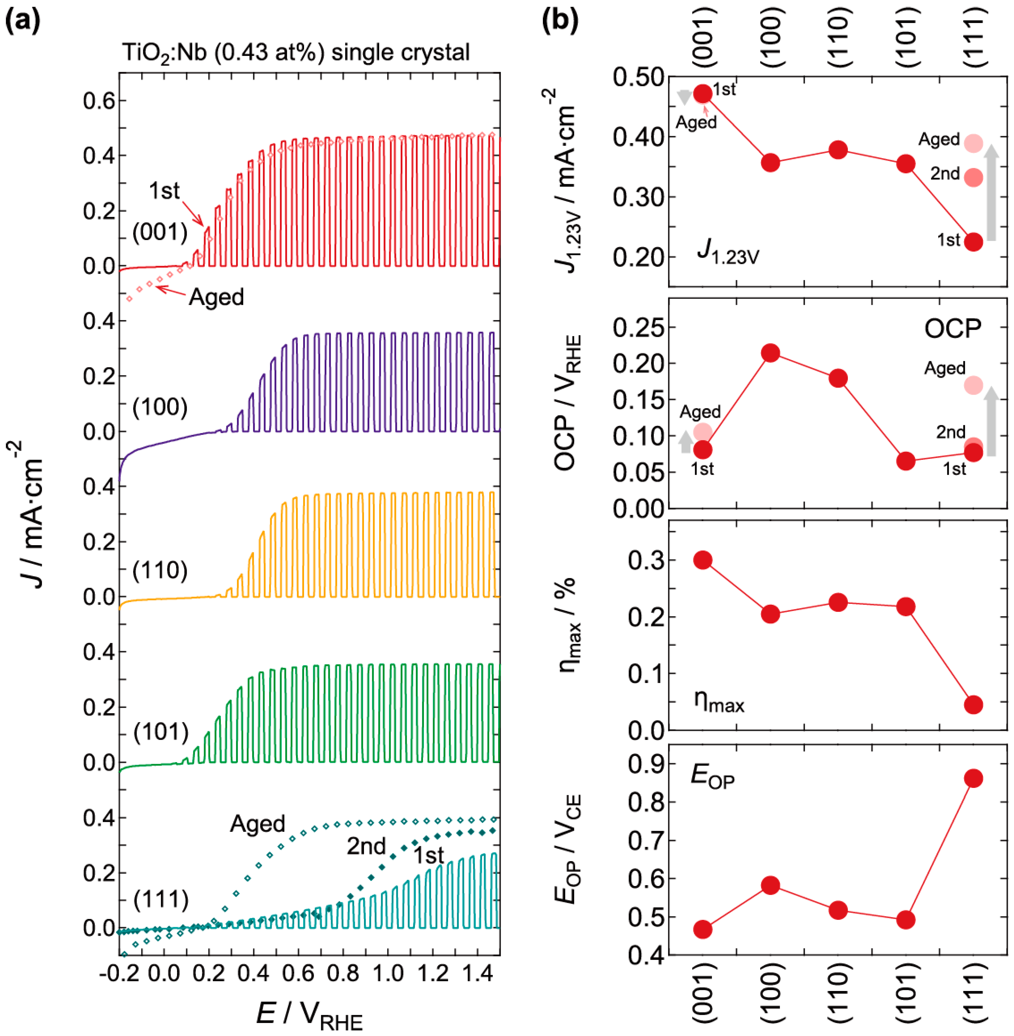
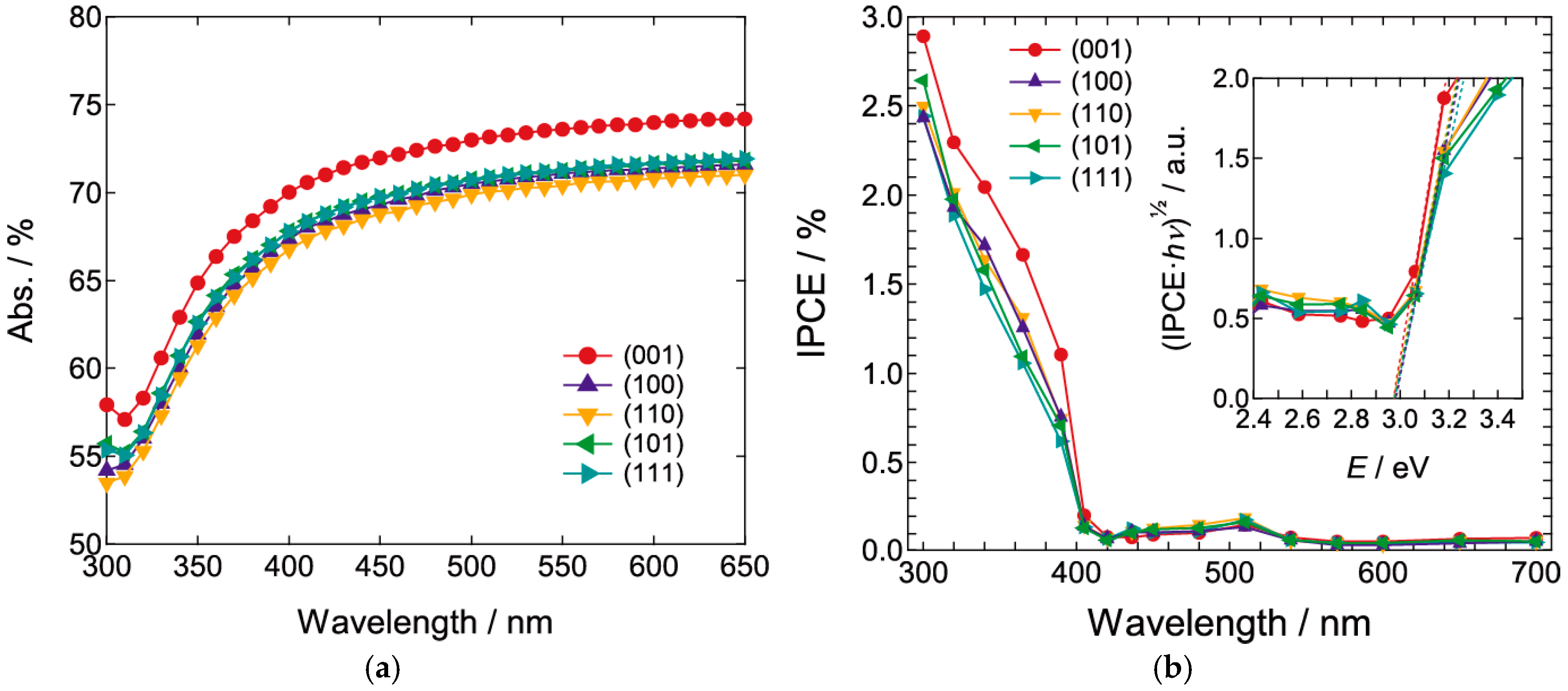
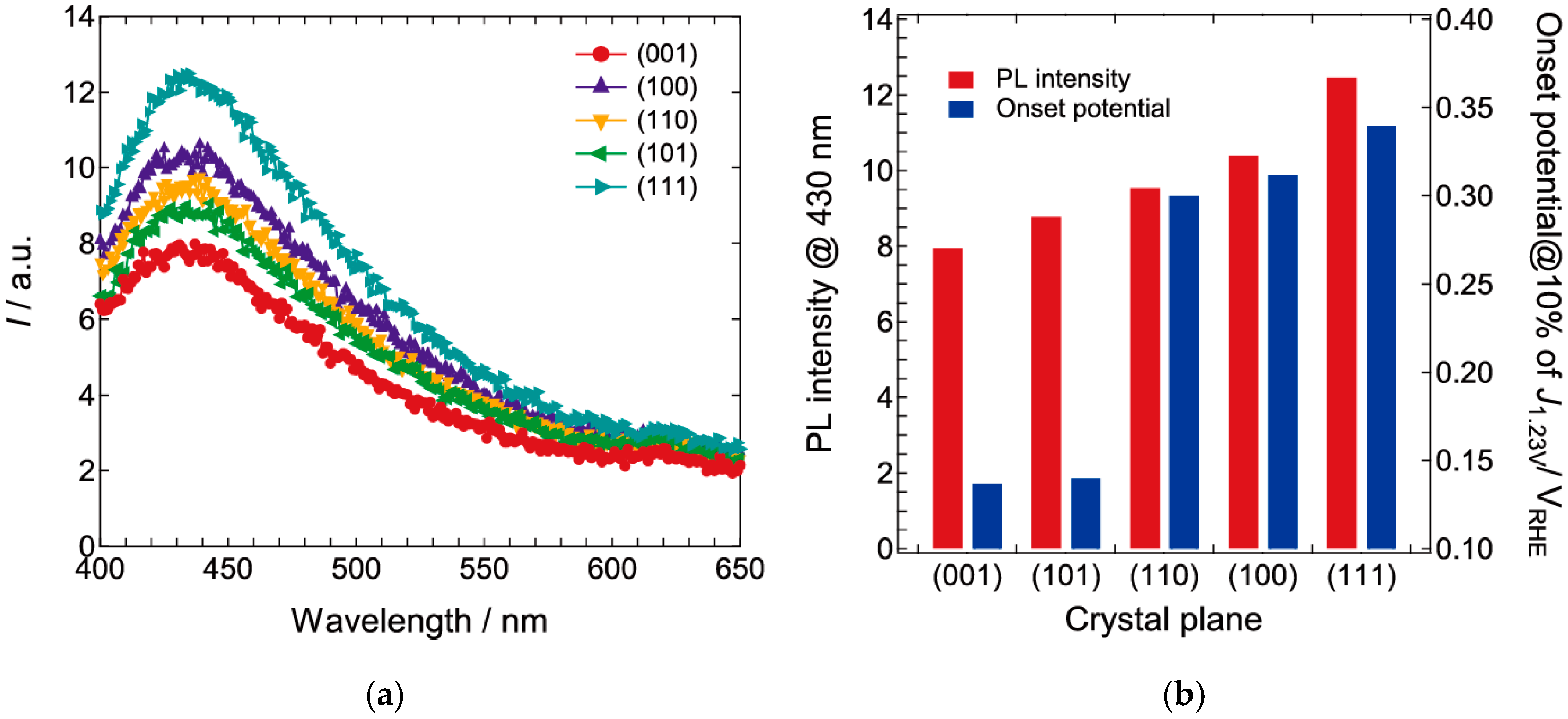
2.2. Photoelectrochemical and Optical Properties

Linear-sweep voltammetry (LSV) in aqueous 1 M KOH electrolyte under 1 sun illumination was carried out to evaluate the PEC properties of the TiO2:Nb single-crystal substrates with (001), (100), (110), (101), and (111) surface planes for water splitting (Figure 5a). The TiO2:Nb(001) substrate showed the largest photocurrent density (J) among the investigated substrates. The open-circuit potential (OCP) under 1 sun illumination was 0.08 V vs. a reversible hydrogen electrode (VRHE). The J increased with increasing applied bias voltage and became saturated at 0.47 mA/cm2 at approximately 0.6 VRHE (Figure 5b). Although the TiO2:Nb(001) photoanode was very flat without any modification of the surface structure to increase its active surface area, the photocurrent would have been very high. For example, this photocurrent value of single crystal TiO2:Nb(001) reached around a half of the value reported in the well-organized Nb-doped TiO2 nanotube arrays [28]. This observation suggests that the Nb-doped TiO2 single crystal and the heterostructure with the very thin rutile TiO2(001) top layer functioned well for PEC water oxidation. The ηmax for this very flat TiO2(001)/TiO2:Nb(001) photoanode was 0.3% at 0.47 VRHE. The PEC performance of the TiO2:Nb substrates was strongly dependent on the crystal planes of the surface. The TiO2:Nb(100) and (110) substrates showed a 20–25% smaller maximum J and 0.10–0.13 VRHE higher OCP than those of TiO2:Nb(001). The TiO2:Nb(101) exhibited a similar OCP value as the TiO2:Nb(001); however, the maximum J remained 75% of that of the TiO2:Nb(001). Among the photoresponses of the investigated substrates, the photoresponse of the TiO2:Nb(111) substrate, in particular, differed from that of the TiO2:Nb(001) substrate. Although the photocurrent started to increase very gradually from 0.08 VRHE, it was not saturated by 1.5 VRHE. The ηmax for TiO2:Nb(111) decreased to 0.05% because of a lack of a steep rise in the photocurrent.
The variations in the PEC properties of the crystal faces in the TiO2:Nb single-crystal photoanodes were likely caused by (1) surface absorption of water molecules, (2) surface recombination of photoexcited electron–hole pairs, and (3) electron transfer at the heterojunction interfaces between the thin semiconducting TiO2 layer and the metal TiO2:Nb base crystal. The surface absorption ability of water molecules in rutile-structured TiO2 crystals has been discussed from the viewpoint of the atomic configurations of Ti and O at the surface. For the (001) direction of TiO2 crystals, the oxygen ions are aligned densely (Figure 1); in addition, the four-fold-coordinated Ti atoms at the (001) plane surface, which are surrounded by bridging oxygen atoms, were evaluated by first-principle calculations to be displaced inside the lattice [29]. As a result of the formation of a high charge density induced by the bridging oxygen ion layer at the top surface, the PEC water oxidation reaction could be enhanced [30,31,32,33]. At the (100) and (110) planes of a TiO2 crystal, the density of Ti ions is relatively higher than at the (001), (101), and (111) planes. The nearest-neighbor Ti–Ti distances for the (100), (110), (001), (101), and (111) planes are 0.296 nm, 0.296 nm, 0.459 nm, 0.357 nm, and 0.546 nm, respectively [22]. The low-coordinate Ti ions at the top surface tend to be electron trapping sites that are unfavorable for the oxidation reaction. Therefore, the (100) and (110) planes of TiO2:Nb substrates could show higher OCP values than the other crystallographic planes. Thus, we considered that the variation of the PEC properties at the TiO2/TiO2:Nb heterojunction would be strongly dependent on the surface affinity of each crystallographic plane for the water molecules. On the basis of this factor, the strange behavior of the LSV curve corresponding to the (111) plane can be also explained. The (111) plane of TiO2 exhibits a relatively low density of Ti ions and is mainly covered by oxygen ions. Therefore, a high electron density would be favorable for the oxidation reaction, resulting in a higher OCP value. However, the (111) surface only has the five-fold-coordinated Ti atoms that do not elaborate the bridging oxygen atoms at the surface; this surface exhibits low adsorption ability for the water molecules. Consequently, the adsorption of water molecules as the rate-limiting reaction would cause a gradual increase of the photocurrent for the applied bias voltage.
Thus, we concluded that the (001) plane of TiO2:Nb crystals was very effective on the PEC oxidation reaction for the water splitting, and the oxidized TiO2 layer on the TiO2:Nb(001) produced the large photocurrent regardless of the very thin thickness. The enhancement of photocurrent would have been strongly related to the surface absorption ability associated with the crystallographic features. On the contrary, the (111) plane of TiO2:Nb, in addition to its poor PEC performance, had difficulty utilizing the surface for the PEC reaction. As shown in Figure 5, the PEC behavior of the TiO2:Nb(111) surface varied greatly during the measurements. In the second run of the LSV measurement, the photocurrent growth behavior already differed from the first run. After the PEC reaction at 1.5 VRHE for 1 h (aged sample), the LSV curve showed a clear saturation at approximately 0.8 VRHE.
Figure 6 shows the field-emission scanning electron microscopy (FESEM) images for the surface morphology of TiO2:Nb(001) and (111) substrates before and after the PEC reaction. The top-surface morphology of both fresh substrates was very flat, without any nanostructuring. However, the surface of TiO2:Nb(111) after the PEC reaction clearly showed a nanoflake array structure as a result of photo-etching. Although a large etching structure was not observed on the TiO2:Nb(001) after the PEC reaction, the surface exhibited a slight granular modulation. For the TiO2 crystals, the top surface can be photo-etched along the <001> direction to make (100) etched pit walls and a (001) basal plane [34,35], and the etching rate under acidic electrolyte conditions is much higher than that under the alkaline condition [36]. In the present study, we carried out the PEC measurements in a strongly alkaline electrolyte (1 M KOH). Nevertheless, strong etching was observed on the TiO2:Nb(111) surface. This etching could be due to the low density of Ti and O ions at the top surface, where only basal planes of isolated pyramidal TiO5 appeared. Therefore, the alkaline (acidic) medium can easily attack the isolated Ti ions at the surface, enabling the penetration of etchant into the crystals. For the other crystal planes, we confirmed that very deep etching as the (111) plane was not observed (Figure S1).
We next evaluated the surface plane dependence of the PEC property for the TiO2:Nb single-crystal substrates on the basis of their optical properties. Figure 7a shows the optical absorption spectrum for each substrate. All of the substrates exhibited large optical absorption of the incident light with wavelengths ranging from the UV to the visible region (300–650 nm). Whereas the absorption of TiO2:Nb(001) was slightly larger (ca. 2–3%) than the absorptions of the other crystal planes over the whole spectral range, the spectral shapes were very similar: The absorption was 70–74% in the visible range (450–650 nm) and decreased to 54–58% with decreasing wavelength. We carried out photon-to-current conversion efficiency (IPCE) measurements at 1.5 VRHE for evaluating the optical absorption effect on the PEC reaction (Figure 7b). The IPCE spectra of the TiO2:Nb substrates at 1.5 VRHE showed 2.4–2.9% absorption at 300 nm that decreased to 0.1% at approximately 410 nm. With increasing wavelength, the IPCE spectra showed a very weak absorption maximum of approximately 0.2% at 505 nm that decreased at wavelengths longer than 580 nm. At the weak maximum (505 nm), the IPCE values for all of the substrates with different crystal planes were very similar to each other. On the contrary, IPCE spectral changes were clearly observed in the UV range rather than in the visible range, whereas the TiO2:Nb exhibited large absorption of visible light by the Nb doped into the TiO2 lattice. The TiO2:Nb(001) exhibited the highest value among them, and the IPCE at 300 nm reached 2.9%. The J variation calculated by the integral of photocurrent collected from the IPCE measurements in the range of 300–700 nm (Table 1 and Figure S2) were almost consistent with the observed J (Figure 5a), while the calculated one for the (111) plane was relatively higher than the observed value.
The aforementioned results indicate that the PEC property was not directly enhanced by the large absorption of visible light by the Nb-doped TiO2 crystals. Enhancement of the PEC property was also observed in the hydrogenated and cation/anion-doped TiO2, especially at the UV range, though the samples also exhibited large optical absorption for visible light [37]. Wang et al. explained this behavior in hydrogenated TiO2 as follows [38]: The hydrogenation of TiO2 increases the electron donor density, resulting in the Fermi level shifting to the conduction band of TiO2. This approach promotes charge separation and transport of photoexcited electron–hole pairs, leading to enhancement of the PEC reaction. The electronic transition between the vacancy level and the delocalized conduction band does not show a substantial contribution to the PEC reaction because of the weak coupling of localized/delocalized energy states. Therefore, the electron–hole pairs photoexcited by the higher photon energy (UV range) associated with the major optical absorption band of TiO2 are considered to mainly contribute to the PEC reaction, which should be enhanced by the electronically-activated transport property derived from the doping/defects in the TiO2 lattice. Our results were also supported by this mechanism. In our case, there are two possible explanations for the excitation and transport process: (1) The stimulation of photoexcited charge separation and transport at the heterointerface between the very thin TiO2 layer and the TiO2:Nb base crystal may enhance the PEC property; and (2) the enhancement of charge separation and transport by doping mainly occurs at the interface between the TiO2/TiO2:Nb and electrolyte.
The charge recombination inhibition scenario would actually work effectively in the TiO2/TiO2:Nb system, although the extent of both contributions is not easy to distinguish because of the ultra-thinness of the TiO2 layer on the base crystal. Figure 8a shows the photoluminescence (PL) spectra for TiO2:Nb single-crystal substrates. The photoluminescence (PL) intensity is generally correlated with the recombination of photoexcited electron–hole pairs, and the intensity variation of TiO2:Nb substrates was strongly related to the photocurrent response behavior. The exact onset potential of the TiO2:Nb(111) was difficult to evaluate correctly because of the very gradual increase of its photocurrent. Therefore, we evaluated the onset potential as a bias voltage at 10% increase from the dark current for the photocurrent at 1.23 VRHE. The PL intensity for each substrate was linked to the onset potential value. This result means the cathodic shift of the photocurrent rise behavior was obviously associated with the inhibition of photoexcited recombination, which was dependent on the crystal surface planes (Figure 8b).

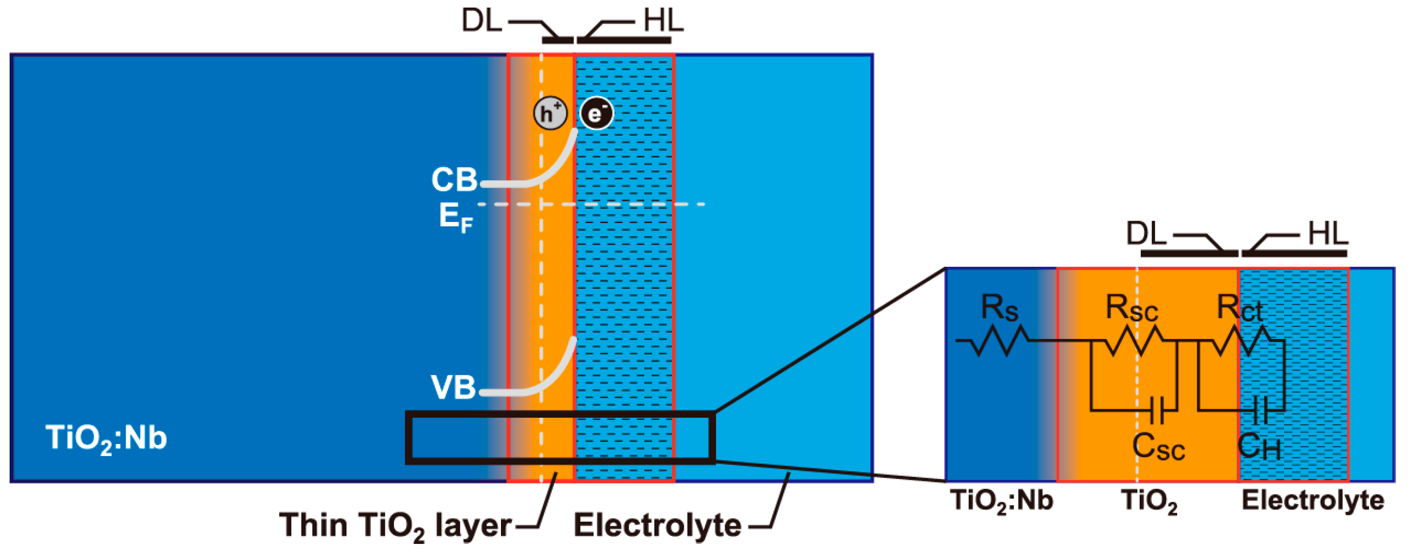
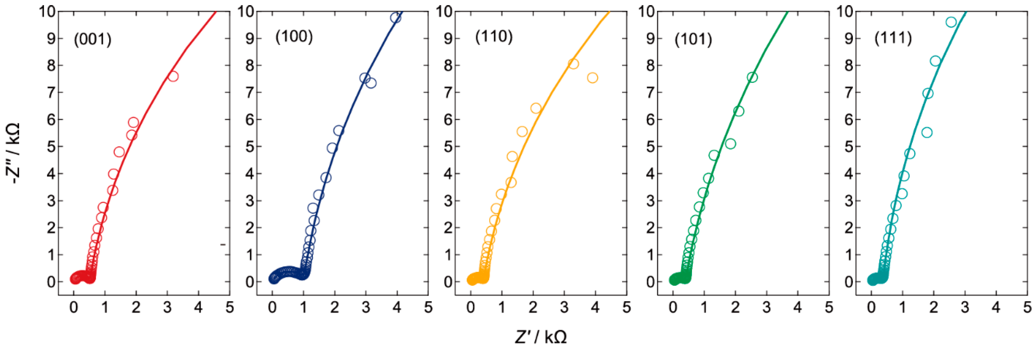
2.3. Electrical Impedance Spectral Analysis of the Transport Property

We carried out electrical impedance spectroscopy (EIS) for the TiO2:Nb single-crystal substrates to evaluate the surface plane dependence of their reaction and transport kinetics. The electrical analog for the electrolyte, TiO2 thin layer, and the TiO2:Nb base crystal is shown in Figure 9. The surface TiO2 thin layer is semiconducting, and it forms an interface with the electrolyte. Therefore, the electrical circuit can be expressed by a series resistance (Rs) and two RC elements for the semiconducting layer (Rsc and space charge capacitance, Csc) and the semiconducting layer and electrolyte interface (Rct and Helmholtz capacitance, CH). For the capacitances of this model, we employed a constant phase element (CPE).
The EIS measurements were carried out for the TiO2:Nb substrates under dark conditions in a three-electrode setup at 1.5 VRHE (Figure 10). Two semicircles were observed in the Nyquist diagrams of both samples, corresponding to the RC elements for the semiconductor layer and the interface between the semiconductor layer and the electrolyte. The fitted parameters based on the equivalent electrical circuit, as shown in Figure 9, are listed in Table 2. Although the resistance value Rs for the base crystal and the parameters associated with the charge transfer phenomena at the interface between the semiconductor layer and the electrolyte (Rct and CH) appeared to not be directly linked to the PEC property, a correlation between the PEC property and the parameters for the depletion layer, Rsc, and Csc was found. The Csc of the (001) plane of TiO2:Nb was especially lower than the others, indicating the efficient reaction of minority carriers in the depletion layer. This efficient reaction could be related to the structural features of the (001) plane. The Ti ions along to the <001> direction are connected via bridging oxygens, whereas the Ti ions link in an oblique direction in the other crystal planes. The structural advantage for transport along the <001> direction can stimulate carrier transport.
We also evaluated the other crystal planes from the EIS results. In the (100) plane of TiO2:Nb, the transient transport property presumed by the Csc was relatively better than that in the (110) and (101) planes; however, the bulk resistance Rsc was more than twice that of the (110) and (101) planes. In the (111) plane, the Csc was very high compared with the other values, which would cause slow dynamics of charge transfer. On the basis of these results, the EIS parameters did not play a critical role in the PEC property. However, only the (001) plane showed a clear advantage (very low Csc) and did not have a large disadvantage with respect to photocarrier transport. The heteroepitaxial relationship between the TiO2 layer and the TiO2:Nb(001) was also considered to positively affect carrier transport. In addition to the aforementioned (001) surface structural features that favor the water oxidation reaction, the transportation enhancement in the depletion layer near the heterointerface between the TiO2 thin layer and the base crystal was an important origin of the good PEC reaction on the TiO2:Nb(001) substrate.

3. Materials and Methods

3.1. Materials

The 0.43 at% Nb-doped TiO2 and pure TiO2 crystals used in the experiments were commercial rutile-structured single-crystal substrates with five different surface orientations ((001), (100), (110), (101), and (111) for the Nb-doped TiO2 and (001) for the TiO2) (SHINKOSHA). The reference TiO2:Nb2O5 (0.43 at% Nb) polycrystalline powder composite was synthesized by the solid-state reaction of TiO2 (rutile) and Nb2O5 with 99.99% purities (rare metallic). Starting reagents were ground thoroughly, pressed into pellets, and then heated at 800 °C for 12 h in air.

3.2. Sample Characterization

AFM images were recorded with a Nanoscope IIIa (Digital Instruments, NY, USA) using a silicon cantilever in tapping mode. XPS measurements were performed using a PHI ESCA model 5800 system (ULVAC-PHI, Inc., Kanagawa, Japan) with monochromatic Al Kα excitation (1486.6 eV) at 100 W with a pass energy of 23.50 eV and a step size of 0.1 eV. The intensity analyses were carried out using Ti 2p3/2 peaks as a reference. The signals were deconvoluted with Gaussian peak shapes. The surface morphology was determined by FESEM; Hitachi SU9000 (Tokyo, Japan). The optical absorbance spectra were recorded using a UV-visible spectrophotometer (UV-3150, Shimadzu, Kyoto, Japan). The PL spectra were evaluated with a C9920-02 spectrometer (Hamamatsu Photonics, Shizuoka, Japan) equipped with an Xe lamp, a monochromator, a back-illuminated multichannel charge-coupled device photodetector, and an integrating sphere.

3.3. PEC Performance Evaluation

Under 100 mW/cm2 AM1.5 simulated sunlight (1 sun) from a 150 W Xe lamp, LSV for solar water-splitting photocurrent measurements was performed in 1.0 M KOH (pH = 13.6) at 0.0–1.5 V vs. a reversible hydrogen electrode (VRHE) in a three-electrode electrochemical cell equipped with a quartz glass window. An Ag/AgCl reference electrode in saturated KCl solution and a Pt wire counter electrode were used, and the scan rate was 5 mV/s. The measured potential vs. Ag/AgCl (VAg/AgCl) in the three-electrode system was converted to the VRHE according to a following equation: VRHE = VAg/AgCl + 0.059 pH + V0Ag/AgCl, where V0Ag/AgCl = 0.1976 at 25 °C. The STH efficiency (η) of the photoanodes was measured using a two-electrode configuration cell with a Pt wire as the counter electrode. The following equation was used for estimating STH values: η = J (1.23 − ECE)/IAM1.5, where J is the photocurrent density (mA/cm2), ECE is the applied bias voltage vs. the counter electrode, and IAM1.5 is the irradiance of AM1.5 simulated sunlight at 100 mW/cm2. The IPCE was evaluated using the three-electrode setup with the equation IPCE = 1240 J/λI, where λ is the incident-light wavelength (nm) and I is the intensity of the light source at each wavelength (mW/cm2). The bias voltage was 0.55 VRHE. The monochromatic light was generated using an Xe lamp with optical narrow-band filters. EIS measurements were performed on a PGSTAT302N potentiostat equipped with an impedance analyzer FRA32M (Metrohm Autolab, Herisau, Switzerland). The frequency range was from 0.01 Hz to 100 kHz, and the modulation signal was 10 mV. All measurements were conducted at 1.5 VRHE under 1 sun illumination.

4. Conclusions

We showed the crystal-plane dependence of PEC water-splitting property for the rutile TiO2:Nb single-crystal substrates, and that the (001) crystal plane was the most promising surface for obtaining the good photocurrent. We revealed that the doped Nb ions were segregated from the top surface, and that the TiO2 thin layer was formed at the surface of crystal, resulting in the formation of a heterointerface between the TiO2 and TiO2:Nb. The enhancement of PEC property in the TiO2:Nb(001) single-crystal substrate was originated from the favorable atomic configurations for the water molecule absorption and the facilitation of transportation of photoexcited electron/hole pairs in the depletion layer formed around the heterointerface of TiO2 thin layer with the base crystal.

Supplementary Materials

The following are available online at https://www.mdpi.com/2073-4344/9/9/725/s1, Figure S1: The surface morphology for the (100)-, (110)- and (101)-planes of TiO2:Nb substrates after the PEC reaction at 1.5 VRHE for 1 h in 1 M KOH electrolyte. The white scale bars represent 500 nm., Figure S2: The spectra for 100 mW·cm-2 AM1.5G (1 SUN) and simulated solar light used for the IPCE measurements.

Author Contributions

T.N. (Tomohiko Nakajima) conducted most of the experiments and analyses and wrote the manuscript. T.N. (Takako Nakamura) carried out the XPS analysis. All authors discussed the experimental results and interpretation.

Funding

This work was partly supported by a Grant-in-Aid for Young Scientists (B) No. 25820338 from the Japan Society for the Promotion of Science.

Acknowledgments

The authors thank N. Fukuda for the technical help.

Conflicts of Interest

The authors declare no conflicts of interest.

References

  1. Alexander, B.D.; Kulesza, P.J.; Rutkowska, I.; Solarska, R.; Augustynski, J. Metal oxide photoanodes for solar hydrogen production. J. Mater. Chem. 2008, 18, 2298–2303. [Google Scholar] [CrossRef]
  2. Nowotny, J.; Bak, T.; Nowotny, M.K.; Sheppard, L.R. Titanium dioxide for solar-hydrogen I. Functional properties. Int. J. Hydrogen Energy 2007, 32, 2609–2629. [Google Scholar] [CrossRef]
  3. Kronawitter, C.X.; Vayssieres, L.; Shen, S.; Guo, L.; Wheeler, D.A.; Zhang, J.Z.; Antoun, B.R.; Mao, S.S. A perspective on solar-driven water splitting with all-oxide hetero-nanostructures. Energy Environ. Sci. 2011, 4, 3889–3899. [Google Scholar] [CrossRef]
  4. Osterloh, F.E. Inorganic nanostructures for photoelectrochemical and photocatalytic water splitting. Chem. Soc. Rev. 2013, 42, 2294–2320. [Google Scholar] [CrossRef] [PubMed]
  5. Nakajima, T.; Hagino, A.; Nakamura, T.; Tsuchiya, T.; Sayama, K. WO3 nanosponge photoanodes with high applied bias photon-to-current efficiency for solar hydrogen and peroxydisulfate production. J. Mater. Chem. A 2016, 4, 17809–17818. [Google Scholar] [CrossRef]
  6. Dang, H.X.; Hahn, N.T.; Park, H.S.; Bard, A.J.; Mullins, C.B. Nanostructured Ta3N5 films as visible-light active photoanodes for water oxidation. J. Phys. Chem. C 2012, 116, 19225–19232. [Google Scholar] [CrossRef]
  7. Nakajima, T.; Lee, C.-Y.; Yang, Y.; Schmuki, P. N-Doped lepidocrocite nanotubular arrays: Hydrothermal formation from anodic TiO2 nanotubes and enhanced visible light photoresponse. J. Mater. Chem. A 2013, 1, 1860–1866. [Google Scholar] [CrossRef]
  8. Wang, Z.; Yang, C.; Lin, T.; Yin, H.; Chen, P.; Wan, D.; Xu, F.; Huang, F.; Lin, J.; Xie, X.; et al. Visible-light photocatalytic, solar thermal and photoelectrochemical properties of aluminium-reduced black titania. Energy Environ. Sci. 2013, 6, 3007–3014. [Google Scholar] [CrossRef]
  9. Yi, Z.; Ye, J.; Kikugawa, N.; Kako, T.; Ouyang, S.; Stuart-Williams, H.; Yang, H.; Cao, J.; Luo, W.; Li, Z.; et al. An orthophosphate semiconductor with photooxidation properties under visible-light irradiation. Nat. Mater. 2010, 9, 559–564. [Google Scholar] [CrossRef]
  10. Pan, X.; Yang, M.-Q.; Fu, X.; Zhang, N.; Xu, Y.-J. Defective TiO2 with oxygen vacancies: Synthesis, properties and photocatalytic applications. Nanoscale 2013, 5, 3601–3614. [Google Scholar] [CrossRef]
  11. Pinaud, B.A.; Vesborg, P.C.K.; Jaramillo, T.F. Effect of film morphology and thickness on charge transport in Ta3N5/Ta photoanodes for solar water splitting. J. Phys. Chem. C 2012, 116, 15918–15924. [Google Scholar] [CrossRef]
  12. Seki, M.; Yamahara, H.; Tabata, H. Enhanced photocurrent in Rh-substituted α-Fe2O3 thin films grown by pulsed laser deposition. Appl. Phys. Express 2012, 5, 115801-1–115801-3. [Google Scholar] [CrossRef]
  13. Nakajima, T.; Nakamura, T.; Tsuchiya, T. The significant effect of heterojunction quality on photoelectrochemical water splitting in bilayer photoelectrodes: RbxWO3 thin films on RbLaNb2O7 layers. Phys. Chem. Chem. Phys. 2014, 16, 26901–26908. [Google Scholar] [CrossRef] [PubMed]
  14. Mu, L.; Zhao, Y.; Li, A.; Wang, S.; Wang, Z.; Yang, J.; Wang, Y.; Liu, T.; Chen, R.; Zhu, J.; et al. Enhancing charge separation on high symmetry SrTiO3 exposed with anisotropic facets for photocatalytic water splitting. Energy Environ. Sci. 2016, 9, 2463–2469. [Google Scholar] [CrossRef]
  15. Li, W.; Bai, Y.; Liu, W.; Liu, C.; Yang, Z.; Feng, X.; Lu, X.; Chan, K.-Y. Single-crystalline and reactive facets exposed anatase TiO2 nanofibers with enhanced photocatalytic properties. J. Mater. Chem. 2011, 21, 6718–6724. [Google Scholar] [CrossRef]
  16. Ye, L.; Mao, J.; Liu, J.; Jiang, Z.; Peng, T.; Zan, L. Synthesis of anatase TiO2 nanocrystals with {101}, {001} or {010} single facets of 90% level exposure and liquid phase photocatalytic reduction and oxidation activity orders. J. Mater. Chem. A 2013, 1, 10532–10537. [Google Scholar] [CrossRef]
  17. Ballestas-Barrientos, A.; Li, X.; Yick, S.; Masters, A.F.; Maschmeyer, T. Optimised heterojunctions between [100]-oriented rutile TiO2 arrays and {001} faceted anatase nanodomains for enhanced photoelectrochemical activity. Sustain. Energy Fuels 2018, 2, 1463–1473. [Google Scholar] [CrossRef]
  18. Hitosugi, T.; Ueda, A.; Nakao, S.; Yamada, N.; Furubayashi, Y.; Hirose, Y.; Shimada, T.; Hasegawa, T. Fabrication of highly conductive Ti1−xNbxO2 polycrystalline films on glass substrates via crystallization of amorphous phase grown by pulsed laser deposition. Appl. Phys. Lett. 2007, 90, 212106-1–212106-3. [Google Scholar] [CrossRef]
  19. Tucker, R.T.; Beckers, N.A.; Fleischauer, M.D.; Brett, M.J. Electron beam deposited Nb-doped TiO2 toward nanostructured transparent conductive thin films. Thin Solid Films 2012, 525, 28–34. [Google Scholar] [CrossRef]
  20. Trenczek-Zając, A.; Radecka, M.; Rekas, M. Photoelectrochemical properties of Nb-doped titanium dioxide. Physica B Condens. Matter 2007, 399, 55–59. [Google Scholar] [CrossRef]
  21. Yang, M.; Jha, H.; Liu, N.; Schmuki, P. Increased photocurrent response in Nb-doped TiO2 nanotubes. J. Mater. Chem. 2011, 21, 15205–15208. [Google Scholar] [CrossRef]
  22. Baur, W.H.; Khan, A.A. Rutile-type compounds. VI. SiO2, GeO2 and a comparison with other rutile-type structures. Acta Crystallogr. B 1971, 27, 2133–2139. [Google Scholar] [CrossRef]
  23. Philippin, G.; Delhalle, J.; Mekhalif, Z. Comparative study of the monolayers of CH3–(CH2)n–SiCl3 and CH3–(CH2)n–PO(OH)2, n = 4 and 13, adsorbed on polycrystalline titanium substrates. Appl. Surf. Sci. 2003, 212–213, 530–536. [Google Scholar] [CrossRef]
  24. Kačiulis, S.; Mattogno, G.; Napoli, A.; Bemporad, E.; Ferrari, F.; Montenero, A.; Gnappi, G. Surface analysis of biocompatible coatings on titanium. J. Electron Spectrosc. 1998, 95, 61–69. [Google Scholar] [CrossRef]
  25. Nakajima, T.; Nakamura, T.; Shinoda, K.; Tsuchiya, T. Rapid formation of black titania photoanodes: Pulsed laser-induced oxygen release and enhanced solar water splitting efficiency. J. Mater. Chem. A 2014, 2, 6762–6771. [Google Scholar] [CrossRef]
  26. Krishna, V.; Bai, W.; Han, Z.; Yano, A.; Thakur, A.; Georgieva, A.; Tolley, K.; Navarro, J.; Koopman, B.; Moudgil, B. Contaminant-activated visible light photocatalysis. Sci. Rep. 2018, 8, 1894-1–1894-11. [Google Scholar] [CrossRef]
  27. Idriss, H. Surface reactions of uranium oxide powder, thin films and single crystals. Surf. Sci. Rep. 2010, 65, 67–109. [Google Scholar] [CrossRef]
  28. Das, C.; Roy, P.; Yang, M.; Jha, H.; Schmuki, P. Nb doped TiO2 nanotubes for enhanced photoelectrochemical water-splitting 2011, 3, 3094–3096. Nanoscale 2011, 3, 3094–3096. [Google Scholar] [CrossRef]
  29. Ramamoorthy, M.; Vanderbilt, D.; King-Smith, R.D. First-principle calculations of the energetics of stoichiometric TiO2 surfaces. Phys. Rev. B 1994, 49, 16721–16727. [Google Scholar] [CrossRef]
  30. Lowekamp, J.B.; Rohrer, G.S.; Hotsenpiller, P.A.M.; Bolt, J.D.; Farneth, W.E. Anisotropic photochemical reactivity of bulk TiO2 crystals. J. Phys. Chem. B 1998, 102, 7323–7327. [Google Scholar] [CrossRef]
  31. Ohno, T.; Sarukawa, K.; Matsumura, M. Crystal faces of rutile and anatase TiO2 particles and their roles in photocatalytic reactions. New J. Chem. 2002, 26, 1167–1170. [Google Scholar]
  32. Haisch, C.; Günnemann, C.; Melchers, S.; Fleisch, M.; Schneider, J.; Emeline, A.V.; Bahnemann, D.W. Irreversible surface changes upon n-type doping—A photoelectrochemical study on rutile single crystals. Electrochim. Acta 2018, 280, 278–289. [Google Scholar]
  33. Fujishima, A.; Zhang, X.; Tryk, D.A. TiO2 photocatalysis and related surface phenomena. Surf. Sci. Rep. 2008, 63, 515–582. [Google Scholar] [CrossRef]
  34. Harris, L.A.; Wilson, R.H. Aging effects in single crystal reduced rutile anodes. J. Electrochem. Soc. 1976, 123, 1010–1015. [Google Scholar] [CrossRef]
  35. Tsujiko, A.; Kisumi, T.; Magari, Y.; Murakoshi, K.; Nakato, Y. Selective formation of nanoholes with (100)-face walls by photoetching of n-TiO2 (rutile) electrodes, accompanied by increases in water-oxidation photocurrent. J. Phys. Chem. B 2000, 104, 4873–4879. [Google Scholar] [CrossRef]
  36. Imanishi, A.; Okamura, T.; Ohashi, N.; Nakamura, R.; Nakato, Y. Mechanism of water photooxidation reaction at atomically flat TiO2 (rutile) (110) and (100) surfaces: Dependence on solution pH. J. Am. Chem. Soc. 2007, 129, 11569–11578. [Google Scholar] [CrossRef]
  37. Hu, Y.H. A highly efficient photocatalyst—hydrogenated black TiO2 for the photocatalytic splitting of water. Angew. Chem. Int. Ed. 2012, 51, 12410–12412. [Google Scholar] [CrossRef]
  38. Wang, G.; Wang, H.; Ling, Y.; Tang, Y.; Yang, X.; Fitzmorris, R.C.; Wang, C.; Zhang, J.Z.; Li, Y. Hydrogen-treated TiO2 nanowire arrays for photoelectrochemical water splitting. Nano Lett. 2011, 11, 3026–3033. [Google Scholar] [CrossRef]
Figure 1. Schematic crystal structures for the (001), (100), (110), (101), and (111) planes of TiO2:Nb. The light-blue and red spheres represent titanium and oxygen atoms, respectively. Some of the titanium atoms have been substituted by niobium atoms (0.43 at%). The gray planes and dotted ovals represent the crystal surface and bridging oxygen atoms, respectively.
Catalysts 09 00725 g001
Figure 2. (a) AFM images and (b) surface roughness (Ra) values for the TiO2:Nb single-crystal substrates.
Catalysts 09 00725 g002
Figure 3. XPS spectra for (a) Ti 2p, (b) Nb 3d, and (c) O 1s core levels in the TiO2:Nb (TiO2) single-crystal substrates and TiO2:Nb2O5 polycrystalline powder.
Catalysts 09 00725 g003
Figure 4. (a) Relative peak intensity ratio in the XPS spectra for Nb 3d3/2 and Ti 2p1/2 and the calculated Nb content (at%). (b) Relative peak intensity ratio in the XPS spectra for Ti–OH and Ti–O at the O 1s in the TiO2:Nb (TiO2) single-crystal substrates and TiO2:Nb2O5 polycrystalline powder.
Catalysts 09 00725 g004
Figure 5. (a) The LSV curves for the TiO2:Nb(001), (100), (110), (101), and (111) single-crystal substrates. The “1st” and “2nd” simply represent the frequency of LSV measurement for the fresh substrate. The data which do not show the annotation mean measurements for the fresh substrates. The “aged” represent the sample after the PEC reaction at 1.5 VRHE for 30 min. (b) The surface plane dependence of TiO2:Nb substrates on J at 1.23 VRHE (J1.23V), OCP, ηmax, and effective bias potential for the ηmax (EOP).
Catalysts 09 00725 g005
Figure 6. The surface morphology for the (a) (001)- and (b) (111)-planes of TiO2:Nb substrates before and after the PEC reaction at 1.5 VRHE for 1 h in 1 M KOH electrolyte. The white scale bars represent 500 nm.
Catalysts 09 00725 g006
Figure 7. (a) Optical absorption and (b) IPCE spectra for the TiO2:Nb(001), (100), (110), (101), and (111) single-crystal substrates. The IPCE data were recorded at 1.5 VRHE in 1 M KOH electrolyte under monochromatic light illumination.
Catalysts 09 00725 g007
Figure 8. (a) PL spectra for the TiO2:Nb substrates excited at 350 nm. (b) The PL intensity at 430 nm and onset potential defined as the bias voltage at 10% of the photocurrent at 1.23 VRHE for each substrate.
Catalysts 09 00725 g008
Figure 9. Energy diagram and electrical circuit analog for the TiO2/TiO2:Nb. The CB, VB, EF, DL and HL represent the conduction band, valance band, Fermi energy, depletion layer and Helmholtz layer, respectively.
Catalysts 09 00725 g009
Figure 10. The Nyquist diagrams of TiO2:Nb single-crystal substrates with the (001), (100), (110), (101), and (111) crystal-plane surface measured at 1.5 VRHE under 1 sun illumination.
Catalysts 09 00725 g010
Table 1. Observed J at 0.55 VRHE (J0.55V) and calculated J value from the IPCE spectra.
Lattice PlaneJ0.55V/mA/cm2JIPCE/mA/cm2
(001)0.4440.393
(100)0.3140.316
(110)0.3420.345
(101)0.3390.329
(111)0.0570.290
Table 2. Fitted parameters of the Nyquist plots for single-crystal TiO2:Nb photoanodes.
LATTICE PLANERsRscCPEscRct/kΩCPEH
Csc/nFsn−1nCH/μFsn−1n
(001)15.7496.351.90.91442.33.340.918
(100)11.8853.42420.78555.93.810.926
(110)17.2385.73630.80044.04.340.912
(101)16.5377.23550.80260.54.350.908
(111)9.66368.07830.75158.72.840.947

