
Review

Application of Transition Metal Dichalcogenides in Electrocatalytic Hydrogen Evolution Reaction

1
College of Materials Science and Engineering, Changchun University of Technology, Changchun 130051, China
2
Hubei Key Laboratory of Energy Storage and Power Battery, School of Automotive Materials, Hubei University of Automotive Technology, Shiyan 442002, China
*
Authors to whom correspondence should be addressed.
These authors contributed equally to this work.
Catalysts 2026, 16(3), 266; https://doi.org/10.3390/catal16030266
Submission received: 10 February 2026 / Revised: 4 March 2026 / Accepted: 11 March 2026 / Published: 15 March 2026
(This article belongs to the Special Issue Theoretical and Experimental Research on Catalytic Hydrogen Evolution)

Abstract

As a cornerstone of sustainable hydrogen generation, the hydrogen evolution reaction (HER) demands efficient, earth-abundant electrocatalysts to replace costly platinum benchmarks. Two-dimensional transition metal dichalcogenides (2D-TMDs) represent a highly promising class of non-precious materials for this application. This review provides a comprehensive analysis of recent progress in TMD-based HER catalysis. It begins by elucidating the intrinsic structural properties that underpin their catalytic potential, followed by a summary of key synthesis routes and characterization techniques. The central focus is on strategic engineering approaches to optimize TMD performance. Finally, we discuss persisting challenges and propose future research directions aimed at scalable production, advanced operando studies, and the design of bifunctional TMD catalysts for integrated water-splitting systems.

Graphical Abstract

1. Introduction

The continuous surge in global energy demand and excessive consumption of fossil fuels have rendered the energy crisis and environmental pollution critical global challenges that demand urgent solutions [1,2]. Consequently, the development of clean, efficient, and sustainable alternative energy sources has become a core task for both the scientific and industrial communities [1]. Hydrogen energy, as an ideal clean energy carrier with zero carbon emissions and a high energy density of approximately 142 MJ/kg, exhibits tremendous potential in the energy transition [3]. However, efficient hydrogen production technology remains a bottleneck restricting the large-scale application of hydrogen energy. Currently, industrial hydrogen production primarily relies on fossil fuel reforming [1,4]. Alternatively, the electrocatalytic hydrogen evolution reaction (HER) via water electrolysis is recognized as a core technological pathway for future hydrogen production [5]. Nevertheless, traditional electrocatalytic HER catalysts are mainly based on precious metals such as Pt and Pd [6,7]. Although these materials possess excellent catalytic activity and stability, their scarcity and high cost limit the practical application of water electrolysis for hydrogen production [1,2]. Therefore, developing low-cost, high-activity, and long-lifespan non-precious metal HER catalysts has become a key scientific challenge to break through the bottlenecks in hydrogen production technology and advance the clean energy revolution.
Two-dimensional (2D) materials are prominent non-precious metal candidates for electrocatalysis, owing to their high specific surface area, tunable composition, and abundant active sites [3,8]. Their layered structure, held together by weak interlayer van der Waals forces, allows for easy exfoliation into mono- or few-layer nanosheets [6,9]. This process exposes a vast surface area, which is critical for heterogeneous surface catalysis. The electronic structure of these materials can be precisely optimized for electrocatalytic activity through layer control, composition modification, and defect engineering [4,6,10]. Among them, transition metal dichalcogenides (TMDs) offer exceptional tunability due to their mixed metallic and non-metallic character, making them particularly attractive for the HER. In TMDs like MoS2, the catalytically active sites are primarily located at the edges, where the hydrogen adsorption free energy (ΔGH*) approaches that of Pt, while the basal planes are largely inert [4,9,11,12]. Further enhancement of their electron transport and catalytic performance can be achieved through elemental doping, defect engineering, and heterostructure construction, solidifying their status as ideal substitutes for precious metal catalysts [12,13,14,15].
Despite their remarkable advantages, 2D TMDs still have several limitations [1,6,14]. In terms of stability, they are prone to oxidation and dissolution (e.g., the S element dissolves in the form of SO42−) during long-term catalytic processes, which affects their service lifespan [4,16]. Regarding the regulation of active sites, although edge sites and defect sites have been identified as active centers, precise control over their quantity and distribution still requires support from in situ characterization techniques [4,16]. In terms of preparation technology, high-quality nanosheets currently mostly rely on laboratory methods such as chemical vapor deposition (CVD) and liquid-phase exfoliation, which are difficult to scale up to meet industrial demands [9,17]. Current research has shifted from single-component systems toward multi-component, high-entropy, and heterostructure systems [12,15,18]. For example, high-entropy dichalcogenides like (TiVCrNbTa)S2 achieve a metal–insulator transition through the synergistic effect of multiple metal elements [9]; the SnS2/MoS2 heterojunction activates the inert basal plane of MoS2 via interfacial charge transfer, reducing the HER overpotential to 240 mV (at 10 mA cm−2) [9]. Some novel 2D TMD materials with some effective strategies have even achieved activity and stability comparable to commercial Pt/C catalysts in acidic or alkaline electrolytes [4,16,19].
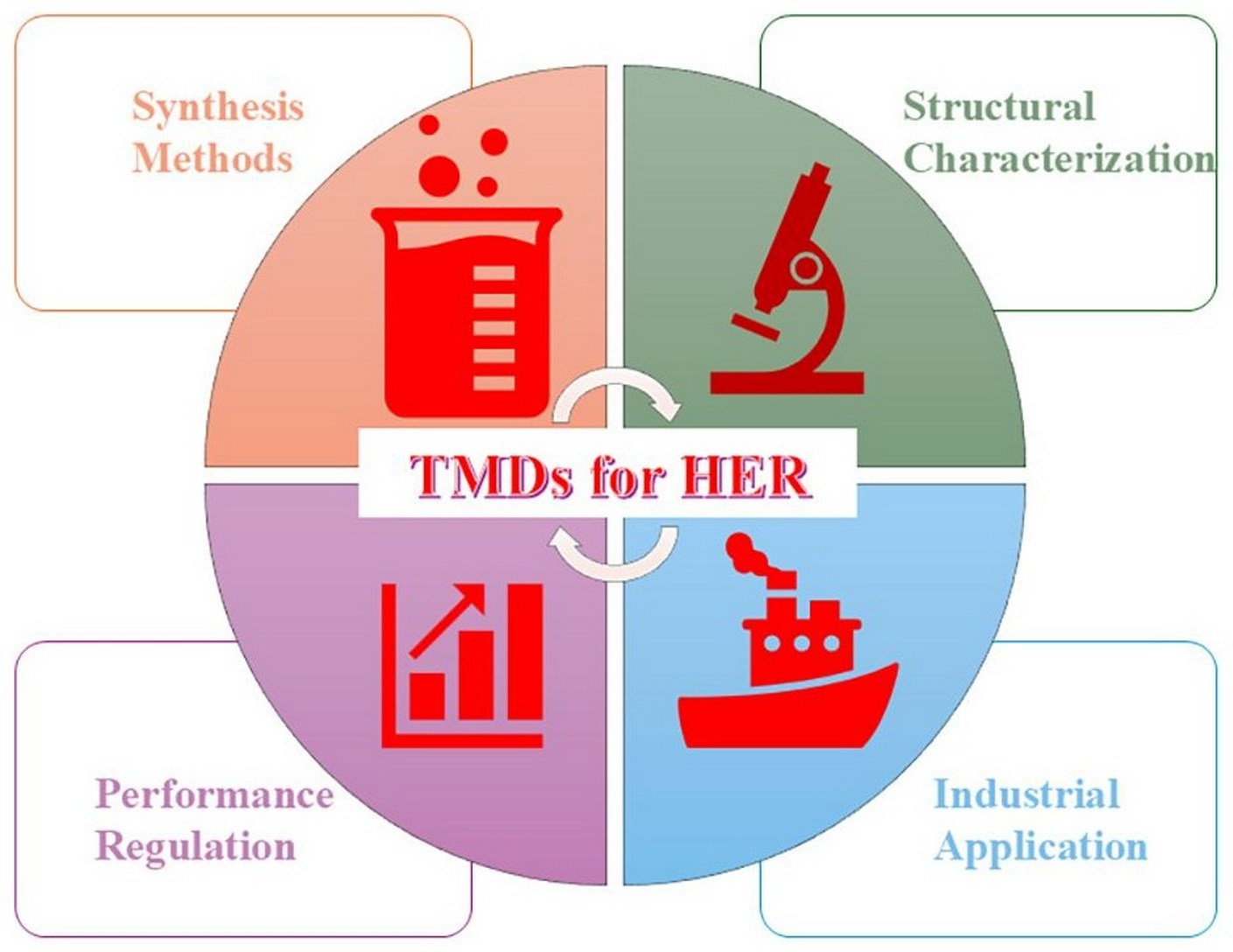
Existing reviews on TMD-based HER catalysts have laid solid foundations for the field. Most studies focus on single modification strategy summarization, such as systematically elaborating on defect engineering (vacancy, edge site regulation) or heterostructure construction (TMDs/graphene, TMDs/metal oxides) and their impact on catalytic activity [4,19]. Some reviews emphasize performance comparison of specific TMDs systems (e.g., MoS2, WS2) in different electrolytes, or focus on synthetic method optimization (CVD, hydrothermal) for large-scale preparation [16,18]. A few reviews touch on multi-component regulation but lack in-depth discussion on the synergistic mechanism of high-entropy TMDs, and rarely integrate “synthesis-method → structural-characterization → performance-regulation → industrial-prospect” into a complete logical chain [19]. Additionally, most reviews pay insufficient attention to the practical application bottlenecks of TMDs (e.g., long-term stability in complex electrolytes, scalability of synthesis) and lack targeted analysis of structure–activity relationships based on in situ characterization and theoretical calculations [4,9].
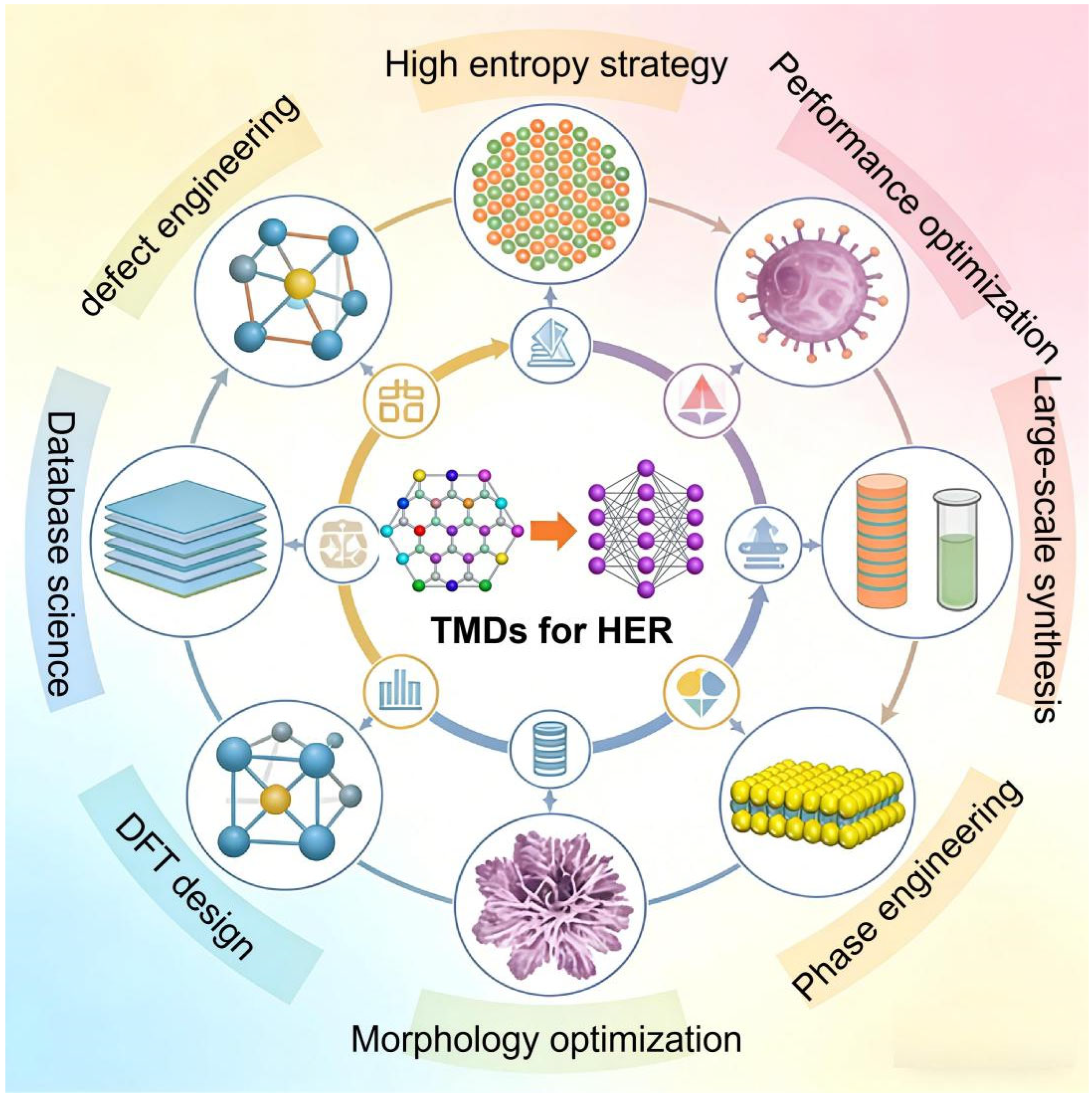
Compared with these existing works, this review has three distinct features: First, systematic integration of multi-scale regulation strategies: we not only cover traditional strategies such as doping, defect engineering, and heterostructure construction but also focus on emerging directions like high-entropy alloying and moiré superlattice regulation, revealing the synergistic mechanism of multi-element and multi-structure in optimizing TMDs performance. Second, deep integration of characterization and theory: we comprehensively summarize key characterization methods (in situ XAS, STEM, AFM) for TMDs, and correlate experimental data with DFT calculations to clarify the origin of active sites and electron transfer pathways, avoiding isolated discussion of performance or structure. Third, practical orientation toward industrial application: we emphasize the scalability of synthetic methods (e.g., ball milling, template-guided synthesis) and analyze the stability of TMDs in complex environments while proposing targeted solutions for current challenges, bridging the gap between laboratory research and industrial application.
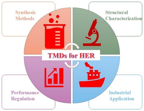
To deepen the understanding of the structure, electronic properties, and catalytic efficacy of 2D TMDs, this review critically examines their application in the HER and outlines future research trajectories (Figure 1). We consolidate a wide array of synthetic and modification strategies, correlating them with the distinct attributes of different TMD materials. Furthermore, we elaborate on the suite of characterization methods essential for evaluating these catalysts. Building on this foundation, the review concludes with a prospective outlook, pinpointing current limitations and proposing strategic directions for the rational design and enhancement of next-generation TMD-based electrocatalysts.

2. TMD Materials Characteristics

2.1. Classification and Structure of TMDs

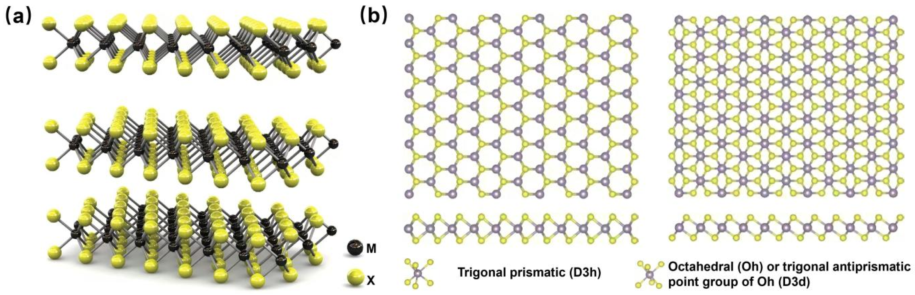
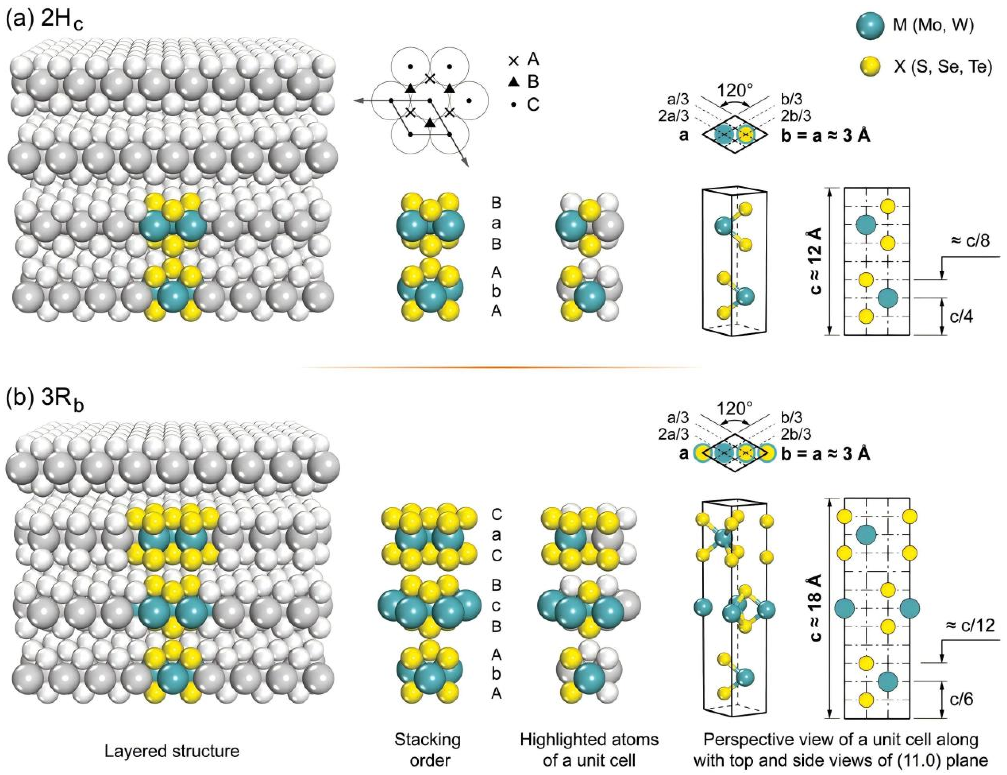
TMDs can be classified by their dimensionality: zero-dimensional (0D), one-dimensional (1D), two-dimensional (2D), and three-dimensional (3D) structures [10]. Among these, low-dimensional TMDs (particularly 0D, 1D, and 2D) have garnered significant interest due to their unique properties, which differ markedly from those of their bulk 3D counterparts [10]. 0D TMD materials refer to structures with all dimensions being in the range of 1~100 nm, which typically consist of transition metals from Group IB to Group IIB and chalcogens, with a composition ratio of M:X ranging from 1:1 to 1:2. Their unique physical and chemical properties make them highly promising for photoluminescence, photocatalysis, and photothermal therapy [10]. 1D TMD nanostructures have great potential in photonics and thermoelectrics applications due to their tunable quantum confinement effects [10]. The chemical formula of 2D TMD can be represented as MX2, where M represents a transition metal spanning from group IVB (Ti, Zr, Hf), group VB (V, Nb, Ta), group VIB (Mo, W), group VIIB (Re) to group VIII (Pd, Pt). X represents a chalcogen (S, Se, Te) [20]. 2D TMD can be classified into nanosheets and nanoribbons according to the external dimensions and internal structure of its nanomaterials [21]. In a 2D TMD structure, atoms within the same layer are chemically bonded, while those between layers interact through weak van der Waals force [10]. Bulk 2D-based materials can be straightforwardly exfoliated into atomically thin layer sheets, including single and/or double layer, owing to the presence of weak van der Waals force between the layers, which can be easily separated with minimum efforts depending on their different physicochemical properties such as density, conductivity, corrosion resistance, melting point, and chemical stability [20]. TMDs have layered structures with two main distinguished polytypes, 2Hc and 3Rb, belonging to the hexagonal crystal family, but different in stacking order. Monolayers of MX2, as the building blocks of bulk MX2 crystal, are identical in both polytypes and consist of an atomic plane of hexagonally packed metal atoms sandwiched between two similar hexagonally packed atomic planes made up of chalcogen atoms. The bonding within the monolayer is covalent, while these three-atomic-thick layers are held together by weak van der Waals forces in the bulk crystal. The most common naturally occurring polytype, 2Hc, also known as 2H-MX2, has the stacking order AbA|BaB where the capital letter “H” indicates the hexagonal crystal lattice and the preceding digit “2” refers to two molecules in the unit cell, as shown in Figure 2a [21]. On the other hand, the 3Rb polytype, also known as 3R-MX2, has the stacking order AbA|BcB|CaC where the capital letter “R” indicates the rhombohedral crystal lattice and digit “3” refers to three molecules per unit cell. Thus, the height of the 3Rb unit cell is about 1.5 times larger than that of the 2Hc, as shown in Figure 2b [21]. In addition, lattice constants increase upon going from sulfides to tellurides in both MoX2 and WX2 crystals. The z-parameter also slightly decreases from sulfides to tellurides indicating a smaller van der Waals gap between the monolayers in the bulk unit cell, or in the other words, thicker monolayer in the series from MS2 to MTe2 with respect to the c lattice constant. This parameter influences the M-X bond length, and recently it has been shown that it is critical to accurately calculate the electronic band structure of MX2 and hybridization between M-d and X-p orbitals. Density and molar mass of TMD are also increased from sulfides to tellurides and are higher for tungsten dichalcogenides relative to their molybdenum counterparts [21].
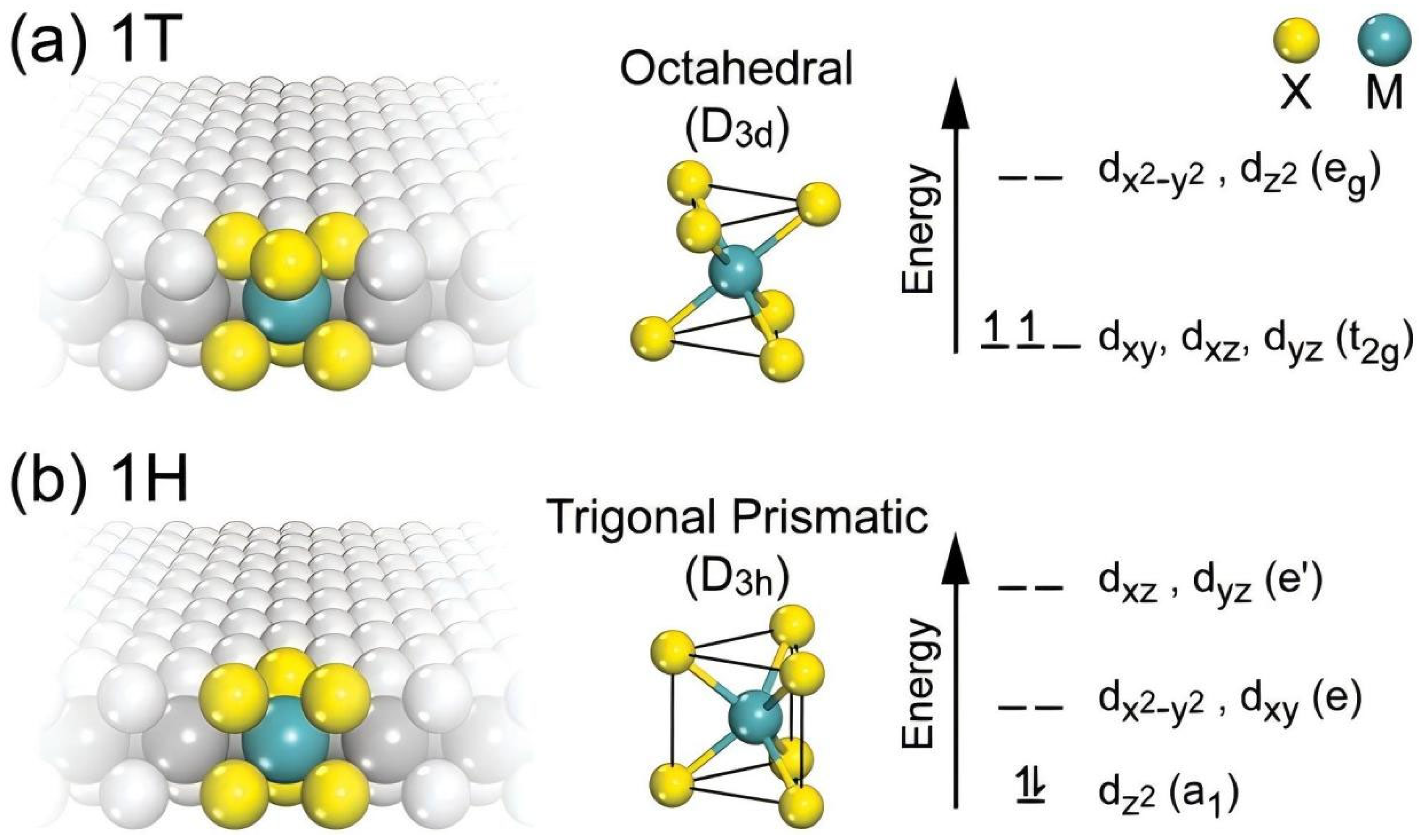
For monolayer of TMD, the atoms stacking along the z-axis are in the XMX form, that is, TM are sandwiched between the two X layers. There are mainly four different phases that have been discovered, that are, 1H, 1T, pentagonal, and tetragonal phase. There are two fundamental phases: 1H and 1T. Among them, the 1H phase exhibits hexagonal symmetry, and the transition metal atoms are coordinated in a trigonal prism. In contrast, the 1T phase has tetragonal symmetry, and the transition metal atoms exist in an octahedral coordination. Reversible phase transition can occur between 2H-MoS2 and 1T-MoS2, and some of the originally catalytically inert basal planes become catalytically active after the 2H → 1T phase transition. Moreover, the 1T phase exhibits excellent structural stability under alkaline electrolysis conditions for HER, enabling sustained catalytic activity. However, the stability of this transformed phase under operating conditions remains a critical concern; the 1T phase is often metastable and may revert to the semiconducting 2H phase during HER, particularly in acidic electrolytes, due to the gradual leaching of intercalated ions or thermally activated relaxation processes. Different from the 1H phase, the top X layer of the 1T phase is rotated by 60°. Apart from the ideal 1T phase, there are distorted 1T phases, such as the 1T′ (also marked as dT and DT) and 1T″ phase. Different from traditional 1H-TMD, the atomic structure of the pentagonal phase ensembles to be wrinkle monolayer. In addition, the tetragonal phase with P4/nmm space group also has a sandwich configuration, which renders low-coordinated non-metal atoms at the basal plane. It is noteworthy that X atoms of 1H- or 1T-TMD are coordinated by six TM atoms forming six-coordination polymers of chalcogenides. However, X atoms in the tetragonal phase are coordinated with four TM atoms, forming X-centered four-coordination polymers. Currently, researchers are trying to enlarge the family of TMD with different structures consisting of varied elements [20]. The differences in electronic structure among various crystal phases directly regulate the charge transfer efficiency and interfacial charge distribution within the material, thereby altering the adsorption capability of active sites toward hydrogen intermediates and achieving precise modulation of ΔGH*. Depending on their compositions and phase structures, 2D TMD display various electronic properties, showing great potential in applications of electronic devices, quantum devices, energy catalysis, etc. [10].

2.2. Physical and Chemical Characteristics of TMD

The inherently low electrical conductivity and narrow band gap of TMDs pose a challenge for their application in electro-catalyzing HER [1,21]. However, these electronic properties can be engineered through various strategies—including stabilization (via covalent bonding or doping), intercalation, and heterostructure construction. Such modifications optimize conductivity and electron transport, thereby creating efficient pathways for electron transfer in the HER [1]. Heterostructures can form directional charge transfer channels via interface energy level matching, accelerating charge separation and transfer. They also optimize the electron cloud density of active sites, bringing ΔGH* closer to the optimal value. In comparison, doping-induced lattice defects break the electronic uniformity, create local charge-rich or deficient sites, adjust the adsorption strength of hydrogen intermediates, and thus regulate ΔGH*. The monolayer TMDs have unique electrical, mechanical, magnetic and optical properties which distinguish them from their bulk counterpart. For instance, while bulk MoS2 is a diamagnetic semiconductor with an indirect band gap of 1.29 eV, 1H-MoS2 is a diamagnetic semiconductor with a direct band gap of 1.90 eV, and 1T-MoS2 is a paramagnetic semimetal. The metallic or semiconducting behaviors of monolayer MoS2 can be explained by a simple energy level model based on the ligand field theory. In MoS2 the metal cation is surrounded by six chalcogen anions with Mo(S)6 molecular geometry. Ligand field splitting of metal d orbitals determines the electronic properties of the compound. Mo ([Kr]4d55s1) supplies four of its six valence shell electrons to bonding states primarily composed of S 3p orbitals. The two other electrons enter into states made by splitting of Mo 4d orbitals. As depicted in Figure 3a, Mo atoms in the 1T crystal are in octahedral coordination (D3d) which results in splitting of 4d orbitals of Mo into a lower triply degenerate band (t2g) and an upper doubly degenerate band (eg). The incomplete occupation of three t2g orbitals by two electrons is responsible for the metallic behavior of 1T-MoS2. In contrast, the Mo atom coordination in 1H-MoS2 is trigonal prismatic (D3h) with ligand-field-induced splitting of Mo 4d orbitals in one non-degenerate orbital (a1) at the lowest energy level followed by two doubly degenerate orbitals (e and e′), as shown in Figure 3b. The highest occupied molecular orbital (HOMO), consisting mainly of Mo dz2 orbitals, is filled with two paired electrons, and the lowest unoccupied molecular orbital (LUMO), consisting mainly of Mo dx2y2 and dxy, is situated 1.9 eV above the HOMO. Therefore, there is a band gap of 1.9 eV in 2H-MoS2 which confirms its semiconducting behaviors [21]. The metallic electronic structure of the 1T phase enables rapid bulk charge transfer, reducing the electron transport resistance of HER. In contrast, the semiconducting 2H phase results in a slow charge transfer rate, leading to a decrease in catalytic activity. Another important trend in TMDs that deserves a special discussion is the change in bandgaps. The bulk bandgap is decreased from sulfides to tellurides in harmony with the increasing metallic character of chalcogens from sulfur to tellurium. By decreasing the number of layers in the crystal of MX2, the bandgap starts to increase from about 5-layer nanosheets. In the limit of the monolayer, in addition to the bandgap widening, an abrupt change from an indirect to a direct bandgap also occurs [21]. Although the kinetics of the HER process on the semiconductor 2H phase are poorer compared to the metallic 1T phase, it has been found that the 1T phase and 1T′/1T″ phase equivalent metallic TMDs can solve the problem of low electrical conductivity of 2H phase TMDs [20].
Both experimental and computational studies indicate that the active sites in 2D TMDs are predominantly located at the material edges, while the basal planes are largely catalytically inert [1]. MoS2 is a typical example from the layered TMDs family of materials. Crystals of MoS2 are composed of vertically stacked, weakly interacting layers held together by van der Waals interactions. Bulk MoS2 is semiconducting with an indirect bandgap of 1.2 eV, whereas single-layer MoS2 is a direct gap semiconductor with a bandgap of 1.8 eV (Figure 4a) [22]. This dimension-dependent bandgap transition characteristic endows it with unique advantages in optoelectronics-related applications. Both coordination modes are based on the three-layer sandwich basic unit of chalcogen atom–metal atom–chalcogen atom (X-M-X), with intralayer M-X bonds predominantly covalent to ensure structural stability. The trigonal prismatic coordination on the left of Figure 4b follows an AbA stacking sequence (uppercase letters represent chalcogen atoms and lowercase letters represent metal atoms); the octahedral (or trigonal antiprismatic) coordination on the right of Figure 4b adopts an AbC stacking sequence, where the arrangement of chalcogen atoms around the metal atom differs. Octahedrally coordinated transition metal centers (D3d) of TMDs form degenerate dz2,x2−y2 (eg) and dyz,xz,xy (t2g) orbitals that can together accommodate the TMDs’ d electrons (a maximum of 6 for group 10 TMDs). On the other hand, the d orbitals of transition metals with trigonal prismatic coordination (D3h) split into three groups, dz2 (a1), dx2−y2,xy (e), and dxz,yz (e′), with a sizeable gap (~1 eV) between the first two groups of orbitals. The thermodynamic stability of the two coordination structures is determined by the d-electron count of the transition metal, which serves as the core reason for the formation of polymorphs (1H and 1T phases) in monolayer TMDs. This provides a structural basis for regulating the electronic properties of materials (such as conductivity and bandgap) and holds significant guiding significance for their applications in fields including electronic devices and catalysis [23]. Consequently, research efforts have focused on engineering active sites into the basal planes through defect creation and edge exposure. These strategies aim to generate highly effective electrocatalytic features, such as corner atoms, kinks, terraces, and other low-coordination sites, which are known to enhance HER activity [1]. The introduction of basal plane defects creates active sites with local charge imbalance in inert regions, which optimizes ΔGH*. Defects also serve as charge transport hubs to enhance charge transfer efficiency. Meanwhile, exposing edge sites increases the number of active sites with optimal ΔGH*, thus synergistically boosting hydrogen evolution catalytic activity.

3. Synthesis of TMDs

TMDs are recognized as promising, cost-effective catalysts for the HER, distinguished by their layered crystal architecture, adjustable electronic structure, and high density of surface active sites. The efficacy of TMD-based HER catalysis is contingent upon the optimization of active site density, charge transfer efficiency, and mass transport kinetics. The layered structure, held together by weak van der Waals interactions, permits facile exfoliation into monolayer or few-layer configurations, which is a strategic advantage for tailoring their catalytic properties. This section organizes the prevailing TMD synthesis strategies, tracing their evolution from basic research tools such as physical exfoliation, through scalable CVD and hydrothermal methods, to precision-oriented atomic-level tuning techniques.

3.1. Physical Exfoliation Method

The physical exfoliation method is a ‘top-down’ strategy for isolating single- or few-layer nanosheets from bulk TMDs. Its core principle involves overcoming interlayer van der Waals forces via mechanical or solvent action. This process preserves the intrinsic crystal structure, making exfoliated TMDs ideal model systems for probing fundamental HER catalytic mechanisms, such as edge site activity and quantum confinement effects.

3.1.1. Mechanical Exfoliation Method

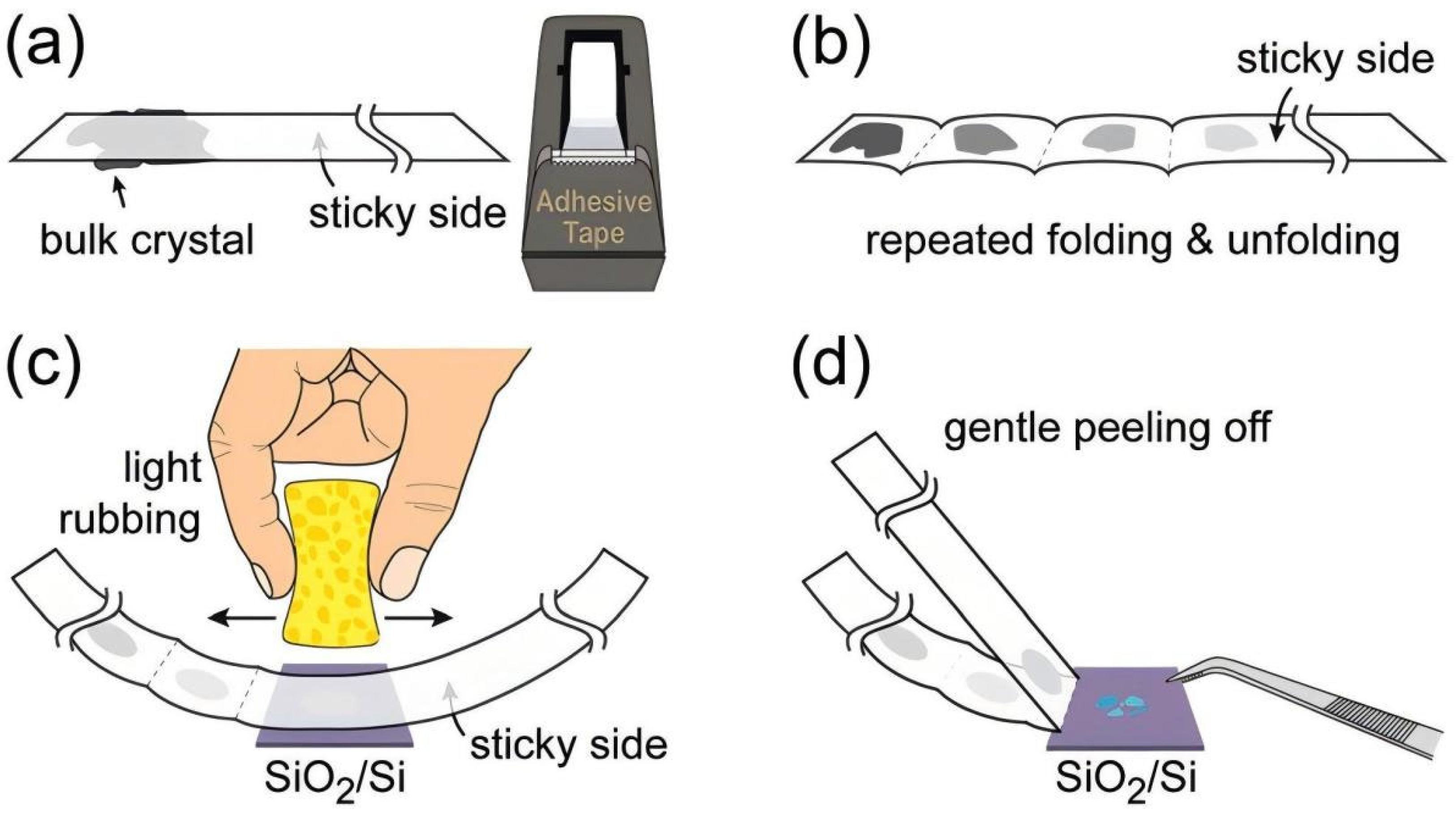
The mechanical exfoliation method involves repeatedly cleaving bulk TMDs (e.g., MoS2, WS2) using adhesive tape. Single- or few-layer regions are subsequently identified and screened using an optical microscope. As shown in Figure 5, a flat 1 cm2 MX2 single crystal was prepared via mechanical exfoliation using adhesive tape. Starting with a bulk crystal (Figure 5a), a thick layer was first peeled off. This layer was then progressively thinned through repeated folding and peeling in a “tape-sandwich” configuration (Figure 5b). The resulting ultrathin flakes were transferred to a SiO2/Si substrate (90 or 285 nm oxide) by pressing and gently rubbing the tape (Figure 5c,d). The tape was subsequently peeled away, leaving the desired MX2 flakes on the substrate for further use (Figure 5d) [21]. Its key advantage is that it introduces no chemical impurities, yielding TMD nanosheets with exceptionally high crystalline integrity. For instance, a MoS2 monolayer produced by mechanical exfoliation demonstrated that its edge sites possess a near-ideal Gibbs free energy for hydrogen adsorption [24]. However, this method suffers from an extremely low yield—producing only a few flakes at a time—with poor control over layer number and size. Consequently, it is suitable only for fundamental research, such as identifying single-atom active sites, and cannot meet the demands of large-scale HER catalyst production.

3.1.2. Liquid Phase Exfoliation Method

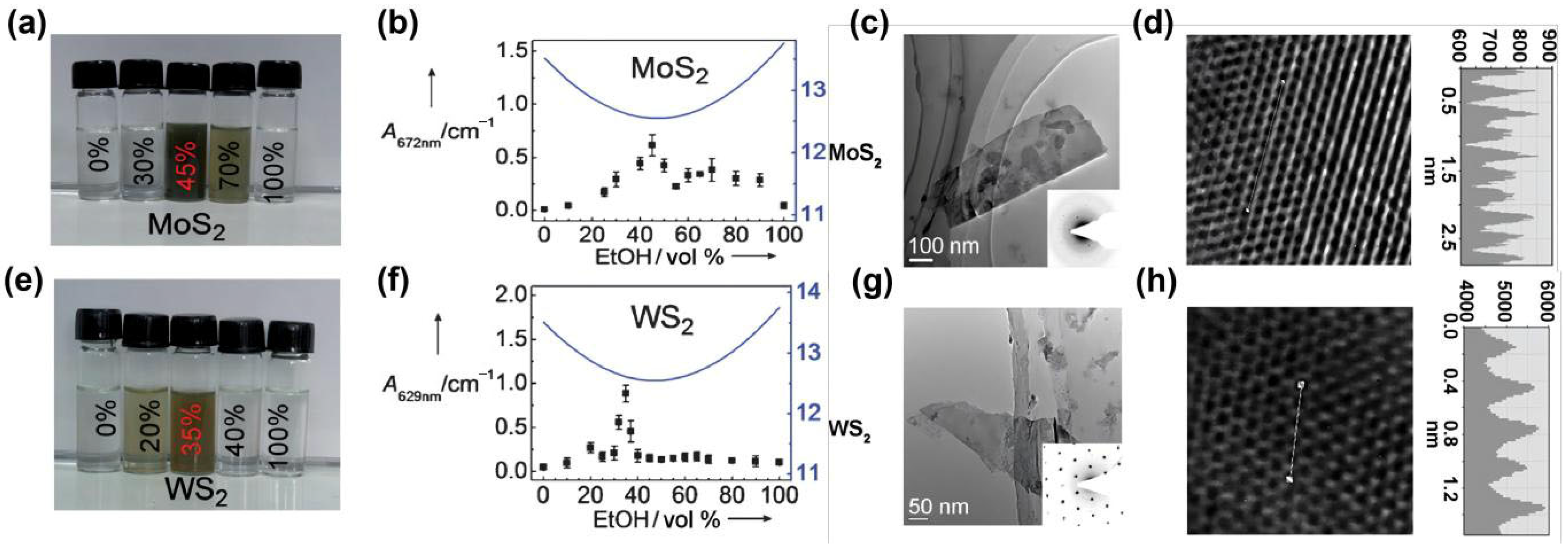
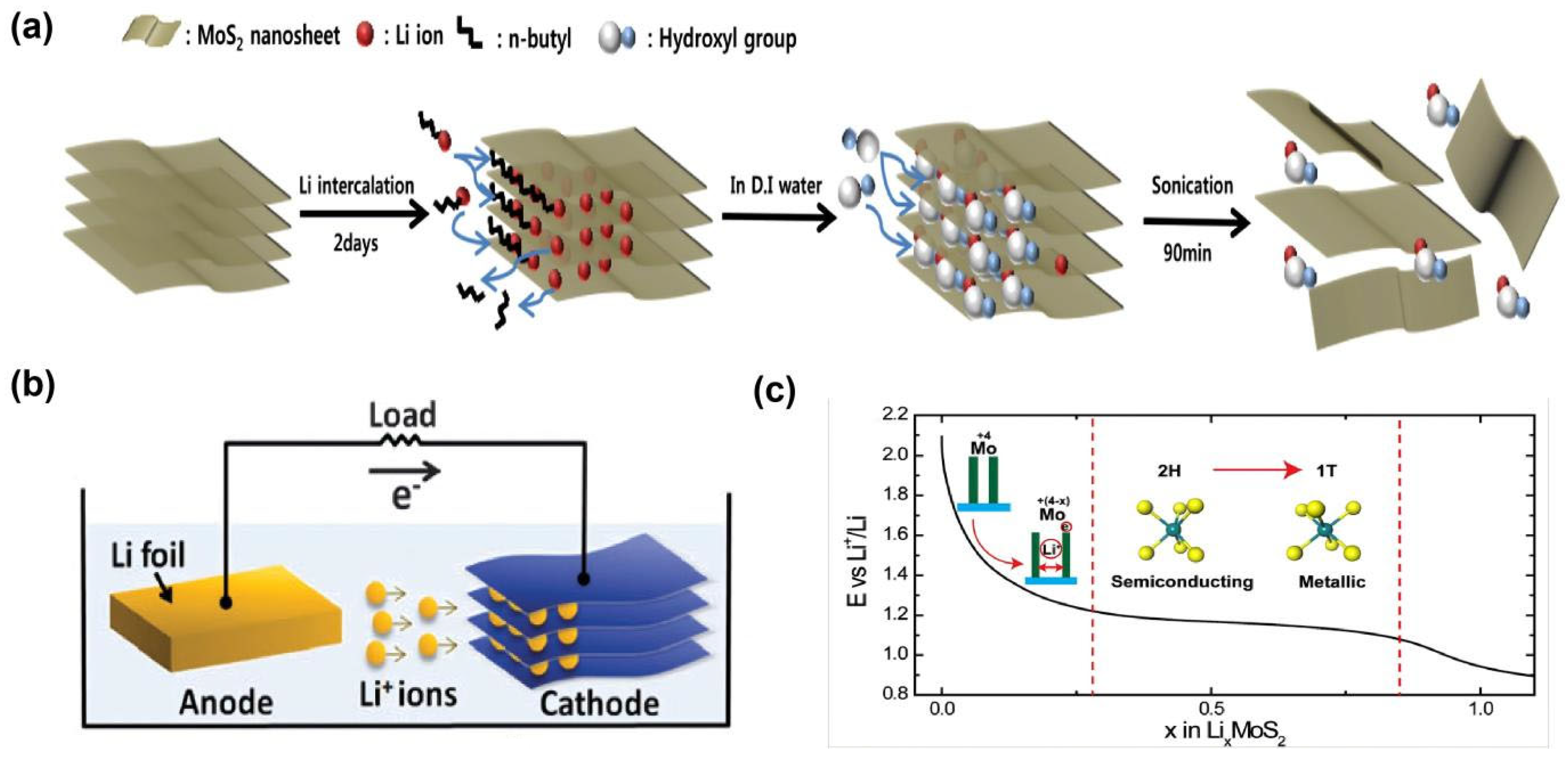
The liquid-phase exfoliation method disperses bulk TMDs in a selected solvent and applies ultrasonic or shear forces to overcome interlayer van der Waals interactions, yielding a suspension of few-layer nanosheets. Effective solvent selection is guided by Hansen Solubility Parameters (HSP). When the solvent’s dispersion (δd), polar (δp), and hydrogen bonding (δh) parameters match those of the TMDs, the interfacial energy is minimized, leading to high exfoliation efficiency [25]. For instance, Zhou et al. demonstrated that a mixture of ethanol and water can be designed to give high solubility for efficient exfoliation of MoS2 and WS2 [26]. To formulate a stable suspension and prevent precipitation, researchers identified an optimal ethanol–water mixing ratio. The efficacy of different solvent ratios is quantified by the interaction radius (Ra), which governs material dispersion. As shown in Figure 6a, a 45% ethanol–water mixture yields the smallest Ra value for MoS2, corresponding to its highest dispersion concentration (Figure 6b). The nanosheets exfoliated with this optimal solvent are thin and flake-like, with lateral dimensions ranging from 100 nm to several microns (Figure 6c). Crucially, Figure 6d confirms that the intrinsic hexagonal lattice structure of MoS2 remains intact after exfoliation. A similar principle applies to WS2, for which a 35% ethanol–water ratio proves most effective, as evidenced in Figure 6e–h. Ion-intercalation-assisted exfoliation represents an advanced liquid-phase strategy. By inserting cations such as Li+ into TMD layers (e.g., via reaction with butyllithium to form LixMoS2), the interlayer spacing expands from 0.62 nm to 0.90–1.00 nm, significantly weakening the van der Waals forces, as shown in Figure 3a, which shows the outline of the procedure in the chemical lithium intercalation and exfoliation method [27]. The rate and efficiency of lithium intercalation can be increased by various strategies. The electrochemical approach has also been employed for lithium intercalation as a fast and controllable method [28]. For this purpose, a set-up similar to the battery test system in a galvanostatic discharge mode with a constant current is used. As shown in Figure 3b, the degree of Li intercalation in the electrochemical method is well-controllable by monitoring the galvanostatic discharge curves [29]. Figure 7 shows the electrode potential (E) of Li+/Li in LixMoS2 as a function of lithium content (x), reflecting the semiconductor-to-metallic (2H to 1T) phase transition and the associated evolution of the material’s electrochemical properties. In this particular method, the bulk TMD is set as cathode and lithium foil as anode in a Li-ion battery setup [30]. The galvanostatic discharge process with optimized conditions induces the lithium intercalation. Zhang’s group effectively optimized the cutoff voltage to prepare few-layered NbSe2 and WSe2 nanosheets [31]. In their related report, single layers of high-yield MoS2, WS2, TiS2, TaS2 and ZrS2 were successfully achieved [31]. This method eases the control of optimum amount of Li ion to be inserted as too little or too much Li insertion brings about serious deterioration in the final product. A limitation of this method is that ultrasonication can introduce structural defects, such as edge fracturing and lattice distortion. Furthermore, some solvents used (e.g., DMF) are highly toxic. While subsequent annealing (300–500 °C, Ar atmosphere) can repair some defects, it must be carefully controlled to preserve beneficial active vacancies.

3.1.3. Ball Milling Method

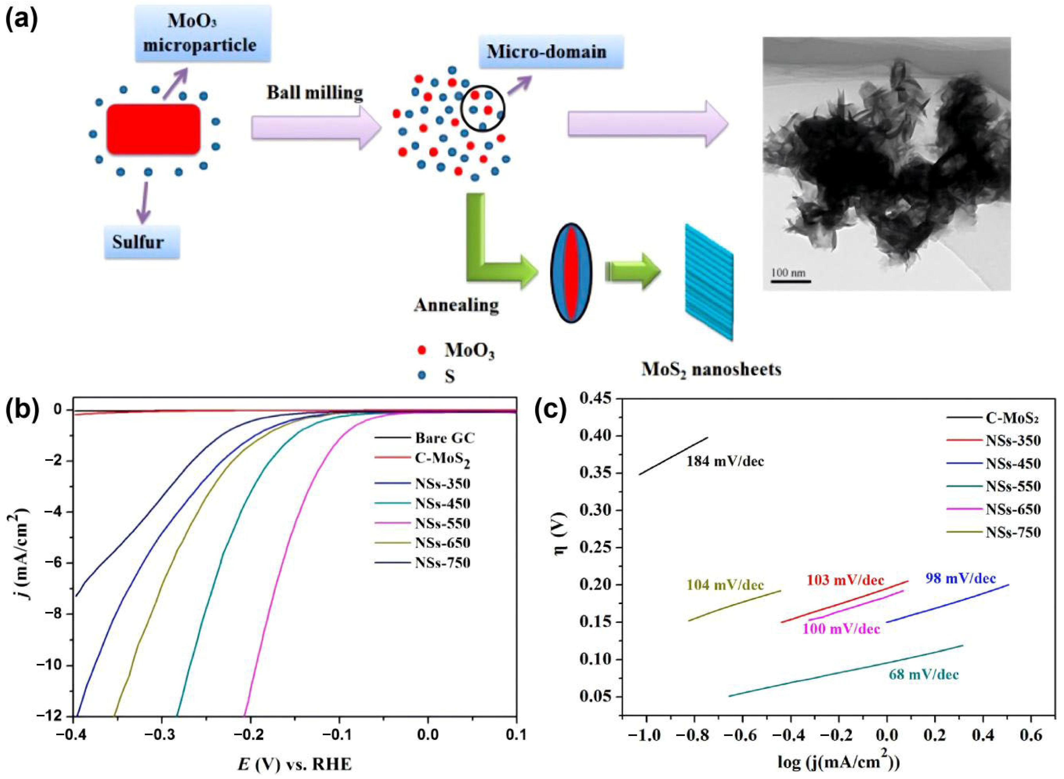
The ball milling method enables the low-cost, large-scale production (kilogram-level yield) of TMDs by utilizing the impact and shear forces of grinding balls to simultaneously exfoliate bulk materials and drive chemical reactions [21,32]. A core advantage of this technique is its capacity for mechanical force-induced defect engineering. For instance, Liao et al. prepared few-layer-MoS2 nanosheets through ball milling pretreatment under specific parameters, followed by electrochemical and ultrasonic exfoliation. Subsequently, sulfur vacancies were introduced into the nanosheets via annealing at 900 °C in a 5% H2/Ar atmosphere. The resulting sample exhibited a HER overpotential of 334 mV at a current density of 10 mA/cm2, achieving the high-value utilization of molybdenite mineral resources [32]. However, ball milling faces challenges in controlling layer thickness and size distribution. As reported by Yi et al., the products typically consist of 5–10 layers with a broad lateral size distribution (100–500 nm) [33]. Furthermore, in some cases, after natural MoS2 undergoes dry ball milling with steel equipment, impurities such as Si (9.4 at.%), Fe (0.27 at.%), and Ca (0.87 at.%) are introduced, and the oxygen content increases significantly. Nevertheless, the trace metallic impurities do not dominate the HER catalytic activity; the improvement of the material’s performance stems from the reduction in its own particle size and the increase in edge active sites [34]. For example, Wilkinson et al. successfully synthesized 2D MoS2-based nanocatalysts with a higher concentration of active sites compared to bulk controls (Figure 8) [35]. The synthesized 2D MoS2 via ball milling has its own ultrathin nanosheets: the extra small thickness of the MoS2 basal plane leads to larger geometric surface areas. The ultra-thin nanosheets produced by ball milling possess a minimal thickness, which results in a larger geometric surface area, further augmenting their catalytic potential.

3.2. Chemical Synthesis Method

3.2.1. Chemical Vapor Deposition (CVD)

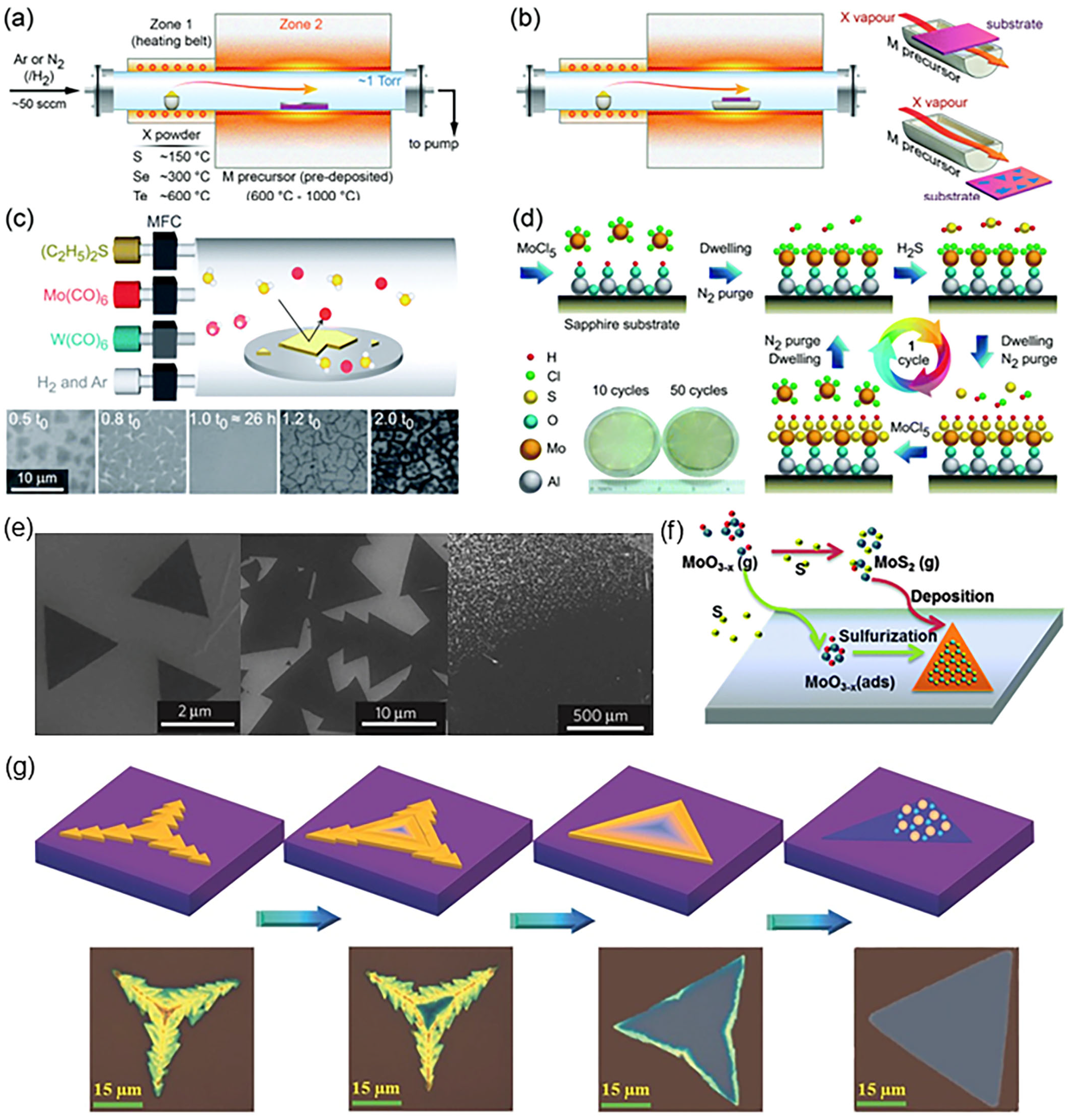
CVD synthesizes TMDs films by transporting transition metal precursors (e.g., MoO3, WCl6) and chalcogen precursors (e.g., S, Se) via a carrier gas (e.g., Ar, N2) to a high-temperature substrate (800–900 °C), where they react. This process is illustrated in Figure 9a: a tubular furnace is divided into a raw material heating zone and a deposition zone. The chalcogen powder is vaporized in the heating zone and carried to the deposition zone, where it reacts with the transition metal precursor to form a film. Figure 9b further simplifies these key steps—precursor transport and substrate growth—providing a visual pathway from gaseous precursors to TMD formation [21]. A principal advantage of CVD is the precise regulation of layer number and crystal phase. For instance, Wang et al. achieved wafer-scale (>4 inch) monolayer MoS2 films by carefully optimizing growth parameters, including precursor ratio, substrate temperature (e.g., 850 °C for MoS2), and carrier gas flow rate [36]. The growth process of these large-area films is detailed in Figure 9c,d, which captures the dynamic evolution from isolated, small nuclei to a continuous, dense layer [37,38]. Figure 9e specifically tracks the growth from initial 2 μm flakes to a final large-scale structure of 500 μm [39]. Furthermore, the optical images in Figure 9g illustrate the coalescence of individual triangular domains into a continuous film, collectively confirming the capability of CVD to produce large-area, high-quality TMDs [40]. These films exhibit exceptional crystallinity, as evidenced by a narrow XRD peak full width at half maximum (FWHM) of <0.1°. This high crystallinity minimizes internal defects and grain boundaries, which significantly enhances both charge carrier mobility and chemical stability. The resulting material also maintains excellent surface flatness, which serves a dual purpose: it provides a structural foundation for subsequent device integration and ensures a uniform current distribution during electrocatalytic reactions. This homogeneity prevents local over-reaction and associated catalyst deactivation, thereby greatly improving the stability and reproducibility of HER performance. The relationship between structure and activity of MoS2 can be analyzed from the growth mechanism, as shown in Figure 9f [41]. The HER activity of MoS2 is largely determined by the structure of its basal plane, which governs the density of active sites. For instance, Ni doping can effectively activate the inert basal plane; when preparing Ni-doped MoS2 via the CVD method, it only needs to regulate the gas-phase partial pressures of molybdenum, sulfur and nickel sources and complete thin-film epitaxial growth on high-temperature substrates, so as to obtain high-crystallinity Ni-MoS2 nanoparticles with controllable doping sites. The product is a bifunctional catalyst for HER/OER in alkaline systems, with an HER overpotential of 156 mV and a Tafel slope below 100 mV·dec−1 [42]. Another key advantage of CVD is the controllable synthesis of heterostructures. By sequentially growing different TMDs (e.g., MoS2/WSe2), it enables the construction of van der Waals heterojunctions, where interfacial charge transfer enhances electron conduction efficiency. Kevin Bogaert et al. reported the preparation of MoS2/WS2 lateral heterostructures via CVD. The core process is as follows: first, high-quality WS2 single crystals are grown at 1100 °C using WO3 and sulfur powder as precursors; then, the precursor is replaced with MoO3 and the growth temperature is adjusted, with compositional rearrangement achieved through Mo atom in-plane diffusion, opening up a brand-new path for the precise synthesis of novel 2D TMD heterostructures [43]. However, CVD faces limitations, including high equipment costs (e.g., for tubular furnaces and precision gas systems), the use of toxic precursors (e.g., H2S, MoO3 vapor) [21], and high reaction temperatures (>800 °C) that can cause substrate interactions such as aluminum diffusion from sapphire, leading to lattice distortions. To address these issues, “salt-assisted CVD” has been developed. For instance, Ambuj Tripathi et al. demonstrated that adding NaCl can lower the MoS2 growth temperature from 850 °C to 650 °C, simultaneously suppressing substrate diffusion and doubling the HER stability of the resulting product [44].

3.2.2. Hydrothermal/Solvent-Thermal Method

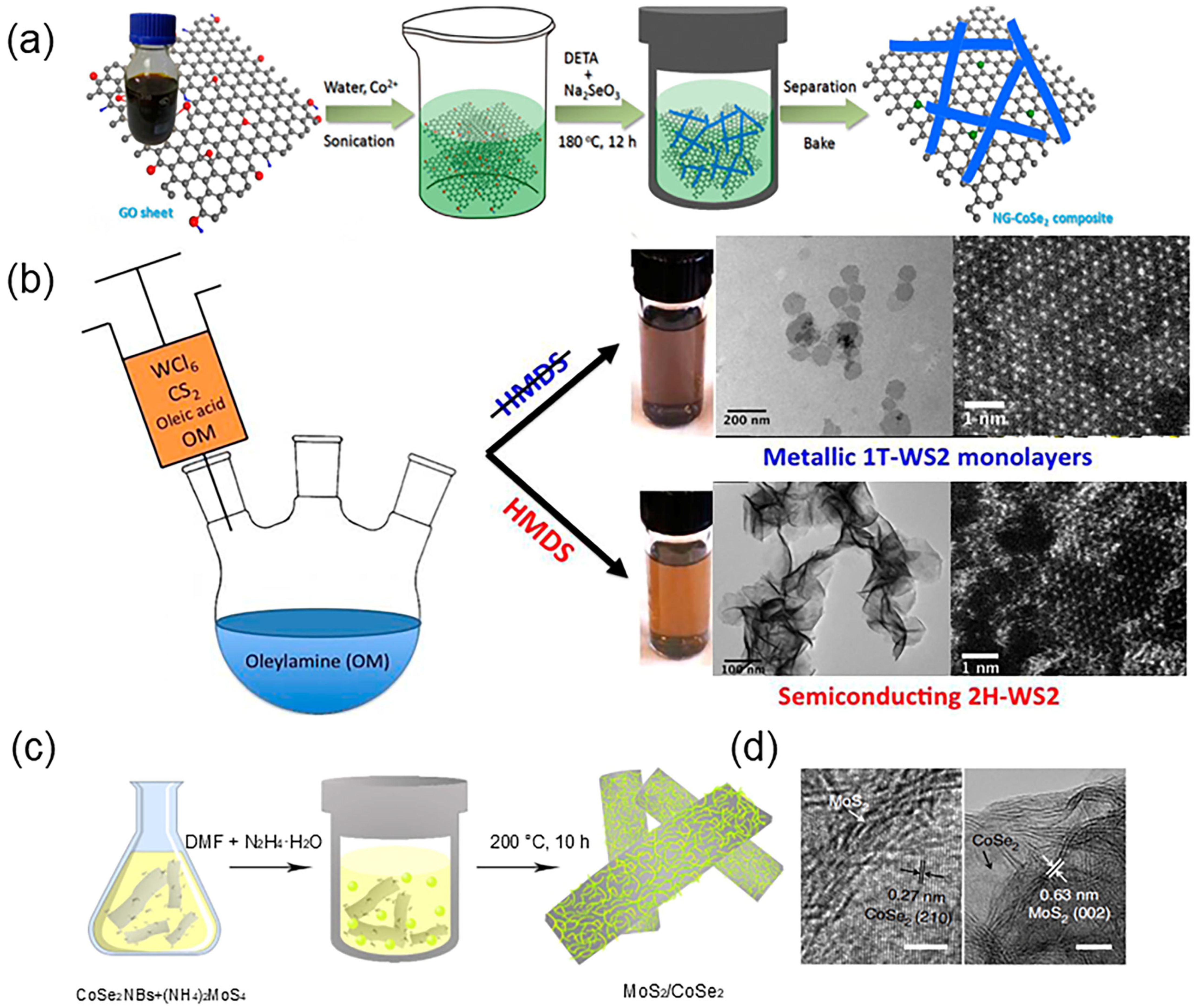
The hydrothermal method employs water as a solvent in a sealed Teflon-lined autoclave to drive heterogeneous reactions, typically at 100–200 °C under autogenous pressure. The solvothermal method extends this approach by replacing water with organic solvents like ethanol or DMF. This substitution leverages the specific physicochemical properties of the solvent (e.g., polarity, viscosity) to control precursor dissolution and transport, while also preventing oxidation, making it suitable for synthesizing non-oxide nanomaterials like TMDs. The hydrothermal/solvothermal method synthesizes TMDs in a sealed reactor (120–250 °C, autogenous pressure) using metal salts (e.g., Na2MoO4, (NH4)2WS4) and sulfur sources (e.g., thiourea, Na2S). Precise morphological control is achieved by optimizing reaction time (4–24 h) and surfactants (e.g., CTAB, PEG) [7,21]. This method offers high yield, rapid reaction kinetics, and moderate operating conditions, making it an ideal, cost-effective route for the large-scale production of homogeneous TMD materials. The hydrothermal method enables precise morphological control, facilitating the synthesis of diverse nanostructures such as MoS2 nanoflowers, MoS2 microspheres, CoS2 nanowires, and CoS2 nanoparticles. These distinct architectures offer significant advantages for electrocatalysis. The 3D hierarchical structure of nanoflowers, the 1D confinement of nanowires, and the small-size effect of nanoparticles collectively yield a high specific surface area—reaching up to several hundred m2/g for some nanoflowers—which provides a wealth of active sites. Furthermore, their unique pore networks and morphological features enhance mass transfer efficiency. The nanostructures grown in a hydrothermal environment typically exhibit good crystallinity and structural stability. This inherent stability helps inhibit material agglomeration and ensures consistent performance over long-term reactions. The combination of high surface area, efficient mass transfer, and robust stability makes these morphologically tailored materials particularly outstanding in electrocatalytic applications. Wang et al. hydrothermally synthesized MoS2 nanoflowers using CTAB as a soft template [45]. These nanoflowers, assembled from single-layer nanosheets, exhibited a high specific surface area of 150 m2/g and an edge site density ten times greater than that of bulk MoS2. This unique structure resulted in excellent HER performance, with an overpotential of 170 mV at 10 mA/cm2 and an j0 of 0.6 × 10⁻² mA/cm2. To further enhance catalytic activity, researchers have extended this method to synthesize TMD-based composites. The core design principle involves integrating TMD nanostructures (e.g., MoS2 nanosheets, CoSe2 nanowires) with conductive and porous substrates like carbon fiber (CF), graphene oxide (GO), or molybdenum mesh. These substrates serve a dual purpose: they act as a stable growth scaffold and significantly improve performance by facilitating electron transport and increasing the exposure of active sites. This design principle is universally applicable. For instance, MoS2 nanosheets grown on CF or GO benefit from enhanced conductivity and a 3D structure that exposes more active sites. Similarly, CoSe2 nanowire arrays on carbon cloth (CoSe2 NW/CC) or nitrogen-doped graphene-supported CoSe2 nanohybrids (NG-CoSe2) demonstrate the versatility of this approach for improving the performance of various TMD materials. Figure 10a illustrates the preparation of an Ni-CoSe2 composite using GO as a substrate. The process involves the ultrasonic dispersion of GO in an aqueous Co2+ solution, followed by the addition of diethylenetriamine (DETA) and Na2SeO3. Subsequent hydrothermal reaction at 180 °C, separation, and calcination yield the final composite, visually demonstrating the “substrate loading and hydrothermal reaction” strategy for TMD-based composites [46]. Beyond composite design with substrates, solvent selection is a critical factor in tuning the properties of TMDs. The solvent directly influences the crystal phase, as demonstrated by Xiao et al., and using ethanol favors the metallic 1T-MoS2 phase (yield > 70%), whereas water primarily yields the semiconducting 2H phase [47]. This phase control directly dictates functional performance: the 1T-MoS2 synthesized in ethanol exhibits higher electrical conductivity, resulting in a HER overpotential 50–80 mV lower than its 2H counterpart. This establishes a clear logical chain from solvent choice to phase structure to catalytic function, underscoring solvent selection as a key variable in function-oriented synthesis. Figure 10b visually validates this principle, showing how different reagents lead to distinct WS2 phases: oleylamine with hexamethyldisilane produces metallic 1T-WS2 monolayers, while other conditions yield semiconducting 2H-WS2 with a flower-like morphology [48]. Leveraging this control, Qian et al. solvothermally synthesized a 1T-MoS2/2H-WS2 heterojunction [2]. The built-in electric field at their interface enhanced charge separation, achieving an HER overpotential of 125 mV at 10 mA/cm2 and a Tafel slope of 44.8 mV/dec in 1 M KOH. This methodology can be extended to create various composites. For instance, Yu’s team used CoSe2/DETA nanoribbons as a scaffold to anchor MoS2 nanosheets, forming a MoS2/CoSe2 composite. Figure 10c illustrates this solvothermal process, where CoSe2 nanoribbons react with (NH4)2MoS4 in a DMF/hydrazine hydrate mixture at 200 °C for 10 h [49]. The HRTEM image in Figure 10d confirms the intimate interface between MoS2(002) and CoSe2(210), providing a structural basis for synergistic performance [49]. However, hydrothermal/solvothermal methods face challenges, including lower product crystallinity and a broad layer number distribution (3–10 layers) compared to CVD [21]. A “hydrothermal-annealing” two-step method effectively addresses this; annealing the precursor at 500 °C in an Ar atmosphere improves MoS2 crystallinity (reducing XRD FWHM from 0.5° to 0.2°), increases conductivity five-fold, and lowers the HER overpotential from 170 mV to 140 mV at 10 mA/cm2 [28]. Furthermore, adding reducing agents like hydrazine hydrate can suppress metal ion oxidation, which, for example, reduced the HER overpotential of Ni-Co-S ternary TMDs to 108 mV at 10 mA/cm2 [1].

3.2.3. Sol–Gel Method

The sol–gel method synthesizes TMD films by first forming a sol from metal salts (e.g., MoCl5) and chalcogen sources (e.g., thiourea) in solution. This sol is then gelled, dried, and finally vulcanized at high temperature (500–600 °C in an H2S atmosphere) to crystallize the TMDs. Its core advantages are procedural simplicity, as it requires no vacuum equipment, and its compatibility with flexible substrates. Large-area films can be deposited on materials like polyimide via spin-coating or doctor-blading for use in flexible HER devices. A one-step sol–gel method was adopted, using dl-mercaptosuccinic acid (MSA) as both a gel accelerator and sulfur source [50]. Cobalt nitrate and chloroauric acid precursors formed a homogeneous sol in an ethanol system, followed by gelation at 60 °C, ethanol aging, and supercritical drying to successfully prepare Au/Co9S8 composite aerogels. The optimized Au/Co9S8-10 exhibits a 3D porous network structure, with 5–10 nm Au nanoparticles uniformly anchored on Co9S8 nanosheets, possessing a BET specific surface area of 145.8 m2/g and a double-layer capacitance of 9.8 mF/cm2. In 1 M KOH alkaline electrolyte, it shows excellent hydrogen evolution performance: an overpotential of only 35 mV at 10 mA/cm2, a Tafel slope of 64 mV/dec, and merely 6% activity loss after 40 h of continuous catalysis, significantly outperforming pure Co9S8 (207 mV) and traditional Co9S8-based catalysts [50]. This advantage stems from the high conductivity of Au reducing charge transfer resistance, combined with the porous structure of the aerogel accelerating mass transfer and exposing sufficient active sites. It provides a feasible strategy for the preparation of low-cost, high-efficiency hydrogen evolution catalysts and expands the application of the sol–gel method in TMD-based composite catalytic materials [51].

3.3. Template Orientation Method

The template-guided method employs preset templates—such as soft templates (e.g., surfactant micelles) or hard templates (e.g., mesoporous SiO2, carbon nanotubes)—to control the morphology, size, and crystal facet exposure of TMDs through spatial confinement and chemical guidance [21,52]. This approach is a core strategy for constructing HER catalysts with a high specific surface area and a high density of active sites.

3.3.1. Soft Template Method

Soft templates utilize micelles formed by the self-assembly of amphiphilic molecules (e.g., CTAB, PEG) as a “growth scaffold” to direct the nucleation of TMDs. This approach not only confines the growth dimensions of TMDs by tailoring the micelle morphology (e.g., spherical or rod-shaped) but also precisely controls the product size through intermolecular interactions. Consequently, it overcomes the issues of aggregation and morphological irregularity common in conventional hydrothermal synthesis, establishing a foundation for fabricating highly ordered, high-performance catalytic structures. A study prepared MoS2 microspheres via a hydrothermal method, using 0.012 mol/L ammonium heptamolybdate as the molybdenum source and 0.336 mol/L thiourea as both the sulfur source and reducing agent [53]. The reaction was conducted at pH = 2 and 160–240 °C for 18–24 h, followed by vacuum drying at 80 °C for 12 h. The resulting product was pure hexagonal 2H-MoS2 with an atomic ratio of S to Mo of approximately 1.94. Both CTAB (0.037 g) and PVP (0.0625 g) acted as dispersants to inhibit the excessive growth of the layered structure. As a cationic surfactant, CTAB dissociates into cationic groups in aqueous solution, which specifically adsorb onto the negatively charged MoS2 particle surfaces through electrostatic interaction to reduce surface tension. Meanwhile, it forms a steric barrier via the steric hindrance effect to prevent particle agglomeration, achieving the optimal dispersion effect. Under the conditions of 220 °C for 24 h, it successfully prepared well-defined MoS2 microspheres with an average diameter of 300 nm. In contrast, PVP, as a nonionic surfactant, has no ionic dissociation property. It only exerts its effect by forming a steric hindrance layer on the MoS2 particle surfaces to amplify the repulsive energy between particles, without the assistance of electrostatic interaction. Thus, its dispersion effect is poorer, resulting in products with larger sizes and irregular morphologies, and its regulatory effect on the layered structure is also weaker than that of CTAB [54].

3.3.2. Hard Template Method

The hard template method utilizes porous materials like SBA-15 mesoporous SiO2 or carbon microspheres as a “mold” to shape TMDs through a process of precursor infiltration, reaction, and template removal. For example, mesoporous WS2 was prepared using SBA-15 as the hard template via an impregnation–hydrothermal (265 °C, 24 h)–HF etching process, exhibiting a BET specific surface area of 254 m2/g and a pore size of approximately 6.6 nm, which significantly increased the exposure of active sites [55]. This hard template synthesis strategy drew on the method for preparing mesoporous TMDs reported by Shi et al. [56]. Furthermore, mesoporous WS2 was compounded with RGO (WG-2 with a WS2-to-GO mass ratio of 1:2) and loaded with 5.82 wt% Pt nanoparticles (size ~2 nm) to obtain the Pt/WG-2 catalyst, which showed drastically improved hydrogen evolution performance. In 0.5 M H2SO4 electrolyte, the catalyst achieved an overpotential of only 57 mV at a current density of 10 mA/cm2, a Tafel slope of 47 mV/dec, and a current density of 143.2 mA/cm2 at an overpotential of 300 mV. It also maintained good stability after 1000 cycles, outperforming most WS2-based catalysts. This performance enhancement is consistent with the HER improvement mechanism of Pt/WS2 composite catalysts reported by Zhang et al., and its high efficiency stems from the synergistic effect between the high specific surface area of mesoporous WS2, the excellent conductivity of RGO, and the high catalytic activity of a small amount of Pt [57].

4. Structural Characterization of TMDs

TMDs like MoS2 and WS2 possess unique layered structures and exceptional physical and chemical properties, granting them broad application prospects in electronics, optoelectronics, and catalysis. Accurate characterization is essential to understand their structure–property relationships and to guide their design and application. This section systematically reviews key characterization methods, focusing on three core aspects: structural morphology, chemical state and elemental composition, and optical properties.

4.1. Structural Morphology Characterization

Structural and morphological characterization directly reveals key attributes of TMD crystals—such as layer stacking, particle size, and surface topography—providing fundamental insight into their crystal structure and micromorphology.

4.1.1. X-Ray Diffraction (XRD)

XRD is a cornerstone non-destructive analytical technique in materials science, operating on the principle of Bragg’s law. By analyzing the position, intensity, and breadth of diffraction peaks, XRD reveals critical information on a material’s crystal structure, lattice parameters, and degree of crystallinity. This makes it particularly valuable for studying 2D materials, where it can identify phase transitions and lattice distortions, thereby guiding structural optimization and application selection. For example, Zhou et al. employed XRD to monitor the structural evolution of MoSe2 during the HER [3]. Their results showed that the MoSe2 characteristic peaks remained stable in a constant electrolyte, confirming structural integrity. However, after seven electrolyte changes, the disappearance of these peaks indicated structural degradation. By correlating these findings with in situ Raman spectroscopy, they verified a mechanism involving the oxidation dissolution and re-adsorption of Mo/Se atoms. This provided direct structural evidence for the concurrent enhancement of HER activity and material stability.
In another study, Guo et al. employed XRD to investigate 1T‴-MoS2-VS, finding that higher sulfur vacancy concentrations (up to 22.9%) induced a low-angle shift in the peak [11]. This shift indicates interlayer spacing expansion, which activates Mo-Mo bonds for charge self-regulation. The technique also confirmed the sample’s high trigonal phase purity (space group P31m). These structural insights—specifically, the controlled interlayer expansion and absence of impurities—were linked to exceptional HER performance, characterized by a low overpotential of 158 mV and a Tafel slope of 74.5 mV dec−1.
Collectively, these studies demonstrate how XRD-derived structural data deepens our understanding of structure–property relationships in 2D materials, providing a foundational basis for their targeted optimization and application.

4.1.2. Scanning Electron Microscopy (SEM)

SEM is a powerful surface characterization technique that utilizes secondary and backscattered electrons to image a sample’s topography. With a resolution ranging from 1 to 10 nanometers, SEM clearly reveals a material’s macroscopic morphology, surface features, and size distribution. Its application extends beyond visualizing a sample’s native state to evaluating synthesis efficacy and correlating morphology with performance. In the realm of 2D materials, SEM is indispensable for providing surface details that are critical for performance optimization.
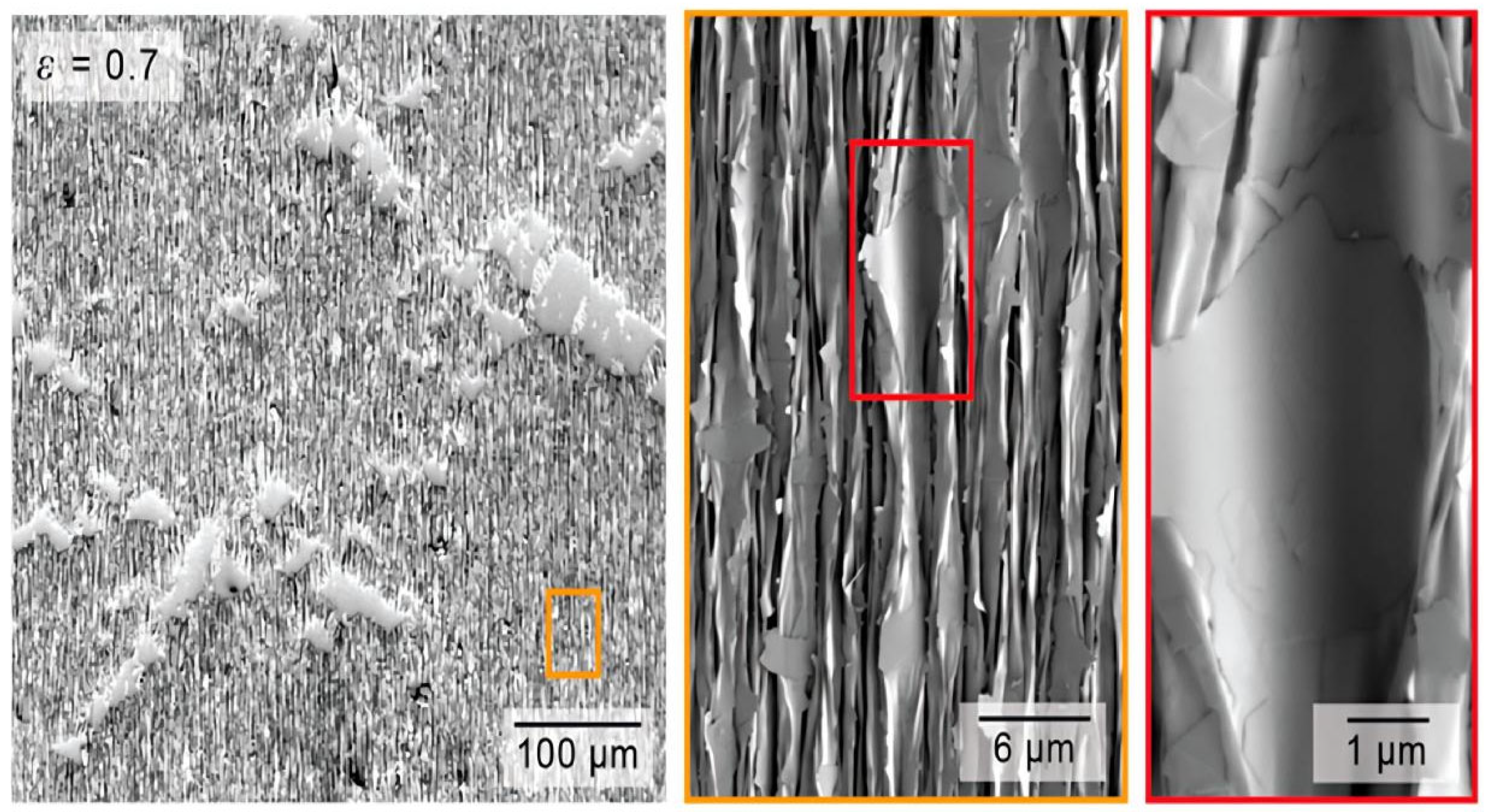
Eng et al. employed SEM to monitor the morphological evolution of MoSe2 upon chemical treatment [58]. While as-grown crystals of MoSe2 showed polygonal stacking, MeLi treatment induced slight layer expansion with some exfoliation debris. In contrast, BuLi treatment caused a more pronounced interlayer separation and extensive wrinkling, increasing its surface area to 74.1 m2/g (vs. 2.33 m2/g for bulk). This superior delamination efficiency provides key microstructural insights for MoSe2’s enhanced HER performance post-exfoliation. Moreover, Rhuy et al. used SEM to investigate Au/PS substrates and MoS2 under varying strain [59]. They observed that the substrate’s wrinkle wavelength increased with the addition of MoS2. Notably, at the strain of ε = 0.7 (Figure 11), MoS2 exhibited an auto-contacting phenomenon, confirming that strain can be used to controllably tune its microstructure and providing a morphological basis for optimizing the HER. Another interesting work is that Cheng et al. utilized SEM to characterize MoS2@ZnIn2S4 heterostructures synthesized via a hydrothermal route [60]. First, Mo precursor reacted with deionized water and nitric acid at 180 °C for 17 h to form MoO3; then MoO3, thioacetamide, and Zn/In salts reacted at 120 °C for 6 h to obtain MoS2@ZnIn2S4. SEM images showed ZnIn2S4 had a well-defined layered structure, and HRTEM confirmed its clear (006) lattice fringe (0.41 nm). This tailored microstructure boosts active site exposure, laying a foundation for enhanced electrocatalytic performance. Collectively, these studies underscore how SEM provides critical morphological understanding, directly guiding the optimization and application of 2D materials.

4.1.3. Transmission Electron Microscopy (TEM)

TEM technology is a key means for studying the microstructure of 2D materials. It utilizes the scattering effect generated by the electron beam passing through the sample to produce high-resolution images, with a resolution that can reach 0.1 nm. Combined with selected area electron diffraction (SAED) technology, TEM can provide a detailed analysis of the crystal structure of 2D materials such as MoS2, including interlayer spacing, defect types (such as vacancies, dislocations), and elemental distribution, offering direct evidence for understanding the origin of material properties. TEM technology can not only be used to observe the interlayer stacking mode but also to identify atomic-level defects, providing direct evidence for studying material properties. For example, Song et al. used TEM technology to characterize the microstructure of MoS2 and Mo0.4W0.6S2 alloys [61]. They found that Mo and W atoms are randomly mixed and share metal sites in the alloy, which provided key structural evidence for understanding the uniformity of the alloy composition and crystal integrity, and supported subsequent research on photoelectric properties. Similarly, Li et al. employed STEM-ADF and EDX to characterize hBN-encapsulated MoS2, observing its atomic arrangement and interface cleanliness [62]. The clean hBN-MoS2 interface minimized Coulomb impurity and phonon scattering, reducing carrier scattering intensity. This structural advantage enabled MoS2 to achieve a high room-temperature mobility of ~100 cm2 V−1 s−1 and low-temperature mobility up to 34,000 cm2 V−1 s−1, providing direct structural evidence for optimizing carrier transport. Additionally, TEM technology can characterize the size, morphology, and dispersibility of SnS nanocrystals, as well as the dispersibility of SnS nanosheets in SnS/N-rGr composite materials [63]. After treatment with atmospheric air plasma, TEM can observe the defect state morphology of SnS films: S vacancies and Sn active sites are formed at 150 W, and oxidation agglomeration appears at 250 W. These characterizations provide direct evidence for the relationship between the structure and electrocatalytic activity of SnS, aiding in the optimization of its HER performance.

4.1.4. High-Resolution Transmission Electron Microscopy (HRTEM)

HRTEM is an advanced imaging modality that extends the capabilities of conventional TEM to the atomic scale. With a resolution capable of reaching the sub-angstrom level, HRTEM enables the direct visualization of atomic arrangements within a crystal lattice. This technique is indispensable in materials science for elucidating atomic-level structure, verifying crystalline integrity, identifying interlayer stacking sequences (e.g., AB or AA), and monitoring structural evolution during phase transitions. Furthermore, HRTEM can resolve atomic configurations at material edges, providing critical insights into the influence of edge effects on material properties.
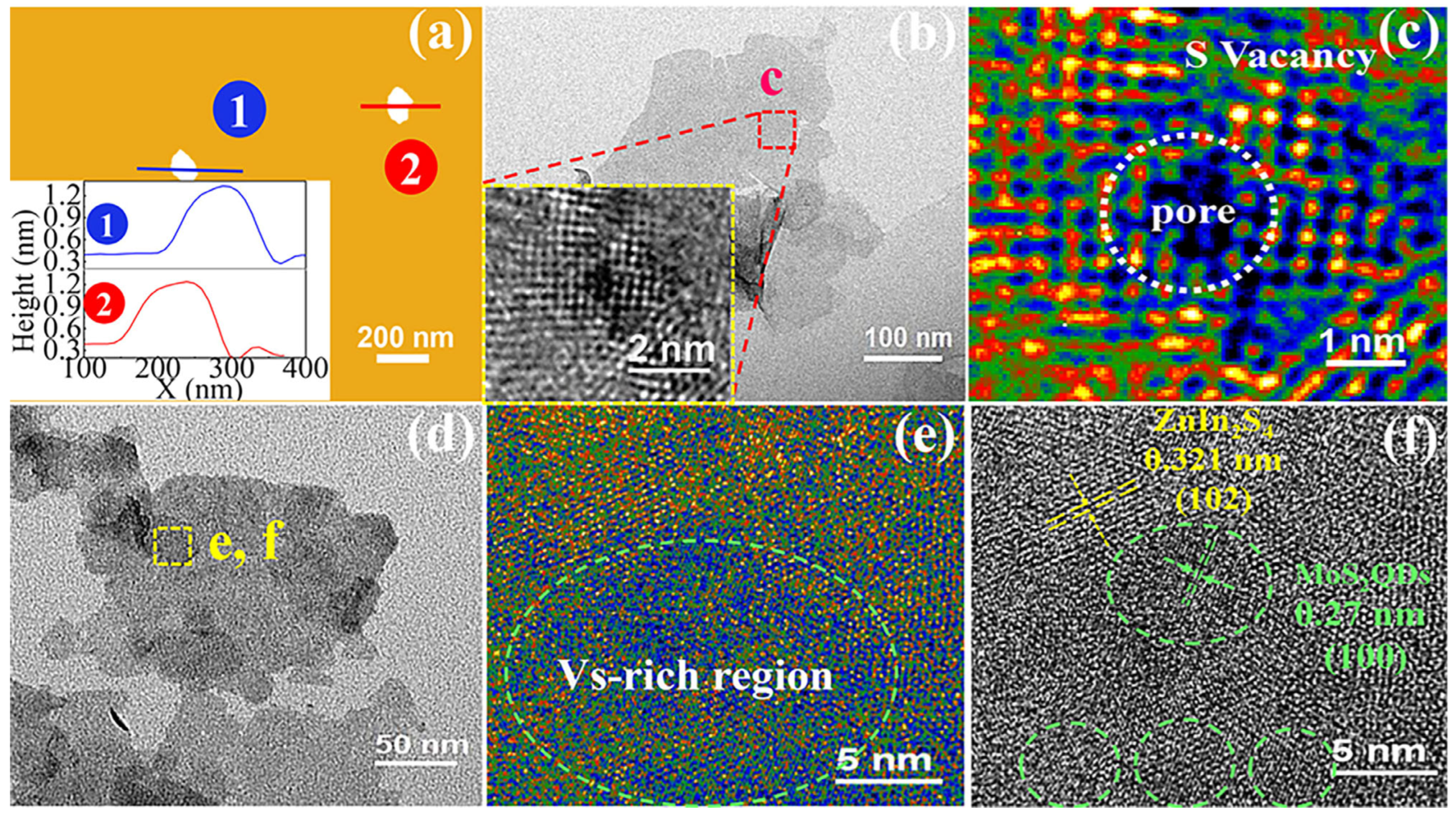
Zhang et al. employed HRTEM to characterize vacancy-rich V_S-ZnIn2S4 [64]. The analysis confirmed the crystal retained its lattice structure without significant distortion, with clear resolution of atomic arrangements around sulfur vacancies, as shown in Figure 12. This structural stability, combined with controlled vacancy distribution, enhances light absorption and charge separation, providing direct evidence that precise vacancy control boosts its photocatalytic hydrogen evolution performance (hydrogen production rate up to 6.884 mmol g−1 h−1). Furthermore, Shemesh et al. employed HRTEM to investigate CdS-Pd4S hetero-nanorods, clearly resolving the lattice matching at their interface [65]. The analysis revealed coherent lattice alignment with minimal strain, as Pd4S(102) lattice fringes (0.216 nm) matched CdS lattice orientations. This structural compatibility facilitates efficient charge transfer across the heterointerface, providing direct evidence that controlled interface engineering optimizes the nanorods’ catalytic performance in HER. Yang et al. used HRTEM to analyze 2D hetero-lamellar composites [17]. They identified distinct lattice fringes corresponding to the (102) planes of ZnIn2S4 (0.32 nm) and the (002) and (100) planes of MoSe2 (0.65 nm and 0.28 nm, respectively), confirming the formation of an intimate sheet-to-sheet heterostructure with a tightly bonded interface. This provided direct evidence that structural integrity and strong interfacial coupling are key to the composite’s exceptional HER rate of 6454 μmol g−1 h−1. Collectively, these studies underscore how HRTEM serves as a pivotal tool, not only for deepening our fundamental understanding of 2D materials but also for guiding their rational design for innovative applications.

4.1.5. Scanning Transmission Electron Microscopy (STEM)

STEM is a high-precision imaging technique that uses an electron beam as a very fine probe to scan the material, achieving imaging by detecting the intensity or phase change in transmitted electrons. STEM not only has the ability to achieve high spatial resolution but also can perform elemental analysis, thus observing the distribution of elements at the atomic scale and distinguishing the positions of different metal atoms. It is particularly suitable for analyzing atomic-level defects such as doping and vacancies in layered structures, as well as studying the regulatory effect of these defects on the electronic structure. STEM technology is also suitable for the 3D structure reconstruction of thin samples, providing a powerful tool for the in-depth understanding of materials.
Xu et al. utilized AC-STEM to characterize the Frenkel-defected monolayer MoS2 (FD-MoS2) catalysts, observing that a fraction of Mo atoms leave their lattice sites to form vacancies and lodge nearby as interstitials, with S vacancies generated prior to Mo migration [66]. Via high-angle annular dark field (HAADF)-STEM imaging, they confirmed the increased Frenkel defect concentration in FD-MoS2-5 (0.85%) compared to FD-MoS2-3 (0.50%), and distinguished it from Pt single-atom doped MoS2 (Pt-MoS2) where Pt replaces Mo atoms. These microstructural insights—especially the unique interstitial Mo and associated vacancies—provided critical evidence for explaining the enhanced HER activity of FD-MoS2 (164 mV overpotential at 10 mA cm−2) superior to pristine MoS2 (358 mV) and Pt-MoS2 (211 mV), bridging the structure–property gap for defect-engineered 2D electrocatalysts. Song et al. used STEM technology to characterize single-layer Mo0.4W0.6S2 alloys [61]. Through STEM-ADF imaging technology, they distinguished Mo and W atoms and confirmed that they are alloyed in nearly 99% random mixing form, with an atomic ratio deviating from the XPS results by less than 5%. Combined with energy-dispersive X-ray spectroscopy (EDX) analysis, they confirmed the presence of W, Mo, and S elements. These findings provided direct microscopic evidence for controlling the composition of Mo1−xWxS2 alloys through vacancies and optimizing the performance of optoelectronic devices. Through these research achievements, STEM technology not only provides a powerful means for understanding the internal microstructure of materials but also offers important scientific bases for the optimization and innovative applications of materials.

4.1.6. Atomic Force Microscopy (AFM)

AFM is a powerful surface analysis technique that characterizes materials by probing nanoscale forces, such as van der Waals and electrostatic interactions, between a sharp tip and the sample surface. It provides atomic-scale resolution (up to 0.1 nm) for precisely measuring the surface morphology, roughness, and thickness of 2D materials. A key advantage of AFM over techniques like TEM is its ability to operate in ambient air or liquid environments without requiring a vacuum or high-energy electron beams, making it an indispensable tool for dimensional control and layer characterization. For example, Zhao et al. utilized AFM to characterize CdS nanosheets (a low-dimensional TMD), measuring their thickness down to ~2 nm—an ultrathin scale achieved via iodine-chalcogen atomic substitution [67]. The AFM analysis confirmed the nanosheets’ submillimeter size and atomic-level thickness uniformity, verifying that atomic substitution enables precise dimensional control. This provides critical microstructural data for CdS’s application in optoelectronic and catalytic systems. Rhuy et al. employed AFM in tapping mode to statistically analyze the thickness and size distribution of transferred multilayer MoS2 thin films [59]. By characterizing hundreds of flakes, they identified typical thicknesses and uniform size distribution, establishing fundamental microstructural baselines. This data is critical for optimizing MoS2’s HER performance—enabling strain engineering and electrochemical activation to achieve efficient hydrogen evolution. Harvey et al. used AFM to analyze liquid-exfoliated GaS nanosheets, statistically determining their thickness and size distributions (mean lengths: 450, 280, 180 nm) [68]. The AFM results revealed that smaller GaS nanosheets expose more edge active sites, reducing the HER onset potential from 0.62 V to 0.48 V vs. RHE. This provides critical microstructural evidence linking PTMC size to enhanced electrocatalytic activity. Collectively, these studies underscore AFM’s critical role in providing quantitative, nanoscale structural data that guides the rational design and application of 2D materials.

4.2. Chemical State and Elemental Composition Characterization

Characterizing the chemical state and elemental composition of TMDs defines the types, concentrations, and valence states of their constituent elements. This information is fundamental to understanding their chemical stability, doping effects, and interface reactions.

4.2.1. Energy Dispersive X-Ray Spectroscopy (EDS)

EDS is a powerful analytical technique that identifies elemental composition by detecting the characteristic X-rays emitted when a material is excited by an electron beam. By measuring the energy and intensity of these signals, EDS enables both qualitative identification of constituent elements (e.g., confirming the presence of Mo, W, and S) and quantitative determination of their atomic ratios (e.g., verifying the 1:2 of Mo:S stoichiometry in MoS2). Frequently coupled with SEM or TEM, EDS can also generate elemental maps to visualize distribution, homogeneity, and potential agglomeration.
Liang et al. employed EDS mapping to characterize laser-patterned VS2 and VS2/MoS2 heterostructures [69]. They confirmed the uniform distribution of V and S in VS2 and delineated the compositional changes induced by laser and acid etching, identifying VSxOy at low laser power and VOz at high power. This provided crucial compositional evidence for the selective etching process and the development of high-performance VS2-contacted MoS2 transistors with a mobility of 3.56 cm2 V−1 s−1. Yang et al. used EDS to verify the high purity of ZnIn2S4, CdIn2S4, and In2S3 [17]. Elemental mapping of a ZnIn2S4/MoSe2 heterostructure revealed the uniform distribution of Zn, In, S, Mo, and Se, corroborating the formation of an intimate sheet-to-sheet interface. These findings supplied key evidence linking compositional uniformity and interfacial contact to the enhanced photocatalytic HER activity of 6454 μmol g−1 h−1. Mukherjee et al. utilized EDS to analyze exfoliated few-layer FePS3 and its rGO-supported composite [70]. The technique confirmed the homogeneous distribution of Fe, P, and S elements with an atomic ratio consistent with the bulk material, and verified the intimate combination of FePS3 and rGO. This compositional evidence supports the material’s excellent HER activity (1.0 ± 0.2 × 10⁻³ A cm−2 exchange current density) and stability across wide pH ranges, laying a foundation for its practical application in electrochemical water splitting. In summary, EDS technology serves as an indispensable microanalytical tool, providing fundamental insights that are critical for optimizing material properties and guiding the development of novel functional materials.

4.2.2. X-Ray Photoelectron Spectroscopy (XPS)

XPS is a powerful surface-sensitive technique that probes the elemental composition and chemical states of a material’s top layers (1–10 nm). By irradiating a sample with X-rays and analyzing the kinetic energy of emitted photoelectrons, XPS provides quantitative data on surface elements and precise information on their oxidation states and local bonding environments. This makes it indispensable for verifying the surface chemistry of 2D TMDs.
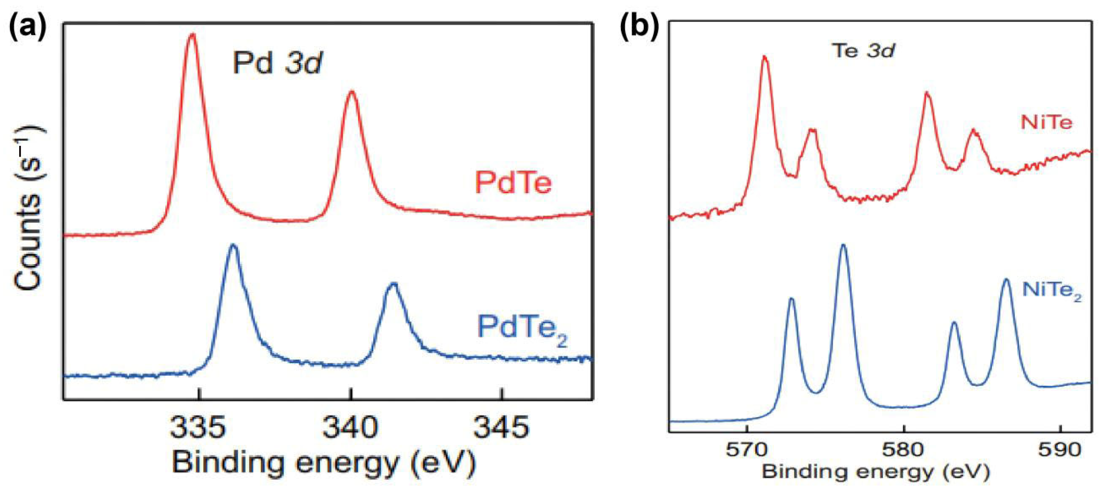
For example, McGlynn et al. employed XPS to investigate the electrochemical activation of 1T′-MoTe2 [71]. Analysis of the Mo 3d and Te 3d core-level spectra revealed only trace oxygen species and no significant shifts in valence states, effectively ruling out surface oxide reduction as the mechanism for enhanced activity. This confirmed the chemical stability of Mo and Te during activation, providing evidence that performance gains—such as a reduced HER overpotential of 178 mV at 10 mA/cm2—stem from electronic structure tuning via hydrogen adsorption. Moreover, Ding et al. used XPS to characterize NiS before and after hydrogen reduction [72]. The Ni 2p spectrum confirmed the transformation into a Ni3S2/NiO hybrid phase. Subsequent near-ambient pressure XPS (NAP-XPS) analysis of the O 1s and S 2p regions identified a synergistic mechanism at the interface, where Ni sites adsorb OH* and S sites adsorb H*. This provided direct electronic structure evidence for the exceptional HER activity, achieving an overpotential of just 95 mV at 10 mA/cm2. Wang et al. utilized XPS to monitor the ion liquid gating of PdTe2 and NiTe2 [73]. They observed significant binding energy shifts in the Pd 3d spectrum upon conversion to PdTe and corresponding valence state changes in the Te 3d spectrum for NiTe2, as shown in Figure 13. Correlated with XRD and STEM data, these XPS results unveiled the structural transformations driven by the self-embedding process, offering key chemical evidence for the emergence of superconductivity in PdTe at 4.3 K. In summary, these studies demonstrate that XPS is not merely an analytical tool but a fundamental technique for uncovering surface chemical phenomena, thereby providing a critical scientific basis for developing new materials and optimizing their functional properties.

4.2.3. X-Ray Absorption Spectroscopy (XAS)

XAS is a powerful technique for probing the local coordination environment and electronic structure of specific elements. By analyzing the absorption edge and the extended fine structure (EXAFS) generated when X-rays are absorbed, XAS provides critical information such as the coordination number of metal atoms (e.g., Mo’s octahedral coordination in MoS2), bond lengths, bond angles, and local structural distortions. Furthermore, it can assess the impact of doping and defects, as well as reveal the density of electronic states, thereby elucidating the connection between electronic structure and chemical activity. A key advantage of XAS is its applicability to both crystalline and amorphous materials, irrespective of their morphology.
For example, Ding et al. employed operando XAS to track the dynamic structural evolution of NiS during the alkaline HER [72]. Analysis of the Ni K-edge spectrum revealed that NiS is first reduced to Ni3S2 at −0.27 V, followed by the formation of a Ni3S2/NiO hybrid phase. Fitting of the EXAFS data confirmed the concomitant process of sulfur vacancy formation and oxygen filling, clarifying the phase transition mechanism. These findings provided direct, time-resolved structural evidence for the material’s exceptional HER activity, which achieves an overpotential of just 95 mV at 10 mA cm−2. This study not only deepens our mechanistic understanding of NiS under reaction conditions but also provides a scientific foundation for designing advanced hydrogen energy conversion materials.

4.3. Optical Property Characterization

Characterizing the optical properties of TMDs—including their light absorption, emission, and electronic transitions—is fundamental to evaluating their potential for optoelectronic devices like photodetectors and light-emitting diodes.

4.3.1. Photoluminescence Spectroscopy (PL)

PL characterizes materials by exciting electrons from the valence to the conduction band using light; the subsequent photon emission as electrons return to the ground state produces a PL spectrum. By analyzing this spectrum’s wavelength and intensity, key material properties can be determined. PL is crucial for measuring bandgap properties—for instance, revealing the direct bandgap of monolayer MoS2 (~1.8 eV) versus the indirect bandgap of multilayer structures. It also assesses crystalline quality, as strong, narrow peaks indicate fewer defects. Furthermore, PL responses to temperature, pressure, or doping provide insights into photophysical processes and guide the design of optoelectronic devices.
For example, Zheng et al. used PL to analyze MoS2 exfoliated using sodium naphthalene [74]. After baking at 200 °C transformed the material into the 2H phase, the sodium-stripped monolayer MoS2 exhibited a distinct PL peak at 668 nm (1.86 eV) with a shoulder at 623 nm (1.99 eV), matching the high quality of mechanically exfoliated samples. In contrast, lithium-stripped samples showed a much weaker PL signal. This demonstrated that the sodium-based process yields higher-quality monolayers, a finding critical for applications like inkjet printing, where control over the exfoliation process enables more uniform and pure materials for enhanced device performance.

4.3.2. Raman Spectroscopy

Raman spectroscopy is a powerful analytical technique that probes molecular vibrations through inelastic light scattering. The unique positions, intensities, and splitting of Raman peaks provide insights into a material’s chemical structure, phase composition (e.g., distinguishing the 2H and 1T phases in TMDs), and interlayer coupling. Known for its rapid acquisition (typically under 5 min), non-destructive nature, and high spatial resolution (~1 µm), Raman spectroscopy is a cornerstone technique for the structural identification and phase characterization of 2D materials, making it ideal for rapid phase screening and studies of interlayer interactions.
For instance, Zhou et al. employed in situ Raman spectroscopy to track the structural evolution of MoSe2 during HER [3]. As the potential changed, they observed the characteristic peaks of the 2H phase alongside the emergence of MoO42− (426 cm−1) and SeO32− (892 cm−1) signals, directly confirming the electro-oxidative dissolution and re-adsorption of Mo/Se species. Correlated with XPS data, these findings provided direct spectroscopic evidence for the enhanced HER activity and stability of MoSe2. Liang et al. used Raman spectroscopy to characterize VS2/MoS2 heterostructures [69]. The distinct Raman fingerprints of VS2 (121, 165 cm−1) and MoS2 (384, 404 cm−1) confirmed the formation of both lateral and vertical heterostructures. Furthermore, Raman mapping clearly delineated the spatial distribution and boundaries between the two materials. This structural verification was critical for fabricating high-performance VS2-contacted MoS2 transistors, which achieved a mobility of 3.56 cm2 V−1 s−1.

5. Regulation Strategies of TMDs for Enhancing HER Performance

In recent years, TMDs have garnered significant attention as promising electrocatalysts for HER, primarily due to their potential to supplant precious metal-based catalysts. While several comprehensive reviews have systematically tabulated the HER performance of various TMDs—including metrics such as electrolyte, overpotential, Tafel slope, stability, and catalyst loading—a critical gap remains [75,76,77]. To date, there has been no systematic summary dedicated to the strategies employed for modulating TMDs to further enhance their catalytic activity. This review aims to address this gap by providing a focused and systematic overview of the key modulation strategies for high-performance TMD-based HER electrocatalysts.

5.1. Doping Regulation Strategy

Doping represents a powerful strategy for optimizing electrocatalysts by modulating their electronic structure and tailoring surface charge distribution [78,79]. A primary objective is to engineer the ΔGH* to approach the optimal value of 0 eV. This optimization balances the hydrogen interaction at the catalyst surface, preventing both excessively strong adsorption that impedes hydrogen desorption and overly weak adsorption that limits initial proton binding. Furthermore, doping introduces and activates sites at edges and defects, thereby increasing the density of active sites and enhancing the intrinsic catalytic efficiency. It also improves electrical conductivity, accelerates electron transfer kinetics, and can bolster the catalyst’s stability and corrosion resistance in harsh electrolytes through the incorporation of heteroatoms. Doping strategies are broadly classified into metal [80,81], non-metal [82,83], and mixed doping [84,85].
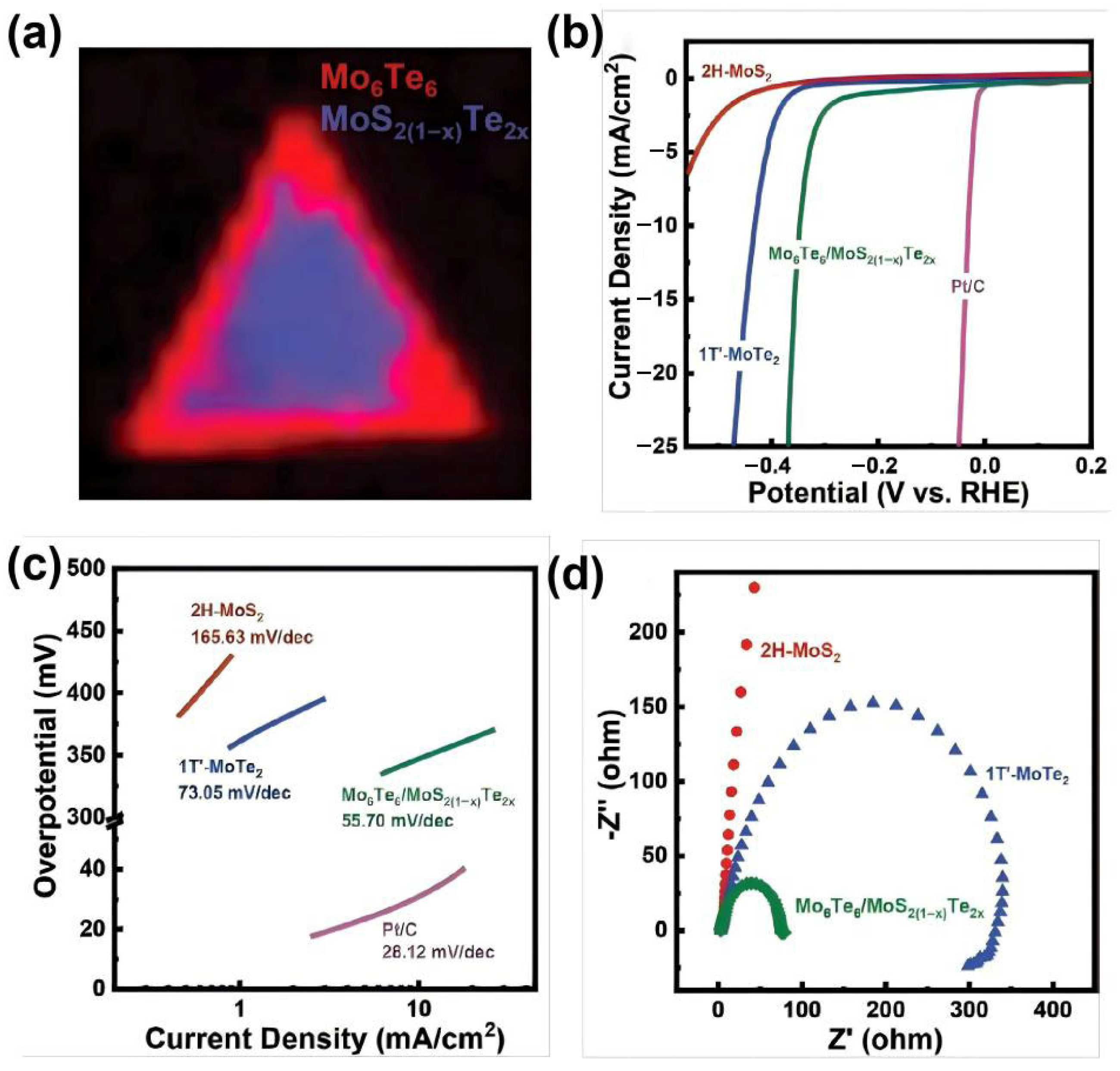
From a mechanistic perspective, doping directly modifies the electronic structure of TMDs through orbital hybridization and charge redistribution. Metal dopants introduce additional d-orbitals that rehybridize with the host metal’s d-bands, shifting the d-band center relative to the Fermi level and thereby optimizing ΔGH* on adjacent sulfur edges. Non-metal dopants substitute chalcogen sites, creating localized mid-gap states that facilitate electron transfer from the catalyst bulk to surface active sites. This dual modulation—optimizing ΔGH* while enhancing charge transfer kinetics—underpins the superior HER activity observed in doped TMD systems. For instance, Lu et al. demonstrated significantly improved HER activity through tellurium (Te) doping [86,87,88]. As shown in Figure 14a, based on the intensity distribution of the MoS2 characteristic peaks, the spatial variation in the chemical composition of the heterostructure can be intuitively visualized. Specifically, the intensities of the characteristic peaks at 155 cm−1 and 246 cm−1, which are assigned to Mo6Te6, are significantly enhanced in the edge nanoribbon region. In contrast, the central 2D region is dominated by the peaks at 233 cm−1 (characteristic of MoTe2) and 382 cm−1/403 cm−1 (characteristic of MoS2), which correspond to the MoS2(1−x)Te2x phase. These findings further corroborate the formation of a distinct boundary between the quasi 1D Mo6Te6 nanoribbons and the 2D MoS2(1−x)Te2x basal plane, thus verifying the successful fabrication of the target 1D/2D heterostructure. Electrochemical performance was evaluated in 0.5 M H2SO4 using a standard three-electrode system, as shown in Figure 14b–d. The heterostructure synthesized at 820 °C delivered superior performance compared to pristine 2H-MoS2, 1T′-MoTe2, and a Pt/C benchmark. This material achieved a low overpotential of −320 mV at a current density of 10 mA cm−2 (a 50% reduction versus pristine MoS2), a Tafel slope of 55.7 mV dec−1 (a 33.3% improvement), and a charge transfer resistance (Rct) of just 70 Ω (merely 3% of the original value). These results conclusively show that Te doping enhances catalytic activity by favorably reducing the ΔGH* on the sulfur edges.
A landmark study by Liu et al. on the phosphorus (P) doping of MoS2 revealed that this non-metal modification simultaneously accomplishes three critical objectives: activation of the inert basal plane, improved charge carrier transport, and expansion of the interlayer distance [83,89]. This multi-faceted enhancement provides a universal blueprint for elevating the catalytic performance of various TMDs (e.g., WS2, CoS2). Electrochemical measurements in 0.5 M H2SO4 showed a systematic improvement in HER activity with increasing P content. The exceptional performance of the P3 sample is highlighted by its Tafel slope of 34 mV/dec, approaching the Pt/C benchmark (30 mV/dec). Further analyses confirm the overall enhancement: a reduced charge-transfer resistance, increased charge carrier density, and a five-fold higher double-layer capacitance (56 vs. 11 mF cm−2), signifying a greatly expanded electrochemically active surface area. Most importantly, the turnover frequency (TOF) at 100 mV overpotential for P3 was 1.4 H2/s, which is 12.7 times greater than that of pristine MoS2 (0.11 H2/s), unequivocally confirming a dramatic improvement in the intrinsic activity of the catalytic sites [90].
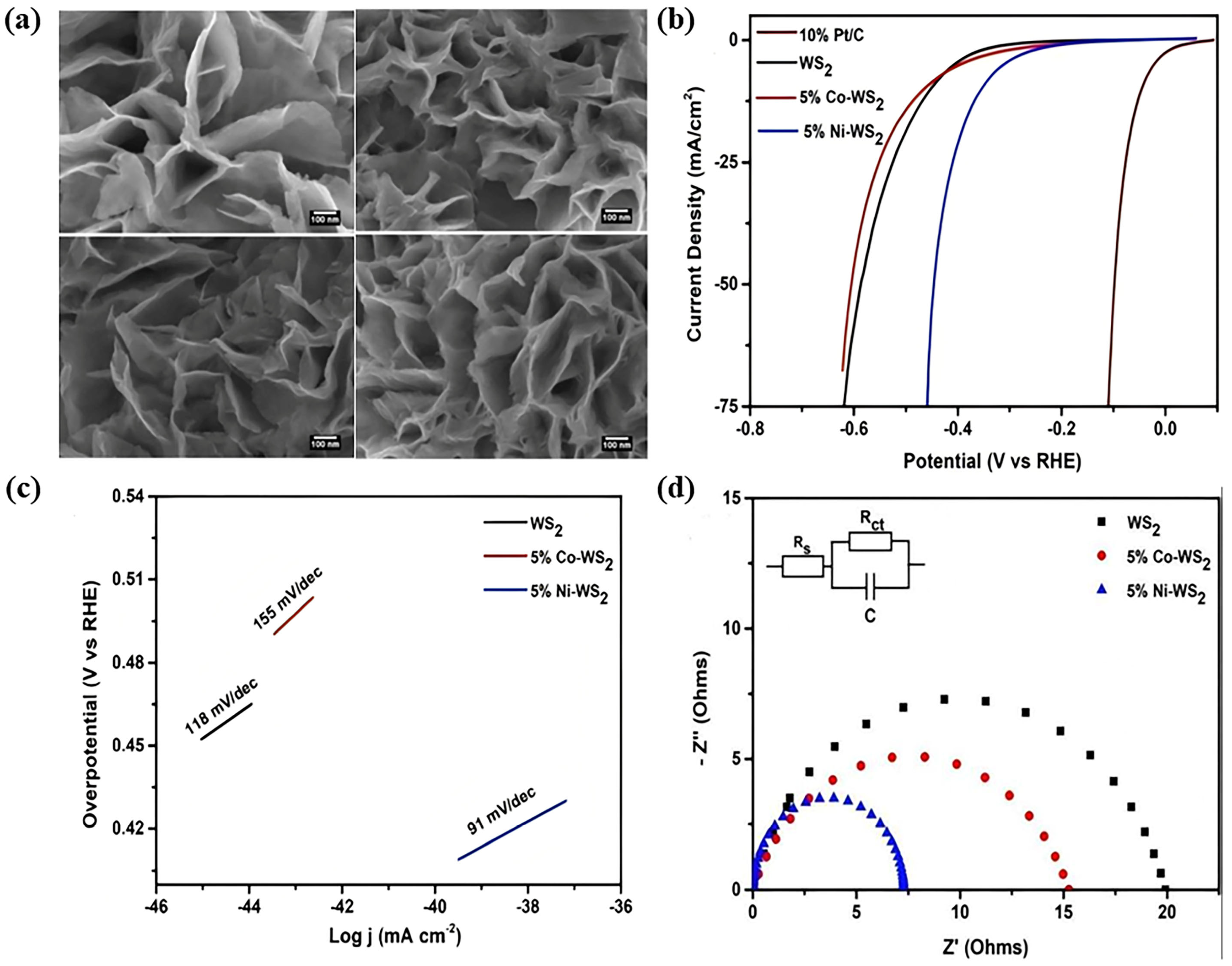
In a study on mixed doping, Anju Joseph et al. synthesized Co- and Ni-substituted WS2 nanoflakes via a hydrothermal method [91,92]. By introducing specific molar ratios of cobalt and nickel precursors into a tungsten-containing solution, they prepared WS2 with varying Ni content (1%, 5%, and 15%). As shown in Figure 15a, FESEM images reveal that the pristine WS2 and all metal-substituted counterparts—including 5% Co-doped WS2 as well as 1%, 5%, and 15% Ni-doped WS2—display distinctly layered and well-ordered morphologies, characterized by interwoven, curled nanosheets. No particle agglomeration or bulk aggregation is observed in any of these samples. Notably, their curling degree and crisscross distribution characteristics are highly consistent with those of the pristine WS2, without the occurrence of particle adhesion, lamellar fracture, or other novel morphological features. These observations directly demonstrate that the substitution of Co and Ni heteroatoms does not alter the intrinsic layered morphology of WS2. Electrocatalytic evaluation demonstrated that the 5% Ni-substituted WS2 outperformed both the pristine and 5% Co-substituted samples, exhibiting lower onset potentials, smaller overpotentials, reduced Tafel slopes, and lower charge-transfer resistance. HER performance improved with increasing Ni content, with the 15% Ni-WS2 sample achieving optimal results: an overpotential of 320 mV (vs. RHE) at 10 mA cm−2 (Figure 15b), a Tafel slope of 82 mV dec−1 (Figure 15c), a charge-transfer resistance of 60 Ω (Figure 15d), and excellent long-term stability. This hydrothermal synthesis presents a viable and economical strategy for developing efficient HER electrocatalysts with potential applications in renewable energy technologies like water electrolysis.

5.2. Ion-Embedded Structural Regulation Strategy

The ion insertion strategy is a structural regulation technique that modulates material properties through the reversible intercalation or substitution of ions (e.g., Li+, Na+, K+) within a material’s lattice or channels [93]. This process can precisely tune the crystal structure, electronic state, and interface properties, thereby enhancing key physicochemical characteristics such as electrical conductivity, catalytic activity, and stability, while also promoting ion migration and increasing the density of active sites [94]. The mechanistic origin of enhanced HER activity in ion-intercalated TMDs lies in the charge transfer from intercalated ions to the host lattice. Upon intercalation, electrons are donated to the TMD’s conduction band, filling previously empty metal d-orbitals.
A prominent example is the work by Wu et al., who synthesized metallic 1T-phase MoS2 by electrochemically lithiating semiconducting 2H-MoS2 [30,95,96]. As previously noted, the 1T phase exhibits superior metallic conductivity, which facilitates efficient electron transport and creates abundant catalytic active sites. This transformation is driven by the formation of a distorted octahedral coordination geometry with short Mo-Mo bonds upon Li+ intercalation. As shown in Figure 16, XPS results indicate that the Mo 3d binding energy of 1T-phase and amorphous MoS2 is approximately 0.9 eV lower than that of the 2H counterpart, a distinct signature indicative of their metallic electronic configurations. After electrochemical reactions, the Mo 3d peak of 1T-MoS2 exhibits a pronounced positive shift, moving from an initial value of 228.6 eV back to 229.5 eV. This observation provides direct evidence that the 1T phase undergoes a surface phase transition to the 2H phase under electrochemical conditions. In contrast, the amorphous MoS2 only shows a negligible and stable binding energy shift of ~0.7 eV, verifying its superior structural stability during the reaction. Complementary analysis of the S 2p spectra further corroborates that the phase transformation is predominantly governed by the evolution of the chemical environment of Mo species, rather than that of S. Both cyclic voltammetry (CV, Figure 16a) and linear sweep voltammetry (LSV, Figure 16b) show that 1T-MoS2 and amorphous MoS2 (Am-MoS2) achieve significantly higher current densities than the 2H phase at the same potential. Initially, the activity of 1T-MoS2 is comparable to that of Am-MoS2. Furthermore, the Tafel slopes of the 1T and amorphous phases are substantially lower than that of the 2H phase (Figure 16d), indicating faster HER kinetics and more efficient electron transfer and hydrogen desorption processes. However, a key difference emerges in their long-term stability. Chronopotentiometry tests (Figure 16e) reveal that while the potential of Am-MoS2 remains stable over 24 h, the potential of 1T-MoS2 gradually increases, signaling a continuous loss of activity. This degradation was subsequently attributed to the gradual dissolution of Li+ ions from the 1T-MoS2 lattice into the electrolyte during operation, causing a partial phase reversion to the less active 2H structure. In contrast, the amorphous Am-MoS2 phase maintains its structural integrity and high HER activity, underscoring its superior operational stability.

5.3. Surface Modification Strategy

Surface modification is a strategy for optimizing material properties—such as catalytic activity and corrosion resistance—by structurally or chemically engineering the surface layer (from monolayer to micron thickness) without altering the bulk material. Through techniques like structural reconstruction, chemical functionalization, or functional assembly, this approach tailors the surface’s physicochemical state and interfacial interactions. This allows for the optimization of key characteristics like surface charge and affinity, thereby improving how the material interacts with its environment [97]. The mechanism by which surface modification enhances HER activity involves interfacial charge redistribution and the creation of new active sites. When noble metal nanoparticles are deposited on TMD surfaces, the work function difference between the metal and the semiconductor drives spontaneous electron transfer across the interface. This charge transfer not only enriches the electron density at the TMD surface but also polarizes the adjacent sulfur or metal atoms, optimizing their ΔGH*. Additionally, the nanoparticle–TMD interface itself can serve as a unique active site with modified electronic properties distinct from either component alone. The result is a synergistic enhancement where both the number of active sites (through basal plane activation) and their intrinsic activity (through electronic modulation) are simultaneously improved.
The efficacy of this strategy is demonstrated in the enhancement of the electrocatalytic activity of MoS2. Research has shown that this activity is intrinsically linked to the density of exposed active sites, particularly edge sites. A significant increase in active sites was achieved by decorating MoS2 nanosheets with well-dispersed gold nanoparticles (AuNPs) [98,99]. The high basal-to-edge ratio of MoS2 provides ample anchoring points for the AuNPs. Furthermore, interfacial charge transfer from the AuNPs to MoS2 enhances the n-type conductivity of the semiconductor, which in turn further activates the adjacent edge sites [100]. Quantitative analysis confirms that the HER activity of the MoS2/AuNP composite, measured by the overpotential at 10 mA cm−2, exhibits a linear correlation with AuNP dispersion density. This underscores the critical role of the synergistic effect between the nanoparticles and the MoS2 edges. The underlying structural properties of MoS2 also contribute to its performance. In the composite electrode, the layered stacking of MoS2 nanosheets creates a highly porous, low-density (1.81 g cm−3) architecture with good wettability (contact angle ~89°), facilitating electrolyte penetration. This structure, combined with a high double-layer capacitance (~50 F g−1), results in a large electrochemically active surface area, providing abundant pathways for mass and charge transport during HER. The HER performance is highly dependent on both AuNP loading and the number of MoS2 layers. An optimal AuNP loading (~4.56 × 10¹¹ particles cm−2) yields the best performance, with an overpotential of −0.21 V and a Tafel slope of 115 mV dec−1, surpassing similar composites with MoSe2 and WSe2. However, excessive loading leads to nanoparticle agglomeration, which reduces the number of active sites and diminishes activity—a phenomenon consistent with observations in other systems like graphene-supported AuNPs [100]. Additionally, monolayer or few-layer MoS2 nanosheets outperform their bulk counterparts due to shortened electron transport paths and a higher proportion of exposed edge sites.

5.4. Moiré Superlattice Strategy

The Moiré superlattice strategy involves the precise stacking of two or more atomically flat 2D materials (e.g., graphene or TMDs) with controlled twist angles, lattice mismatch, or in-plane strain. This creates a synergistic geometric interference effect. Its defining feature is the emergence of a “secondary macro cycle”—a moiré periodicity typically spanning tens to hundreds of nanometers—that is much larger than the original atomic lattice. This long-range periodicity, governed by weak interlayer van der Waals coupling while preserving the integrity of the individual monolayers, can induce novel physical phenomena, effectively creating artificial functional structures with tailored properties [101]. The exceptional HER activity of Moiré superlattices arises from two interrelated mechanisms: strain-induced electronic modulation and interlayer charge hybridization. The lattice mismatch or rotational misalignment between stacked layers generates periodic strain fields within the TMD lattice. This strain locally alters metal–chalcogen bond lengths and angles, shifting the d-band center and creating spatial variations in ΔGH* across the moiré unit cell. Concurrently, the interlayer coupling—even if weak—hybridizes the electronic wavefunctions of the two layers, leading to the formation of flat bands and enhanced density of states near the Fermi level. This electronic reconstruction facilitates rapid charge transfer and provides a high concentration of charge carriers to participate in the HER.
A compelling application of this strategy is demonstrated by Xie et al., who synthesized a WS2 moiré superlattice via a one-step hydrothermal method [102,103]. As illustrated in Figure 17, the resulting material exhibited exceptional electrocatalytic performance for the HER in a 0.5 M H2SO4 electrolyte. It achieved a low overpotential of 60 mV at 10 mA cm−2, outperforming conventional 2H and 1T′ phase WS2 nanosheets (Figure 17b). The Tafel slope of 40 mV/dec indicated a Volmer– Heyrovsky reaction mechanism (Figure 17c). The superior performance is attributed to several key characteristics of the moiré superlattice. Its electrochemically active surface area (ECSA) was measured at 396.6 cm2 (Figure 17d), significantly larger than the other WS2 samples, suggesting a greater density of active sites. As shown in Figure 17a, FESEM shows that the sample exhibits a large-scale uniform conical nanoarray structure, with an average width of about 200 nm. Its open-space design provides ample channels for electrolyte ion transport, and facilitates subsequent infiltration and gas desorption, fully meeting the requirements for electrocatalytic hydrogen evolution, confirming that a one-pot hydrothermal method can achieve scalable fabrication of this material. Furthermore, the surface exhibited simultaneous super-hydrophilicity (contact angle of 9.1°) and super-hydrophobicity (contact angle of 86°), which facilitates electrolyte penetration and rapid bubble release, thereby accelerating HER kinetics.
Table 1 presents a systematic assessment of four distinct strategies to improve the electrocatalytic performance of 2D TMDs, including MoS2 and WS2. By comparing key metrics such as catalytic activity, stability, cost-effectiveness, and process feasibility, this analysis establishes a critical framework for informed decision-making in material design.
A comparative evaluation of these strategies reveals a clear performance–cost trade-off. Doping regulation enhances activity significantly and is widely applicable, yet it faces stability dependencies and moderate-to-high costs. Ion intercalation is a low-cost route to substantial activity gains, such as inducing phase transitions, but it suffers from poor stability and rapid activity decay. Surface modification excels in interfacial engineering with high activity and good stability, though it is often costly and prone to agglomeration. Moiré superlattices represent the performance pinnacle, offering exceptional activity and stability through unique electronic regulation, but their fabrication is atomically precise, costly, and not readily scalable. Consequently, Moiré superlattices stand out for ultrahigh-performance applications where cost and scalability are not priorities, such as fundamental catalytic mechanism studies or high-end low-volume devices, delivering unparalleled activity and stability by uniquely modulating electronic structure and leveraging strain effects to represent the performance pinnacle of TMD modification, yet their feasibility strictly relies on atomic-level fabrication control due to high complexity and cost. For scenarios needing balanced performance and practical applicability, doping regulation is the most versatile and effective option, enhancing the intrinsic activity of existing active sites (e.g., optimizing ΔGH* on edge sites) with robust stability, moderate complexity and cost, making it suitable for large-scale synthesis and dependent on rational dopant selection and meticulous concentration optimization to avoid secondary phase formation and structural degradation; nanoparticle-based surface modification is another powerful alternative, effectively boosting the density and utilization of active sites (notably by activating inert basal planes). This method is ideal for applications demanding high activity and stability, thereby justifying the higher cost of noble metal precursors. Its efficacy hinges on achieving an optimal dispersion density of the modifier. There exists a clear "sweet spot": dispersion density and catalytic activity exhibit a linear correlation up to a critical threshold, beyond which nanoparticle agglomeration occurs, leading to diminished performance. In contrast, ion intercalation is a compelling choice for preliminary exploration due to its low lost.
High-entropy TMDs (HE-TMDs) have emerged as a promising platform for HER, incorporating five or more metals in near-equimolar ratios within the TMD lattice. This multi-element design leverages the “cocktail effect” to continuously tune the d-band center, creating a distribution of ΔGH* that likely includes the ideal 0 eV value, while also enhancing charge transfer and conductivity. Severe lattice distortion, arising from differing atomic radii, activates inert basal plane atoms and kinetically stabilizes the high-performance 1T phase, which is prone to reversion in binary TMDs. Despite these advantages, HE-TMDs face significant challenges, including difficulties in synthesizing phase-pure materials (due to miscibility gaps and chalcogen loss), identifying active sites within their complex structure, and ensuring long-term stability under acidic conditions (risk of metal leaching). As a multi-principal-element system, HE-TMDs represent a paradigm shift from conventional doping, offering unprecedented tunability but demanding innovative synthesis and characterization techniques for their full potential to be realized in HER catalysis.

6. Conclusions and Future Prospects

The pursuit of sustainable and economical hydrogen production via water electrolysis has propelled the exploration of non-precious metal electrocatalysts. As detailed in this review, TMDs, particularly in their metallic or semimetallic phases (e.g., 1T/1T’-MoS2, WS2), have firmly established themselves as a compelling class of materials for HER. Their inherent structural advantages—such as highly active edge sites, tunable electronic structures via phase engineering, and the potential for basal plane activation—provide a rich playground for catalytic design. Significant progress has been made in strategically engineering TMDs through a multifaceted arsenal of approaches, including defect creation (vacancies, grain boundaries), heteroatom doping, intercalation, strain engineering, and the construction of sophisticated heterostructures with conductive substrates or other functional nanomaterials. These strategies collectively aim to increase the density of active sites, improve intrinsic activity per site, and enhance electrical conductivity and mass transport, thereby pushing the performance metrics of TMD-based catalysts closer to, and in some optimized cases, rivaling that of benchmark Pt/C in acidic media.
However, the transition from promising laboratory-scale demonstrations to practical, industrially relevant electrolyzers is fraught with persistent challenges that define the critical frontier for future research. The path forward must be navigated with a focus on integration, scalability, and a deeper fundamental understanding under working conditions. Accordingly, we now examine the principal challenges and prospective strategies across several critical dimensions:
Bridging the Scalability–Performance Gap: A paramount challenge is the development of synthesis and fabrication techniques that are simultaneously scalable, cost-effective, and capable of preserving or creating the engineered active structures (e.g., metastable phases, specific defects) that yield high activity. While methods like CVD offer excellent control for fundamental studies, and hydrothermal/solvothermal routes are more scalable, they often struggle with consistency in phase purity and defect control across large batches. Future efforts must prioritize manufacturing-friendly processes, such as modulated electrodeposition, roll-to-roll printing of TMD inks, or scalable chemical exfoliation with in situ phase stabilization. The goal is to produce catalyst layers with high active site density on large-area, flexible, or 3D substrates directly, minimizing post-synthesis processing and ensuring mechanical robustness under operational conditions.
Decoding Dynamics through Operando and In Situ Characterization: To move beyond empirical optimization, a mechanistic understanding of the HER on TMDs under actual electrochemical conditions is essential. The dynamic evolution of the catalyst surface—including potential-dependent structural changes, the true nature of the active site during catalysis (which may differ from the as-synthesized material), and the interaction with the electrolyte interface—remains partially obscured. The widespread adoption of operando characterization techniques is therefore crucial. Operando Raman and XAS can track phase transitions, coordination chemistry, and electron density changes. In situ electrochemical scanning probe microscopy and environmental TEM can visualize morphological and structural evolution at the atomic scale. Operando XPS can identify chemical states at the solid–liquid interface. Table 2 summarizes various operando characterization methods and the corresponding structural or chemical information they reveal that is relevant to HER performance. Integrating these tools with computational modeling will unambiguously establish structure–activity–stability relationships, guiding more rational catalyst design.
Expanding the Horizon: Beyond Conventional 2H/1T Phases and three-electrode cells: Future research should broaden its scope, such as exploring non-thermodynamic phases and alloys. For example, less-common TMD polytypes, continuous phase modulation, and ternary, multinary, and even high-entropy TMD alloys could unveil novel electronic configurations with optimized adsorption energetics. Moreover, research must evaluate TMD catalysts not just in standard three-electrode cells but in realistic electrolyzer configurations, such as anion exchange membrane (AEM) or proton exchange membrane (PEM) electrolyzers, assessing their performance, durability, and degradation mechanisms under high current densities (>100 mA cm−2) and extended operation. It is worth noting that TMD catalysts face more stringent material property requirements in realistic AEM/PEM electrolyzers compared to standard three-electrode tests. First, the mechanical integrity and adhesion of the catalyst layer to the gas diffusion layer are crucial, as the dynamic gas–liquid-solid three-phase interface in electrolyzers causes shear stress, and poor mechanical stability leads to catalyst shedding and performance decay. Second, resistance to high oxidative potentials on the anode side is essential for full-cell operation, as the anode undergoes harsh oxygen evolution reaction conditions (high potential, strong oxidation), and TMD catalysts need excellent oxidation resistance to avoid structural degradation. Third, conductivity and mass transport performance of the catalyst bulk are more demanding, since realistic electrolyzers operate at high current densities, requiring rapid electron transfer and efficient mass transport of reactants/products (H2O2, H2, O2). Fourth, chemical stability in specific electrolyte environments (acidic for PEM, alkaline for AEM) is a core requirement, including resistance to metal ion leaching and chalcogen dissolution under long-term electrolysis conditions. Finally, the hydrophobic–hydrophilic balance of the catalyst layer is critical to prevent flooding (in AEM) or dry-out (in PEM), ensuring unobstructed gas release and electrolyte infiltration.
Embracing Data-Driven and Interdisciplinary Discovery: The vast compositional and structural space of engineered TMDs is ripe for exploration via machine learning and high-throughput computational screening. These approaches can predict novel stable phases, optimal dopant combinations, and heterostructure pairs, accelerating discovery. Furthermore, interdisciplinary convergence with fields like nanotechnology, polymer science (for durable binders), and chemical engineering (for reactor design) is vital to translate material properties into device performance.
In conclusion, TMD-based electrocatalysts have evolved from a novel curiosity to a serious contender in the post-Pt landscape for HER. The journey ahead is no longer solely about achieving higher activity in a controlled lab environment but about confronting the integrated challenges of stability at industry-relevant currents, scalable manufacturing of defined active structures, and bifunctional capability for complete water splitting. By pivoting research towards these holistic goals, leveraging advanced operando diagnostics, and fostering interdisciplinary collaboration, the scientific community can transform the promise of TMDs into practical, impactful technologies that contribute meaningfully to a sustainable hydrogen economy. The ultimate success will be measured not by the performance in a milliliter beaker, but by the longevity, efficiency, and cost-effectiveness inside a cubic-meter-scale electrolyzer.

Funding

This research was funded by National Natural Science Foundation of Jilin Province grant number YDZJ202601ZYTS212.

Data Availability Statement

No new data were created or analyzed in this study. Data sharing is not applicable to this article.

Conflicts of Interest

The authors declare no conflict of interest.

References

  1. Mondal, A.; Vomiero, A. 2D Transition metal dichalcogenides-based electrocatalysts for hydrogen evolution reaction. Adv. Funct. Mater. 2022, 32, 2208994. [Google Scholar] [CrossRef]
  2. Qian, Y.T.; Zhang, F.F.; Luo, X.H.; Zhong, Y.J.; Kang, D.J.; Hu, Y. Synthesis and electrocatalytic applications of layer-structured metal chalcogenides composites. Small 2024, 20, 2310526. [Google Scholar] [CrossRef]
  3. Zhou, L.H.; Yang, C.M.; Zhu, W.C.; Li, R.; Pang, X.X.; Zhen, Y.Z.; Wang, C.T.; Gao, L.J.; Fu, F.; Gao, Z.W.; et al. Boosting alkaline hydrogen evolution reaction via an unexpected dynamic evolution of molybdenum and selenium on MoSe2 electrode. Adv. Energy Mater. 2022, 12, 2202367. [Google Scholar] [CrossRef]
  4. Han, H.G.; Choi, J.W.; Son, M.; Kim, K.C. Unlocking power of neighboring vacancies in boosting hydrogen evolution reactions on two-dimensional NiPS3 monolayer. eScience 2024, 4, 100204. [Google Scholar] [CrossRef]
  5. Bao, W.W.; Liu, J.Y.; Ai, T.T.; Han, J.; Hou, J.G.; Li, W.H.; Wei, X.L.; Zou, X.Y.; Deng, Z.F.; Zhang, J.J. Unveiling the role of surface self-reconstruction of metal chalcogenides on electrocatalytic oxygen evolution reaction. Adv. Funct. Mater. 2024, 34, 2408364. [Google Scholar] [CrossRef]
  6. Jiang, Y.; Sun, H.B.; Guo, J.Y.; Liang, Y.S.; Qin, P.F.; Yang, Y.; Luo, L.; Leng, L.J.; Gong, X.M.; Wu, Z.B. Vacancy engineering in 2D transition metal chalcogenide photocatalyst: Structure modulation, runction and synergy application. Small 2024, 20, 2310396. [Google Scholar] [CrossRef]
  7. Pramoda, K.; Rao, C.N.R. 2D transition metal-based phospho-chalcogenides and their applications in photocatalytic and electrocatalytic hydrogen evolution reactions. J. Mater. Chem. A 2023, 11, 16933–16962. [Google Scholar] [CrossRef]
  8. Lamiel, C.; Hussain, I.; Rabiee, H.; Ogunsakin, O.R.; Zhang, K. Metal-organic framework-derived transition metal chalcogenides (S, Se, and Te): Challenges, recent progress, and future directions in electrochemical energy storage and conversion systems. Coord. Chem. Rev. 2023, 480, 215030. [Google Scholar] [CrossRef]
  9. Wang, Y.; Zhao, Y.; Ding, X.; Qiao, L. Recent advances in the electrochemistry of layered post-transition metal chalcogenide nanomaterials for hydrogen evolution reaction. J. Energy Chem. 2021, 60, 451–479. [Google Scholar] [CrossRef]
  10. Wang, X.; Chen, A.; Wu, X.L.; Zhang, J.T.; Dong, J.C.; Zhang, L.N. Synthesis and modulation of low-dimensional transition metal chalcogenide materials via atomic substitution. Nano-Micro Lett. 2024, 16, 163. [Google Scholar] [CrossRef] [PubMed]
  11. Guo, X.W.; Song, E.H.; Zhao, W.; Xu, S.M.; Zhao, W.L.; Lei, Y.J.; Fang, Y.Q.; Liu, J.J.; Huang, F.Q. Charge self-regulation in 1T′′′-MoS2 structure with rich S vacancies for enhanced hydrogen evolution activity. Nat. Commun. 2022, 13, 5954. [Google Scholar] [CrossRef] [PubMed]
  12. Nakanishi, Y.; Furusawa, S.; Sato, Y.; Tanaka, T.; Yomogida, Y.; Yanagi, K.; Zhang, W.J.; Nakajo, H.; Aoki, S.; Kato, T.; et al. Structural diversity of single-walled transition metal dichalcogenide nanotubes grown via template reaction. Adv. Mater. 2023, 35, 2306631. [Google Scholar] [CrossRef]
  13. Wang, X.S.; Wang, Z.W.; Zhang, J.D.; Wang, X.; Zhang, Z.P.; Wang, J.L.; Zhu, Z.H.; Li, Z.Y.; Liu, Y.; Hu, X.F.; et al. Realization of vertical metal semiconductor heterostructures via solution phase epitaxy. Nat. Commun. 2018, 9, 3611. [Google Scholar] [CrossRef]
  14. Wang, P.; Feng, Q.; Dong, W.K.; Kong, D.N.; Yang, Y.; Jia, L.; Liu, J.J.; Zhao, C.Y.; Guo, D.; Tian, R.F.; et al. Controllable growth of 2D V3S5 single crystal by chemical vapor deposition. Adv. Funct. Mater. 2023, 34, 2308356. [Google Scholar] [CrossRef]
  15. De, C.; Liu, Y.; Ayyagari, S.V.G.; Zheng, B.; Kelley, K.P.; Hazra, S.; He, J.Y.; Pawledzio, S.; Mali, S.; Guchhait, S.; et al. Discovery of a layered multiferroic compound Cu1−xMn1+ySiTe3 with strong magnetoelectric coupling. Sci. Adv. 2025, 11, eadp9379. [Google Scholar] [CrossRef] [PubMed]
  16. Bhattarai, R.M.; Chhetri, K.; Le, N.; Acharya, D.; Saud, S.; Nguyen, M.C.H.P.L.; Kim, S.J.; Mok, Y.S. Oxygen functionalization-assisted anionic exchange toward unique construction of flower-like transition metal chalcogenide embedded carbon fabric for ultra-long life flexible energy storage and conversion. Carbon Energy 2023, 6, 392. [Google Scholar] [CrossRef]
  17. Yang, M.Q.; Xu, Y.J.; Lu, W.H.; Zeng, K.Y.; Zhu, H.; Xu, Q.H.; Ho, G.W. Self-surface charge exfoliation and electrostatically coordinated 2D hetero-layered hybrids. Nat. Commun. 2017, 8, 14224. [Google Scholar] [CrossRef] [PubMed]
  18. Akintayo, D.C.; Yusuf, T.L.; Mabuba, N. Chalcogenide materials in water purification: Advances in adsorptive and photocatalytic removal of organic pollutants. Small 2025, 21, 2501378. [Google Scholar] [CrossRef]
  19. Ying, T.P.; Yu, T.X.; Qi, Y.P.; Chen, X.L.; Hosono, H. High Entropy van der Waals Materials. Adv. Sci. 2022, 9, e2203219. [Google Scholar] [CrossRef]
  20. Yang, F.; Huang, X.; Su, C.; Song, E.H.; Liu, B.X.; Xiao, B.B. 2D transition metal chalcogenides (TMDs) for electrocatalytic hydrogen evolution reaction: A review. ChemPhysChem 2024, 25, e202400640. [Google Scholar] [CrossRef]
  21. Samadi, M.; Sarikhani, N.; Zirak, M.; Zhang, H.; Zhang, H.L.; Moshfegh, A.Z. Group 6 transition metal dichalcogenide nanomaterials: Synthesis, applications and future perspectives. Nanoscale Horiz. 2018, 3, 90–204. [Google Scholar] [CrossRef]
  22. Radisavljevic, B.; Radenovic, A.; Brivio, J.; Giacometti, V.; Kis, A. Single-layer MoS2 transistors. Nat. Nanotechnol. 2011, 6, 147–150. [Google Scholar] [CrossRef]
  23. Chhowalla, M.; Shin, H.S.; Eda, G.; Li, L.J.; Loh, K.P.; Zhang, H. The chemistry of two-dimensional layered transition metal dichalcogenide nanosheets. Nat. Chem. 2013, 5, 263–275. [Google Scholar] [CrossRef]
  24. Tsai, C.; Abild-Pedersen, F.; Norskov, J.K. Tuning the MoS2 edge-site activity for hydrogen evolution via support interactions. Nano Lett. 2014, 14, 1381–1387. [Google Scholar] [CrossRef] [PubMed]
  25. Coleman, J.N. Liquid-phase exfoliation of nanotubes and graphene. Adv. Funct. Mater. 2009, 19, 3680–3695. [Google Scholar] [CrossRef]
  26. Zhou, K.G.; Mao, N.N.; Wang, H.X.; Peng, Y.; Zhang, H.L. A mixed-solvent strategy for efficient exfoliation of inorganic graphene analogues. Angew. Chem. 2011, 123, 11031–11034. [Google Scholar] [CrossRef]
  27. Lee, J.H.; Jang, W.S.; Han, S.W.; Baik, H.K. Efficient hydrogen evolution by mechanically strained MoS2 nanosheets. Langmuir 2014, 30, 9866–9873. [Google Scholar] [CrossRef] [PubMed]
  28. Wang, F.M.; Shifa, T.A.; Zhan, X.Y.; Huang, Y.; Liu, K.L.; Cheng, Z.Z.; Jiang, C.; He, J. Recent advances in transition-metal dichalcogenide based nanomaterials for water splitting. Nanoscale 2015, 7, 19764–19788. [Google Scholar] [CrossRef]
  29. Zeng, Z.Y.; Yin, Z.Y.; Huang, X.; Li, H.; He, Q.Y.; Lu, G.; Boey, F.; Zhang, H. Single-layer semiconducting nanosheets: High-yield preparation and device fabrication. Angew. Chem. Int. Ed. 2011, 50, 11093–11097. [Google Scholar] [CrossRef]
  30. Wang, H.T.; Lu, Z.Y.; Xu, S.C.; Kong, D.S.; Cha, J.J.; Zheng, G.Y.; Hsu, P.-C.; Yan, K.; Bradshaw, D.; Prinz, F.B.; et al. Electrochemical tuning of vertically aligned MoS2 nanofilms and its application in improving hydrogen evolution reaction. Proc. Natl. Acad. Sci. USA 2013, 110, 19701–19706. [Google Scholar] [CrossRef]
  31. Zeng, Z.Y.; Sun, T.; Zhu, J.X.; Huang, X.; Yin, Z.Y.; Lu, G.; Fan, Z.X.; Yan, Q.Y.; Hng, H.H.; Zhang, H. An effective method for the fabrication of few-layer-thick inorganic nanosheets. Angew. Chem. 2012, 124, 9186–9190. [Google Scholar] [CrossRef]
  32. Zhang, W.C.; Wang, K.; Tian, Y.; Liao, L.; Liu, H. High hydrogen evolution reaction performance of MoS2 nanosheets with sulfur vacancies synthesized from natural molybdenite. J. Mater. Sci. 2025, 60, 3321–3332. [Google Scholar] [CrossRef]
  33. Yi, M.; Shen, Z.G. A review on mechanical exfoliation for the scalable production of graphene. J. Mater. Chem. A 2015, 3, 11700–11715. [Google Scholar] [CrossRef]
  34. Ambrosi, A.; Chia, X.Y.; Sofer, Z.; Pumera, M. Enhancement of electrochemical and catalytic properties of MoS2 through ball-milling. Electrochem. Commun. 2015, 54, 36–40. [Google Scholar] [CrossRef]
  35. Wu, Z.Z.; Fang, B.Z.; Wang, Z.P.; Wang, C.L.; Liu, Z.H.; Liu, F.Y.; Wang, W.; Alfantazi, A.; Wang, D.Z.; Wilkinson, D.P. MoS2 nanosheets: A designed structure with high active site density for the hydrogen evolution reaction. ACS Catal. 2013, 3, 2101–2107. [Google Scholar] [CrossRef]
  36. Wang, Q.Q.; Li, N.; Tang, J.; Zhu, J.Q.; Zhang, Q.H.; Jia, Q.; Lu, Y.; Wei, Z.; Yu, H.; Zhao, Y.C.; et al. Wafer-scale highly oriented monolayer MoS2 with large domain sizes. Nano Lett. 2020, 20, 7193–7199. [Google Scholar] [CrossRef]
  37. Kang, K.; Xie, S.; Huang, L.; Han, Y.; Huang, P.Y.; Mak, K.F.; Kim, C.J.; Muller, D.; Park, J. High-mobility three-atom-thick semiconducting films with wafer-scale homogeneity. Nature 2015, 520, 656–660. [Google Scholar] [CrossRef]
  38. Tan, L.K.; Liu, B.; Teng, J.H.; Guo, S.F.; Low, H.Y.; Loh, K.P. Atomic layer deposition of MoS2 film. Nanoscale 2014, 6, 10584–10588. [Google Scholar] [CrossRef] [PubMed]
  39. Najmaei, S.; Liu, Z.; Zhou, W.; Zou, X.L.; Shi, G.; Lei, S.D.; Yakobson, B.I.; Idrobo, J.C.; Ajayan, P.M.; Lou, J. Vapour phase growth and grain boundary structure of molybdenum disulphide atomic layers. Nat. Mater. 2013, 12, 754–759. [Google Scholar] [CrossRef]
  40. Cong, C.X.; Shang, J.Z.; Wu, X.; Cao, B.C.; Peimyoo, N.; Qiu, C.Y.; Sun, L.T.; Yu, T. Synthesis and optical properties of large-area single-crystalline 2D semiconductor WS2 monolayer from chemical vapor deposition. Adv. Opt. Mater. 2013, 2, 131–136. [Google Scholar] [CrossRef]
  41. Ji, Q.Q.; Zhang, Y.; Zhang, Y.F.; Liu, Z.F. Chemical vapour deposition of group-VIB metal dichalcogenide monolayers: Engineered substrates from amorphous to single crystalline. Chem. Soc. Rev. 2015, 44, 2587–2602. [Google Scholar] [CrossRef]
  42. Jia, Y.H.; Zhang, Y.C.; Xu, H.Q.; Li, J.; Gao, M.; Yang, X.T. Recent advances in doping strategies to improve electrocatalytic hydrogen evolution performance of molybdenum disulfide. ACS Catal. 2024, 14, 4601–4637. [Google Scholar] [CrossRef]
  43. Bogaert, K.; Liu, S.; Chesin, J.; Titow, D.; Gradečak, S.; Garaj, S. Diffusion-mediated synthesis of MoS2/WS2 lateral heterostructures. Nano Lett. 2016, 16, 5129–5134. [Google Scholar] [CrossRef] [PubMed]
  44. Khan, M.; Meena, R.; Avasthi, D.K.; Tripathi, A. Study of ion velocity effect on the band gap of CVD-grown few-layer MoS2. ACS Omega 2023, 8, 46540–46547. [Google Scholar] [CrossRef]
  45. Wang, D.Z.; Pan, Z.; Wu, Z.Z.; Wang, Z.P.; Liu, Z.H. Hydrothermal synthesis of MoS2 nanoflowers as highly efficient hydrogen evolution reaction catalysts. J. Power Sources 2014, 264, 229–234. [Google Scholar] [CrossRef]
  46. Gao, M.R.; Cao, X.; Gao, Q.; Xu, Y.F.; Zheng, Y.R.; Jiang, J.; Yu, S.H. Nitrogen-doped graphene supported CoSe2 nanobelt composite catalyst for efficient water oxidation. ACS Nano 2014, 8, 3970–3978. [Google Scholar] [CrossRef]
  47. Xiao, Y.; Xiong, C.Y.; Chen, M.M.; Wang, S.F.; Fu, L.; Zhang, X.H. Structure modulation of two-dimensional transition metal chalcogenides: Recent advances in methodology, mechanism and applications. Chem. Soc. Rev. 2023, 52, 1215–1272. [Google Scholar] [CrossRef]
  48. Mahler, B.; Hoepfner, V.; Liao, K.; Ozin, G.A. Colloidal synthesis of 1T-WS2 and 2H-WS2 nanosheets: Applications for photocatalytic hydrogen evolution. J. Am. Chem. Soc. 2014, 136, 14121–14127. [Google Scholar] [CrossRef] [PubMed]
  49. Gao, M.R.; Liang, J.X.; Zheng, Y.R.; Xu, Y.F.; Jiang, J.; Gao, Q.; Li, J.; Yu, S.H. An efficient molybdenum disulfide/cobalt diselenide hybrid catalyst for electrochemical hydrogen generation. Nat. Commun. 2015, 6, 5982. [Google Scholar] [CrossRef]
  50. Liu, R.R.; Zhang, H.M.; Zhang, X.; Wu, T.X.; Zhao, H.J.; Wang, G.Z. Co9S8@N,P-doped porous carbon electrocatalyst using biomass-derived carbon nanodots as a precursor for overall water splitting in alkaline media. RSC Adv. 2017, 7, 19181–19188. [Google Scholar] [CrossRef]
  51. Ehsan, M.A.; Khalafallah, D.; Zhi, M.J.; Hong, Z.L. Synthesis of Au/Co9S8 composite aerogels by one-step sol–gel method as hydrogen evolution reaction electrocatalysts. J. Porous Mater. 2020, 28, 99–108. [Google Scholar] [CrossRef]
  52. Dou, Y.H.; Zhang, L.; Xu, X.; Sun, Z.Q.; Liao, T.; Dou, S.X. Atomically thin non-layered nanomaterials for energy storage and conversion. Chem. Soc. Rev. 2017, 46, 7338–7373. [Google Scholar] [CrossRef] [PubMed]
  53. Wei, R.H.; Yang, H.B.; Du, K.; Fu, W.Y.; Tian, Y.M.; Yu, Q.J.; Liu, S.K.; Li, M.H.; Zou, G.T. A facile method to prepare MoS2 with nanoflower-like morphology. Mater. Chem. Phys. 2008, 108, 188–191. [Google Scholar] [CrossRef]
  54. Cui, Y.R.; He, J.S.; Li, X.M.; Zhao, J.X.; Chen, A.L.; Yang, J. Preparation and characterization of MoS2 microsphere by hydrothermal method. Adv. Mater. Res. 2013, 631–632, 306–309. [Google Scholar] [CrossRef]
  55. Guo, Z.; Sun, T.S.; Li, Y.H.; Kang, H.L.; Che, Y.H.; Zhang, Y.; Lu, J.L. Large surface and pore structure of mesoporous WS2 and RGO nanosheets with small amount of Pt as a highly efficient electrocatalyst for hydrogen evolution. Int. J. Hydrogen Energy 2018, 43, 22905–22916. [Google Scholar] [CrossRef]
  56. Shi, Y.F.; Wan, Y.; Liu, R.L.; Tu, B.; Zhao, D.Y. Synthesis of highly ordered mesoporous crystalline WS2 and MoS2 via a high-temperature reductive sulfuration route. J. Am. Chem. Soc. 2007, 129, 9522–9531. [Google Scholar] [CrossRef] [PubMed]
  57. Zhang, Y.X.; Yan, J.Q.; Ren, X.P.; Pang, L.Q.; Chen, H.; Liu, S.Z. 2D WS2 nanosheet supported Pt nanoparticles for enhanced hydrogen evolution reaction. Int. J. Hydrogen Energy 2017, 42, 5472–5477. [Google Scholar] [CrossRef]
  58. Eng, A.Y.S.; Ambrosi, A.; Sofer, Z.; Pumera, M. Electrochemistry of transition metal dichalcogenides: Strong dependence on the metal-to-chalcogen composition and exfoliation method. ACS Nano 2014, 8, 12185–12198. [Google Scholar] [CrossRef] [PubMed]
  59. Rhuy, D.; Lee, Y.; Kim, J.Y.; Kim, C.; Kwon, Y.; Preston, D.J.; Kim, I.S.; Odom, T.W.; Kang, K.; Lee, D.; et al. Ultraefficient electrocatalytic hydrogen evolution from strain-engineered, multilayer MoS2. Nano Lett. 2022, 22, 5742–5750. [Google Scholar] [CrossRef]
  60. Cheng, J.Y.; Niu, Z.L.; Zhao, Z.P.; Pei, X.D.; Zhang, S.; Wang, H.Q.; Li, D.; Guo, Z.P. Enhanced ion/electron migration and sodium storage driven by different MoS2-ZnIn2S4 heterointerfaces. Adv. Energy Mater. 2022, 13, 2203248. [Google Scholar] [CrossRef]
  61. Song, J.G.; Ryu, G.H.; Lee, S.J.; Sim, S.; Lee, C.W.; Choi, T.; Jung, H.; Kim, Y.; Lee, Z.; Myoung, J.M.; et al. Controllable synthesis of molybdenum tungsten disulfide alloy for vertically composition-controlled multilayer. Nat. Commun. 2015, 6, 7817. [Google Scholar] [CrossRef]
  62. Li, S.L.; Tsukagoshi, K.; Orgiu, E.; Samorì, P. Charge transport and mobility engineering in two-dimensional transition metal chalcogenide semiconductors. Chem. Soc. Rev. 2016, 45, 118–151. [Google Scholar] [CrossRef] [PubMed]
  63. Huang, P.C.; Brahma, S.; Liu, P.Y.; Huang, J.L.; Wang, S.C.; Weng, S.C.; Shaikh, M.O. Atmospheric air plasma treated SnS films: An efficient electrocatalyst for HER. Catalysts 2018, 8, 462. [Google Scholar] [CrossRef]
  64. Zhang, S.Q.; Liu, X.; Liu, C.B.; Luo, S.L.; Wang, L.L.; Cai, T.; Zeng, Y.X.; Yuan, J.L.; Dong, W.Y.; Pei, Y.; et al. MoS2 quantum dot growth induced by S vacancies in a ZnIn2S4 monolayer: Atomic-level heterostructure for photocatalytic hydrogen production. ACS Nano 2017, 12, 751–758. [Google Scholar] [CrossRef]
  65. Shemesh, Y.; Macdonald, J.E.; Menagen, G.; Banin, U. Synthesis and photocatalytic properties of a family of CdS-PdX hybrid nanoparticles. Angew. Chem. Int. Ed. 2010, 50, 1185–1189. [Google Scholar] [CrossRef]
  66. Xu, J.; Shao, G.L.; Tang, X.; Lv, F.; Xiang, H.Y.; Jing, C.F.; Liu, S.; Dai, S.; Li, Y.G.; Luo, J.; et al. Frenkel-defected monolayer MoS2 catalysts for efficient hydrogen evolution. Nat. Commun. 2022, 13, 2193. [Google Scholar] [CrossRef] [PubMed]
  67. Zhao, M.; Yang, S.J.; Zhang, K.N.; Zhang, L.J.; Chen, P.; Yang, S.J.; Zhao, Y.; Ding, X.; Zu, X.T.; Li, Y.; et al. A universal atomic substitution conversion strategy towards synthesis of large-size ultrathin nonlayered two-dimensional materials. Nano-Micro Lett. 2021, 13, 165. [Google Scholar] [CrossRef] [PubMed]
  68. Harvey, A.; Backes, C.; Gholamvand, Z.; Hanlon, D.; McAteer, D.; Nerl, H.C.; McGuire, E.; Seral-Ascaso, A.; Ramasse, Q.M.; McEvoy, N.; et al. Preparation of gallium sulfide nanosheets by liquid exfoliation and their application as hydrogen evolution catalysts. Chem. Mater. 2015, 27, 3483–3493. [Google Scholar] [CrossRef]
  69. Liang, J.Y.; Huang, W.; Zhang, Z.M.; Li, X.; Lu, P.; Li, W.; Liu, M.M.; Huangfu, Y.; Song, R.; Wu, R.X.; et al. Laser patterning for 2D lateral and vertical VS2/MoS2 metal/semiconducting heterostructures. Adv. Funct. Mater. 2024, 34, 2407636. [Google Scholar] [CrossRef]
  70. Mukherjee, D.; Austeria, P.M.; Sampath, S. Two-dimensional, few-layer phosphochalcogenide, FePS3: A new catalyst for electrochemical hydrogen evolution over wide pH range. ACS Energy Lett. 2016, 1, 367–372. [Google Scholar] [CrossRef]
  71. McGlynn, J.C.; Dankwort, T.; Kienle, L.; Bandeira, N.A.G.; Fraser, J.P.; Gibson, E.K.; Cascallana-Matías, I.; Kamarás, K.; Symes, M.D.; Miras, H.N.; et al. The rapid electrochemical activation of MoTe2 for the hydrogen evolution reaction. Nat. Commun. 2019, 10, 4916. [Google Scholar] [CrossRef]
  72. Ding, X.Y.; Liu, D.; Zhao, P.J.; Chen, X.; Wang, H.X.; Oropeza, F.E.; Gorni, G.; Barawi, M.; García-Tecedor, M.; de la Peña O’Shea, V.A.; et al. Dynamic restructuring of nickel sulfides for electrocatalytic hydrogen evolution reaction. Nat. Commun. 2024, 15, 5336. [Google Scholar] [CrossRef]
  73. Wang, F.; Zhang, Y.; Wang, Z.J.; Zhang, H.X.; Wu, X.; Bao, C.H.; Li, J.; Yu, P.; Zhou, S.Y. Ionic liquid gating induced self-intercalation of transition metal chalcogenides. Nat. Commun. 2023, 14, 4945. [Google Scholar] [CrossRef] [PubMed]
  74. Zheng, J.; Zhang, H.; Dong, S.H.; Liu, Y.P.; Nai, C.T.; Shin, H.S.; Jeong, H.Y.; Liu, B.; Loh, K.P. High yield exfoliation of two-dimensional chalcogenides using sodium naphthalenide. Nat. Commun. 2014, 5, 2995. [Google Scholar] [CrossRef]
  75. Shi, J.; Bao, Y.; Ye, R.; Zhong, J.; Zhou, L.; Zhao, Z.; Kang, W.; Aidarova, S.B. Recent progress and perspective of electrocatalysts for the hydrogen evolution reaction. Catal. Sci. Technol. 2025, 15, 2104–2131. [Google Scholar] [CrossRef]
  76. Kareem, A.; Theyagarajan, K.; Thenmozhi, K.; Pitchaimuthu, S.; Senthilkumar, S. A comprehensive review on transition metal-based catalysts for water electrolysis: Fundamentals, recent progress, and future perspectives. Adv. Sustain. Syst. 2025, 9, e01270. [Google Scholar] [CrossRef]
  77. Jayanthi, A.; Jayabal, S. Recent advances in transition metal dichalcogenide-based heterostructured materials for electrochemical water splitting applications. Sustain. Energy Fuels 2025, 9, 6324–6353. [Google Scholar] [CrossRef]
  78. Qiang, S.H.; Li, Z.Y.; He, S.Q.; Zhou, H.; Zhang, Y.; Cao, X.; Yuan, A.H.; Zou, J.S.; Wu, J.C.; Qiao, Y.X. Modulating electronic structure of CoS2 nanorods by Fe doping for efficient electrocatalytic overall water splitting. Nano Energy 2025, 134, 110564. [Google Scholar] [CrossRef]
  79. Yue, Y.Z.; Sui, G.Z.; Zhuang, Y.; Guo, D.X.; Meng, S.; Zhang, D.T.; Yang, X.; Liu, N.; Li, Y.; Li, J.L. In situ doping and vacancy strategy trigger rapid charge transport of Cu/S-In(OH)3 for boosting photocatalytic hydrogen production. Sep. Purif. Technol. 2025, 369, 133018. [Google Scholar] [CrossRef]
  80. Kang, M.K.; Lin, C.Q.; Yang, H.; Guo, Y.B.; Liu, L.X.; Xue, T.Y.; Liu, Y.W.; Gong, Y.J.; Zhao, Z.S.; Zhai, T.Y.; et al. Proximity enhanced hydrogen evolution reactivity of substitutional doped monolayer WS2. ACS Appl. Mater. Interfaces 2021, 13, 19406–19413. [Google Scholar] [CrossRef] [PubMed]
  81. Merki, D.; Vrubel, H.; Rovelli, L.; Fierro, S.; Hu, X.L. Fe, Co, and Ni ions promote the catalytic activity of amorphous molybdenum sulfide films for hydrogen evolution. Chem. Sci. 2012, 3, 2515–2525. [Google Scholar] [CrossRef]
  82. Pető, J.; Ollár, T.; Vancsó, P.; Popov, Z.I.; Magda, G.Z.; Dobrik, G.; Hwang, C.; Sorokin, P.B.; Tapasztó, L. Spontaneous doping of the basal plane of MoS2 single layers through oxygen substitution under ambient conditions. Nat. Chem. 2018, 10, 1246–1251. [Google Scholar] [CrossRef]
  83. Liu, P.T.; Zhu, J.Y.; Zhang, J.Y.; Xi, P.X.; Tao, K.; Xue, D.S.; Gao, D.Q. P dopants triggered new basal plane active sites and enlarged interlayer spacing in MoS2 nanosheets toward electrocatalytic hydrogen evolution. ACS Energy Lett. 2017, 2, 745–752. [Google Scholar] [CrossRef]
  84. Tran, N.Q.; Bui, V.Q.; Le, H.M.; Kawazoe, Y.; Lee, H. Anion-cation double substitution in transition metal dichalcogenide to accelerate water dissociation kinetic for electrocatalysis. Adv. Energy Mater. 2018, 8, 1702139. [Google Scholar] [CrossRef]
  85. Cao, D.F.; Ye, K.; Moses, O.A.; Xu, W.J.; Liu, D.B.; Song, P.; Wu, C.Q.; Wang, C.D.; Ding, S.Q.; Chen, S.M.; et al. Engineering the in-plane structure of metallic phase molybdenum disulfide via Co and O dopants toward efficient alkaline hydrogen evolution. ACS Nano 2019, 13, 11733–11740. [Google Scholar] [CrossRef]
  86. Lu, Z.X.; Liang, D.; Ping, X.F.; Xing, L.; Wang, Z.C.; Wu, L.Y.; Lu, P.F.; Jiao, L.Y. 1D/2D heterostructures as ultrathin catalysts for hydrogen evolution reaction. Small 2020, 16, 2004296. [Google Scholar] [CrossRef]
  87. An, Y.R.; Fan, X.L.; Liu, H.J.; Luo, Z.F. Improved catalytic performance of monolayer nano-triangles WS2 and MoS2 on HER by 3d metals doping. Comput. Mater. Sci. 2019, 159, 333–340. [Google Scholar] [CrossRef]
  88. Zhao, L.; Tan, W.; Shi, C.; Wang, D.; Cui, G.; Liu, H.; Li, F. Activating Janus VSeTe monolayers for efficient HER by transition metal doping: A first-principles study. Int. J. Hydrogen Energy 2025, 139, 417–424. [Google Scholar] [CrossRef]
  89. Chen, D.C.; Chen, Z.W.; Zhang, X.X.; Lu, Z.L.; Xiao, S.; Xiao, B.B.; Singh, C.V. Exploring single atom catalysts of transition-metal doped phosphorus carbide monolayer for HER: A first-principles study. J. Energy Chem. 2021, 52, 155–162. [Google Scholar] [CrossRef]
  90. Genero de Chialvo, M.R.; Chialvo, A.C. Kinetics of hydrogen evolution reaction with Frumkin adsorption: Re-examination of the Volmer-Heyrovsky and Volmer-Tafel routes. Electrochim. Acta 1998, 44, 841–851. [Google Scholar] [CrossRef]
  91. Joseph, A.; Chacko, L.; Sanal, K.C.; Pineda-Aguilar, N.; Jasna, M.; Antony, A.; Aneesh, P.M. Efficient hydrogen evolution reaction performance of Ni substituted WS2 nanoflakes. Appl. Phys. A 2024, 130, 875. [Google Scholar] [CrossRef]
  92. Zhou, Y.; Zhang, J.T.; Ren, H.; Pan, Y.; Yan, Y.G.; Sun, F.C.; Wang, X.Y.; Wang, S.T.; Zhang, J. Mo doping induced metallic CoSe for enhanced electrocatalytic hydrogen evolution. Appl. Catal. B Environ. Energy 2020, 268, 118467. [Google Scholar] [CrossRef]
  93. Bak, S.M.; Qiao, R.M.; Yang, W.L.; Lee, S.; Yu, X.Q.; Anasori, B.; Lee, H.; Gogotsi, Y.; Yang, X.Q. Na-ion intercalation and charge storage mechanism in 2D vanadium carbide. Adv. Energy Mater. 2017, 7, 1700959. [Google Scholar] [CrossRef]
  94. Lukatskaya, M.R.; Mashtalir, O.; Ren, C.E.; Dall’Agnese, Y.; Rozier, P.; Taberna, P.L.; Naguib, M.; Simon, P.; Barsoum, M.W.; Gogotsi, Y. Cation intercalation and high volumetric capacitance of two-dimensional titanium carbide. Science 2013, 341, 1502–1505. [Google Scholar] [CrossRef] [PubMed]
  95. Wu, L.F.; Longo, A.; Dzade, N.Y.; Sharma, A.; Hendrix, M.M.R.M.; Bol, A.A.; de Leeuw, N.H.; Hensen, E.J.M.; Hofmann, J.P. The origin of high activity of amorphous MoS2 in the hydrogen evolution reaction. ChemSusChem 2019, 12, 4383–4389. [Google Scholar] [CrossRef]
  96. Attanayake, N.H.; Thenuwara, A.C.; Patra, A.; Aulin, Y.V.; Tran, T.M.; Chakraborty, H.; Borguet, E.; Klein, M.L.; Perdew, J.P.; Strongin, D.R. Effect of intercalated metals on the electrocatalytic activity of 1T-MoS2 for the hydrogen evolution reaction. ACS Energy Lett. 2017, 3, 7–13. [Google Scholar] [CrossRef]
  97. Voiry, D.; Mohite, A.; Chhowalla, M. Phase engineering of transition metal dichalcogenides. Chem. Soc. Rev. 2015, 44, 2702–2712. [Google Scholar] [CrossRef]
  98. Saeloo, B.; Saisopa, T.; Chavalekvirat, P.; Iamprasertkun, P.; Jitapunkul, K.; Sirisaksoontorn, W.; Lee, T.R.; Hirunpinyopas, W. Role of transition metal dichalcogenides as a catalyst support for decorating gold nanoparticles for enhanced hydrogen evolution reaction. Inorg. Chem. 2024, 63, 18750–18762. [Google Scholar] [CrossRef]
  99. Zhang, C.; Liang, X.; Xu, R.N.; Dai, C.N.; Wu, B.; Yu, G.Q.; Chen, B.H.; Wang, X.L.; Liu, N. H2 in situ inducing strategy on Pt surface segregation over low Pt doped PtNi5 nanoalloy with superhigh alkaline HER activity. Adv. Funct. Mater. 2021, 31, 2008298. [Google Scholar] [CrossRef]
  100. Saeloo, B.; Jitapunkul, K.; Iamprasertkun, P.; Panomsuwan, G.; Sirisaksoontorn, W.; Sooknoi, T.; Hirunpinyopas, W. Size-dependent graphene support for decorating gold nanoparticles as a catalyst for hydrogen evolution reaction with machine learning-assisted prediction. ACS Appl. Mater. Interfaces 2023, 15, 52401–52414. [Google Scholar] [CrossRef] [PubMed]
  101. Regan, E.C.; Wang, D.Q.; Jin, C.H.; Bakti Utama, M.I.; Gao, B.N.; Wei, X.; Zhao, S.H.; Zhao, W.Y.; Zhang, Z.C.; Yumigeta, K.; et al. Mott and generalized Wigner crystal states in WSe2/WS2 moiré superlattices. Nature 2020, 579, 359–363. [Google Scholar] [CrossRef] [PubMed]
  102. Xie, L.B.; Wang, L.L.; Zhao, W.W.; Liu, S.J.; Huang, W.; Zhao, Q. WS2 moiré superlattices derived from mechanical flexibility for hydrogen evolution reaction. Nat. Commun. 2021, 12, 5070. [Google Scholar] [CrossRef] [PubMed]
  103. Jiang, Z.Z.; Zhou, W.D.; Hong, A.J.; Guo, M.M.; Luo, X.F.; Yuan, C.L. MoS2 moiré superlattice for hydrogen evolution reaction. ACS Energy Lett. 2019, 4, 2830–2835. [Google Scholar] [CrossRef]
Figure 1. A comprehensive overview of this review in transition metal dichalcogenides (TMDs)-based catalysts for the hydrogen evolution reaction (HER).
Catalysts 16 00266 g001
Figure 2. The crystal structure of the two naturally occurring polytypes of Group 6 TMD nanomaterials: (a) hexagonal polytype, 2H-MX2; (b) rhombohedral polytype, 3R-MX2. (a,b) Reprinted with permission from ref. [21]. Copyright 2018, Royal Society of Chemistry.
Catalysts 16 00266 g002
Figure 3. The two polytypes of monolayer Group 6 TMD nanomaterials, (a) 1T-MX2 and (b) 1H-MX2, and their corresponding coordination units and energy level diagrams. (a,b) Reprinted with permission from ref. [21]. Copyright 2018, Royal Society of Chemistry.
Catalysts 16 00266 g003
Figure 4. (a) Structures of TMDs. (b) Coordination from c- axis (upper) and section view (middle). (a) Reprinted with permission from ref. [22]. Copyright 2011 Nature Publishing Group. (b) Reprinted with permission from ref. [23]. Copyright 2013, Nature Publishing Group.
Catalysts 16 00266 g004
Figure 5. Micromechanical cleavage method. (a) Peeling a micrometer-thick layer off a bulk MX2 crystal by a piece of adhesive tape. (b) Successive thinning of the separated layer until the layer adhered to the tape becomes barely visible to the naked eye. (c) Sticking the tape with the adhered nanometer-thick MX2 layer onto a SiO2/Si substrate and rubbing lightly with a dry sponge. (d) Peeling off the adhesive tape and using an optical microscopy to locate and identify randomly sized MX2 nanosheets. (ad) Reprinted with permission from ref. [21]. Copyright 2018, Royal Society of Chemistry.
Catalysts 16 00266 g005
Figure 6. Photographs of MoS2 (a) and WS2 (e) dispersions in various ethanol–water mixtures. The absorbance of the MoS2 (b) and WS2 (f) suspensions in ethanol–water mixtures with different composition are shown as dots, and the calculated Ra values as solid lines. HRTEM image of MoS2 (c) and WS2 (g). Atomic resolution HRTEM image of MoS2 (d) and WS2 (h). (ag) Reprinted with permission from ref. [26]. Copyright 2011 John Wiley & Sons, Inc.
Catalysts 16 00266 g006
Figure 7. (a) Schematic of the overall process in chemical Li intercalation and exfoliation. (b) Schematic of the electrochemical Li intercalation process. (c) The galvanostatic discharge curve of electrochemical Li intercalation. (a) Reprinted with permission from ref. [27]. Copyright 2014 American Chemical Society. (b) Reprinted with permission from ref. [29]. Copyright 2011 John Wiley & Sons, Inc. (c) Reprinted with permission from ref. [30]. Copyright 2013 National Academy of Sciences.
Catalysts 16 00266 g007
Figure 8. (a) Schematic view of the ball milling process for synthesizing MoS2 nanosheets. (b) Polarization curves obtained in 0.5 M H2SO4 for various Electrocatalysts. (c) Tafel plots of various electrocatalysts. (ac) Reprinted with permission from ref. [35]. Copyright 2013, American Chemical Society.
Catalysts 16 00266 g008
Figure 9. Chemical vapor deposition method. (a) Schematic illustration of chalcogenization of a pre-deposited metal precursor layer (route 1). (b) Schematic illustration of vaporization and direct reaction of metal and chalcogen precursors (route 2), along with two common arrangements for placing the substrate. (c) Schematic illustration of metal–organic chemical vapor deposition (MOCVD) of MoS2 and WS2 monolayer films (route 3), along with typical optical microscope images of substrate coverage in the course of MOCVD. (d) Schematic illustration of a typical atomic layer deposition (ALD) of MoS2 films (route 4), along with photographs of deposited monolayer (10 cycles) and few-layer (50 cycles) MoS2 films on 2-inch sapphire substrates. (e) Exemplary SEM images showing the progress of MoS2 growth by route 2 from small triangles to a continuous film. (f) Two possible reaction paths between volatile metal suboxide and chalcogen vapour in CVD growth of MoS2 by route 2. (g) Schematic diagrams and associated optical microscope images of triangular WS2 monolayers at different stages of the growth process in route 2. (a,b) Reprinted with permission from ref. [21]. Copyright 2018 The Royal Society of Chemistry. (c) Reprinted with permission from ref. [37]. Copyright 2015 Nature Publishing Group. (d) Reprinted with permission from ref. [38]. Copyright 2014 The Royal Society of Chemistry. (e) Reprinted with permission from ref. [39]. Copyright 2013 Nature Publishing Group. (f) Reprinted with permission from ref. [41]. Copyright 2014 Wiley-VCH. (g) Reprinted with permission from ref. [40]. Copyright 2015 The Royal Society of Chemistry.
Catalysts 16 00266 g009
Figure 10. (a) Schematic illustration of the formation of nitrogen-doped, graphene-supported CoSe2 nanobelt composite. The bule lines indicate the CoSe2 nanobelt. Grey, red and green balls denote C, O and N atoms, respectively. (b) Schematic solvothermal process to synthesize WS2 nanosheets, low-magnification TEM images and HAADF-HRSTEM images of 1T-WS2 nanosheets and 2H-WS2 nanosheets. (c) Schematic illustration of solvothermal synthesis with CoSe2/DETA nanobelts as substrates for preparation of MoS2/CoSe2 hybrid. (d) HRTEM images of MoS2/CoSe2 hybrid showing distinguishable microstructures of MoS2 and CoSe2. (a) Reprinted with permission from ref. [46]. Copyright 2014 American Chemical Society. (b) Reprinted with permission from ref. [48]. Copyright 2015 American Chemical Society. (c,d) Reprinted with permission from ref. [49]. Copyright 2015 Nature Publishing Group.
Catalysts 16 00266 g010
Figure 11. SEM images of MoS2 flakes on Au films at ε = 0.7. Reprinted with permission from ref. [59]. Copyright 2022 American Chemical Society.
Catalysts 16 00266 g011
Figure 12. (a) AFM image (inset is the height profiles of lines 1 and 2), (b) TEM image (inset is HRTEM image), and (c) false-color image of the HRTEM image of Vs-M-ZnIn2S4 nanosheets. (d) TEM image, (e) false-color image of the HRTEM image, and (f) HRTEM image of MoS2QDs@Vs-M-ZnIn2S4 nanosheets. Reprinted with permission from ref. [64]. Copyright 2018 American Chemical Society.
Catalysts 16 00266 g012
Figure 13. (a) XPS spectra of the Pd 3d core level for PdTe2 before the intercalation (blue curve) and PdTe after intercalation (red curve). (b) XPS spectra for the Te 3d core level of the NiTe2 and NiTe. Reprinted with permission from ref. [73] Copyright 2023 Nature Publishing Group.
Catalysts 16 00266 g013
Figure 14. (a) Raman intensity mapping image of as-prepared Mo6Te6/MoS2(1−x)Te2x heterostructures. (b) LSV curves, (c) Tafel slopes, and (d) Nyquist plots for the Pt/C catalyst, 2H-MoS2, 1T-MoTe2, and Mo6Te6/MoS2(1−x)Te2x samples. (ad) Reprinted with permission from ref. [86]. Copyright 2020 Wiley-VCH.
Catalysts 16 00266 g014
Figure 15. (a) FESEM images show the topography of WS2, 1% Ni-WS2, 5% Ni-WS2, and 15% Ni-WS2. HER performance of pristine, 5% Co-doped WS2, and 5% Ni-doped WS2 nanoflakes: (b) Polarization curves. (c) Tafel plots. (d) Nyquist plots, with the inset showing the Randles equivalent circuit. (ad) Reprinted with permission from ref. [91]. Copyright 2024 Springer.
Catalysts 16 00266 g015
Figure 16. (a) Cyclic voltammetry (CV) and (b) linear sweep voltammetry (LSV) curves of 2H-, 1T-, and Am-MoS2 films (after iR-correction). Scan rates: 50 mV/s for CV and 5 mV/s for LSV. (c) X-ray photoemission spectra of Mo 3d before and after (-spent) operandoXAS measurements. (d) Tafel slopes derived from LSV curves in (b). (e) Chronopotentiometry (V-t) curves measured at a constant current density of 3 mA/cm2. Electrolyte: 0.1 M H2SO4. (f) X-ray photoemission spectra of S 2p before and after (-spent) operando XAS measurements. (af) Reprinted with permission from ref. [95]. Copyright 2019 Wiley-VCH.
Catalysts 16 00266 g016
Figure 17. (a) FESEM image of the as-prepared WS2 nanoarrays. Scale bar, 2 μm. (b) Polarization curves of the catalysts recorded at a scan rate of 10 mV s−1 in Ar-saturated 0.5 M H2SO4 (after iR-correction, normalized by the geometrical surface area of 1 cm2). (c) Corresponding Tafel plots derived from (a). (d) Comparison of the electrochemical active surface area (ECSA) and the current density normalized by ECSA (at −0.2 V vs. RHE) for WS2 MSLs, 1T′-WS2 NSs, and 2H-WS2 NSs. (ad) Reprinted with permission from ref. [102]. Copyright 2021 Nature Publishing Group.
Catalysts 16 00266 g017
Table 1. Summary of regulation strategies of TMDs for enhancing HER performance and their characteristics.
StrategyActivity EnhancementStabilityCostProcess Complexity
Doping regulation strategyHigh: Significant improvement, active sites, and conductivityModerate:
Depends on dopant and host material; may degrade under harsh conditions
Moderate:
Use of Te, Au, or P; some precursors are expensive
Moderate:
Requires controlled synthesis; doping concentration must be optimized
Ion IntercalationVery High:
Phase transition greatly improves conductivity and active sites
Moderate:
Li+ may leach, causing phase reversion and activity loss
Low:
Li salts are cheap and widely available
Moderate:
Electrochemical or chemical intercalation is relatively simple
Surface strategyHigh: Modification enhances edge activity and charge transferGood:
Stable under optimized loading; aggregation occurs at high loading
High:
Noble metal nanoparticles are expensive
Moderate: Requires precise control of NP size and dispersion to avoid aggregation
Moiré SuperlatticeVery High:
Unique electronic structure and strain effects
Excellent:
Stable over 20+ hours in testing
High:
Precise stacking and synthesis control increase cost
High:
Requires atomic-level control over stacking angle and interface; complex synthesis
Table 2. Summary of operando characterization technique and achieved structural or chemical information that is relevant to HER performance.
Operando Characterization ToolsStructural or Chemical Information
Operando XRDLong-range ordered crystal structure
Lattice parameters
Operando TEMMicrostructure
Crystal structure
Defect distribution
Operando SEMMacro/mesoscale morphology
Surface morphological characteristics
Operando AFM3D surface morphology
Roughness
Mechanical/electrical properties
Operando HRTEMAtomic-scale lattice structure
Grain/phase boundaries
Bonding state
Operando STEMAtomic-scale element distribution
Microscale crystal structure
Operando EDSElemental composition
Elemental content
Spatial distribution
Operando XPSSurface chemical state
Elemental valence state
Bonding mode
Operando XASLocal coordination environment
Electronic structure
Bond length
Operando PLPhotogenerated carrier behavior
Energy band structure
Surface states
Operando Raman SpectroscopyMolecular vibration/rotation
Chemical bond characteristics
Surface adsorption
Disclaimer/Publisher’s Note: The statements, opinions and data contained in all publications are solely those of the individual author(s) and contributor(s) and not of MDPI and/or the editor(s). MDPI and/or the editor(s) disclaim responsibility for any injury to people or property resulting from any ideas, methods, instructions or products referred to in the content.