Article

Performance of SU-8 Membrane Suitable for Deep X-Ray Grayscale Lithography

Research Center for Ubiquitous MEMS and Micro Engineering (UMEMSME), National Institute of Advanced Industrial Science and Technology (AIST), 1-2-1 Namiki, Tsukuba, Ibaraki 305-8564, Japan
Micromachines 2015, 6(2), 252-265; https://doi.org/10.3390/mi6020252
Submission received: 8 December 2014 / Accepted: 4 February 2015 / Published: 9 February 2015
(This article belongs to the Special Issue 15 Years of SU8 as MEMS Material)

Abstract

:
In combination with tapered-trench-etching of Si and SU-8 photoresist, a grayscale mask for deep X-ray lithography was fabricated and passed a 10-times-exposure test. The performance of the X-ray grayscale mask was evaluated using the TERAS synchrotron radiation facility at the National Institute of Advanced Industrial Science and Technology (AIST). Although the SU-8 before photo-curing has been evaluated as a negative-tone photoresist for ultraviolet (UV) and X-ray lithographies, the characteristic of the SU-8 after photo-curing has not been investigated. A polymethyl methacrylate (PMMA) sheet was irradiated by a synchrotron radiation through an X-ray mask, and relationships between the dose energy and exposure depth, and between the dose energy and dimensional transition, were investigated. Using such a technique, the shape of a 26-μm-high Si absorber was transformed into the shape of a PMMA microneedle with a height of 76 μm, and done with a high contrast. Although during the fabrication process of the X-ray mask a 100-μm-pattern-pitch (by design) was enlarged to 120 μm. However, with an increase in an integrated dose energy this number decreased to 99 μm. These results show that the X-ray grayscale mask has many practical applications. In this paper, the author reports on the evaluation results of SU-8 when used as a membrane material for an X-ray mask.

Graphical Abstract

1. Introduction

In a diffraction phenomenon where a light ray can bend around the edges of its target and reach to its backside, a bokeh of the size near a wavelength is often observed. Therefore, in optical transfer of a fine pattern, it is necessary to use lights with short wavelengths that relate to the pattern size so that this bending of light by diffraction does not occur. In semiconductor device manufacturing, the light source for lithography has been reducing with time from visible lights to ultraviolet (UV) lights, and down to soft X-rays [1,2]. Also, when exposing deeper into a material to produce a thick structure, such as in microelectro-mechanical-systems (MEMS), X-rays with short wavelengths have been successfully employed [3,4]. For a powerful light that can penetrate straight into a photoresist film, the X-rays from a synchrotron radiation (SR) have been used. A LIGA (lithographie, galvanoformung and abformung) [5] process was proposed as a mass-producing technology that can be a cost-effective way of combining the high-cost X-ray lithography with a relatively less-expensive electroforming and replication technologies. As for the photoresists to be used for the X-ray lithography, there is polymethyl methacrylate (PMMA) as a positive-tone photoresist [5] and there is SU-8 (MicroChem, Newton, MA, USA) as a negative-tone photoresist [6]. An X-ray mask wields significant influence on the transfer accuracy of X-ray lithography. The process comprises a membrane through which the X-rays can pass efficiently, and an absorber, which can serve as an opaque barrier to the X-rays. To serve as a membrane of an X-ray mask, various materials have been used in many cases. Those membrane materials are required to have the following characteristics [7]:
(1)
High transmittance in the X-ray energy region;
(2)
Dimensional stability during the X-ray exposure;
(3)
Durability for an extended X-ray exposure time;
(4)
Sufficient mechanical strength serving as a self-supporting membrane;
(5)
Simple film-forming method and high compatibility with other processes.
Table 1 shows several kinds of conventional X-ray masks. Stainless steel [8] and Si [9] stencil X-ray masks being independent of any film size cannot form isolated patterns because these masks have no supporting membranes. In a large-size X-ray mask, that comprises polyimide (Kapton) [10] or polyester (Mylar) [11] membranes, the adhesion forces between the membrane and absorbers happen to be weak because only the frame of the mask holds these films. Moreover, X-ray mask has been developed by an electroplating of Au on a SU-8 film previously spin-coated on the surface of a PMMA photoresist [12]. However, there exists an unsubstantiated notion that X-ray masks are not suitable for multiple uses. Although there are inorganic materials, such as Si [13], SiC [14], and SiN [15], that are used on masks, and they are excellent in their dimensional stability and chemical resistance, but forming a thin layer on them is relatively a difficult task. In addition, an X-ray mask with a graphite membrane, of which the thermal resistance is same as that of an inorganic material, has also been made [16]. In the case of absorber materials, an Au [17] absorber, which can easily be manufactured by electroplating, has been employed by many researchers. Materials like Ta [18] and W [19], on which reactive ion etching is possible, have also been examined. Moreover, TaGeN [20], TaBN [20], etc., have been used to prevent the worsening the transfer accuracy caused by the oxidization of absorbers. However, the X-ray masks mentioned above can be used to form photoresist structures that can be only rectangular in shape with vertical sidewalls. We fabricated a three-dimensional Si absorber employing a tapered-trench-etching technique using a mixed gas of SF6, C4F8, and O2; and we had also developed a stencil X-ray mask [21] and a SU-8 membrane X-ray mask [22]. Furthermore, by combining these X-ray masks with a LIGA process, a micro-needle array was formed [23]. SU-8 was designed as a negative-tone photoresist for a permanent film based on an epoxy resin so that photoresist structures are stable chemically and thermally. Therefore, the author believed such special quality could be suited for a membrane material of X-ray masks used under a harsh environment caused by X-ray’s irradiation. Although 3-dimensional Si absorbers have been fully described in these reports, there has not been any report published on the evaluation of SU-8 when used as a membrane material. And moreover, the performance of the SU-8 as a photoresist (before photo-curing) has been reported as regard to its exposure to electron beam [24] and proton beam [25], and not to forget UV lights and X-rays. However, any evaluation of the usefulness of photo-cured SU-8 as a component of any incorporated device has hardly been reported. This paper reports on the evaluation results of SU-8 as regard to three characteristics namely transmittance, dimensional stability, and durability that are required of a membrane of any X-ray mask. This information, that shows excellent characteristics of SU-8 in the X-ray energy region, is expected to be quite valuable to the researchers in this field.
Table 1. Materials of X-ray masks.
CategoryAbsorberMembraneCoefficient of Thermal Expansion on Membrane
StencilStainless steelNone-
SiNone-
Polymer membraneAuKapton (Polyimide)20 × 10−6/K [26]
Mylar (Polyester)17 × 10−6/K [27]
Built-onAuSU-852 × 10−6/K [28,29]
SiX membraneAu, Ta, WSi2.6 × 10−6/K [30]
SiNx3.3 × 10−6/K [31]
SiC3.8 × 10−6/K [32]
Oxidation inhibitingTaGeN, TaBNSiC3.8 × 10−6/K [32]
OthersAuGraphite3.8 × 10−6/K [33]
GrayscaleSiNone-
(Our product)SiSU-852 × 10−6/K [28,29]

2. Experimental Section

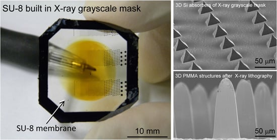
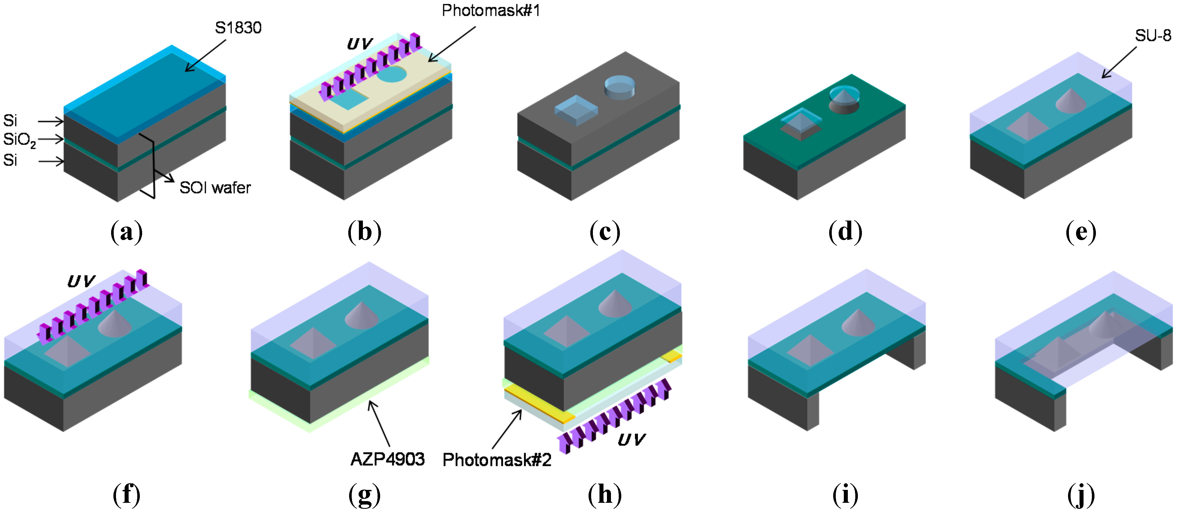
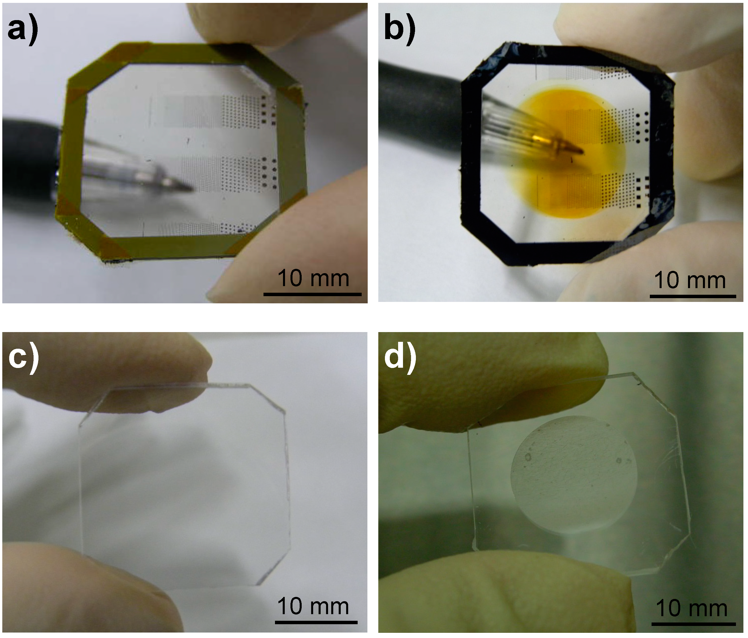
2.1. SU-8 Built-In X-Ray Mask

When designing an X-ray mask, it is necessary to understand the environment in which it is going to be used. An X-ray lithography experiment was carried out at the TERAS [34] SR facility of the National Institute of Advanced Industrial Science and Technology (AIST). Figure 1 shows a calculation result of the output beam spectrum of a beamline BL-4 [35], and of the transmittance of a membrane and of an absorber in a designed X-ray mask. The membrane is made of a 30-μm-thick SU-8, and the absorber consists of a Si film with a maximum thickness of 25 μm and an additional 5-μm-thick SU-8. The spectrum was read of the output beam that was transmitted through a 50-μm-thick Be window and then allowing the beam to pass through a 70-mm long passage of a flowing stream of the He gas (pressure: 1 atm). The beam was generated by an SR that comprised a 10-m-curvature-radius-bending magnet inserted into an electron storage ring of TERAS facility. The optical arrangement of the beamline BL-4 is mentioned later in this paper. In the output beam from the beamline BL-4, when photon energy nears 2 keV, a photon flux appears and serves as a peak. The transmittance of the SU-8 membrane at 2 keV is approximately 30%, and the X-ray hardly penetrates the Si absorber (SU-8 of 5-μm thickness being included). Moreover, at near 4 keV, the transmittance of SU-8 membrane is 75%, and the value of the absorber is only 5%; and it thus amounts to one-fifteenth of the membrane’s value. At the photon energy of 6 keV, although the difference between membrane and absorber is decreased, the contrast ratio of “membrane:absorber” remains 2:1.
Figure 2 shows a process flow of an X-ray grayscale mask’s manufacturing. A silicon on insulator (SOI) wafer that consists of a 30-μm-thick active Si layer, a 1-μm-thick SiO2 layer, and a 525-μm-thick Si substrate, was prepared, and a 3-μm-thick positive-tone photoresist S1830 (Shipley, Kaysville, UT, USA) was spin-coated on the active Si layer (Figure 2a). Cr patterns on a quartz reticle were then transferred to the S1830 photoresist by a UV stepper 1500 MVS R-PC system (Ultratech, San Jose, CA, USA). And the resist was then developed (Figure 2b,c). After the development, there appeared a circular dotted pattern 50 μm in diameter and a square dotted pattern 50 μm in width. Those patterns then served as a masking layer for the next step where the active Si was tapered-trench-etched using a reactive-ion-etching (RIE) system Alcatel 601E system (Alcatel Vacuum Technology, Annecy, France) (Figure 2d). In a tapered-trench-etching technique, an inductively coupled plasma (ICP) source has been used, and the shape of the Si absorbers was controlled by a mixed gas pressure with SF6, C4F8, and O2 gas, and by the etching time. The optimization conditions have been described in References [21,22]. In this experiment, the mixed gas pressure and the etching time were more than 10 Pa and 11 min, respectively.
Figure 1. Calculated output beam spectrum of beamline BL-4 at TERAS synchrotron radiation facility and transmittance of SU-8 membrane (30 μm thickness) and Si (25 μm thickness) absorber on SU-8 film (5 μm thickness) depended on photon energy. “t” in graph legend in the figure means thickness.
Micromachines 06 00252 g001
Figure 2. Process flow to fabricate X-ray mask composed with SU-8 membrane and Si absorber for grayscale lithography. Illustrations show the cross-sectional structure of the X-ray grayscale mask. (a) 1st spin-coating, (b) 1st UV exposure, (c) 1st development, (d) taper-RIE of Si, (e) removal of photoresist and 2nd spin-coating, (f) 2nd UV exposure and post-baking, (g) 3rd spin-coating, (h) 3rd UV exposure, (i) 2nd development and deep RIE of Si, (j) RIE of SiO2.
Micromachines 06 00252 g002
Figure 3a,b show the scanning-electron-microscope (SEM) images of cone- and pyramid-shaped Si structures before the removal of the photoresist layer. The sidewall of the Si structures under the masking layer was inclined, and it can be confirmed that the tapered-trench-etching was successful. Figure 3c,d show Si absorbers after the masking layer being removed. The tips of cone- and pyramid-shaped Si structures appeared sharp and firm, and it was checked that shape of the fabricated tip was sharp. After the remaining S1830 masking layer was removed by acetone, the Si structures on the SiO2 layer were covered by a spin-coated 30-μm-thick SU-8 25 photoresist (MicroChem) (Figure 2e). While keeping a sufficient relaxation time to ease an internal stress, a pre-baking at 95 °C for 10 min, UV irradiation for 1 min using a contact aligner PEM-800 (Union Optical, Tokyo, Japan), a post-baking at 95 °C for 10 min, and another relaxation over night were performed (Figure 2f). After the spin-coating of a 16-μm-thick photoresist AZ4903 (AZ Electronic Materials, Luxembourg, Luxembourg) on the backside of the SOI wafer (Figure 2g), a frame pattern was transferred to AZP4903 photoresist by the same contact aligner (Figure 2h). By a deep RIE using the AZP4903 masking layer and an RIE system MUC-2 (Sumitomo Precision Products, Amagasaki, Japan), the 525-μm-thick Si substrate was etched completely (Figure 2i), and the SiO2 layer was also successfully etched using another RIE system Model RIE-10NRS (Samco, Kyoto, Japan) without breaking the SU-8 membrane (Figure 2j). In the final step, the masking layer that remained on the Si frame was removed by O2 plasma ashing, and an X-ray grayscale mask was thus completed. The details on the process conditions are summarized in Table 2. Figure 4a shows a photograph of the completed X-ray grayscale mask. The square-shaped X-ray mask of 25 mm2 area is surrounded by a 3-μm-wide Si frame. From this photograph, it was checked that the SU-8 membrane has good transmittance in the visible-light region.
Figure 3. Scanning-electron-microscope (SEM) images of 3-dimensional Si absorbers before (a) cone-shaped and (b) pyramid-shaped; and after (c) cone-shaped and (d) pyramid-shaped the removal of S1830 photoresist.
Micromachines 06 00252 g003
Figure 4. Photographs of X-ray mask (a) before; and (b) after X-ray irradiation; and of PMMA sheet (c) before; and (d) after X-ray exposure and development.
Micromachines 06 00252 g004
Table 2. Process conditions to fabricate X-ray mask.
ProcessMaterialParameterCondition
1st Spin-coatingS1830thickness3 μm
1st UV exposuretime15 s
Pre-bakingtemperature120 °C
time20 min
1st DevelopmentNF-319temperatureRoom Temperature
time5 min
Tapered trench etchinggasSF6 + C4F8 + O2
pressure3.7–9.5 Pa
time11 s
Removal (+Ultrasonic)Acetonetime10 min
2nd Spin-coatingSU-8 25thickness30 μm
Pre-bakingtemperature95 °C
time10 min
2nd UV exposuretime1 min
Post-bakingtemperature95 °C
time10 min
3rd Spin-coatingAZP4903thickness16 μm
3rd UV exposuretime35 s
2nd DevelopmentAZ400k + Distilled water (1:3)temperatureRoom Temperature
time5 min
Deep RIE of SigasSF6 + C4F8
time150 min
RIE of SiO2gasCHF3
time50 min
AshinggasO2
time10 min

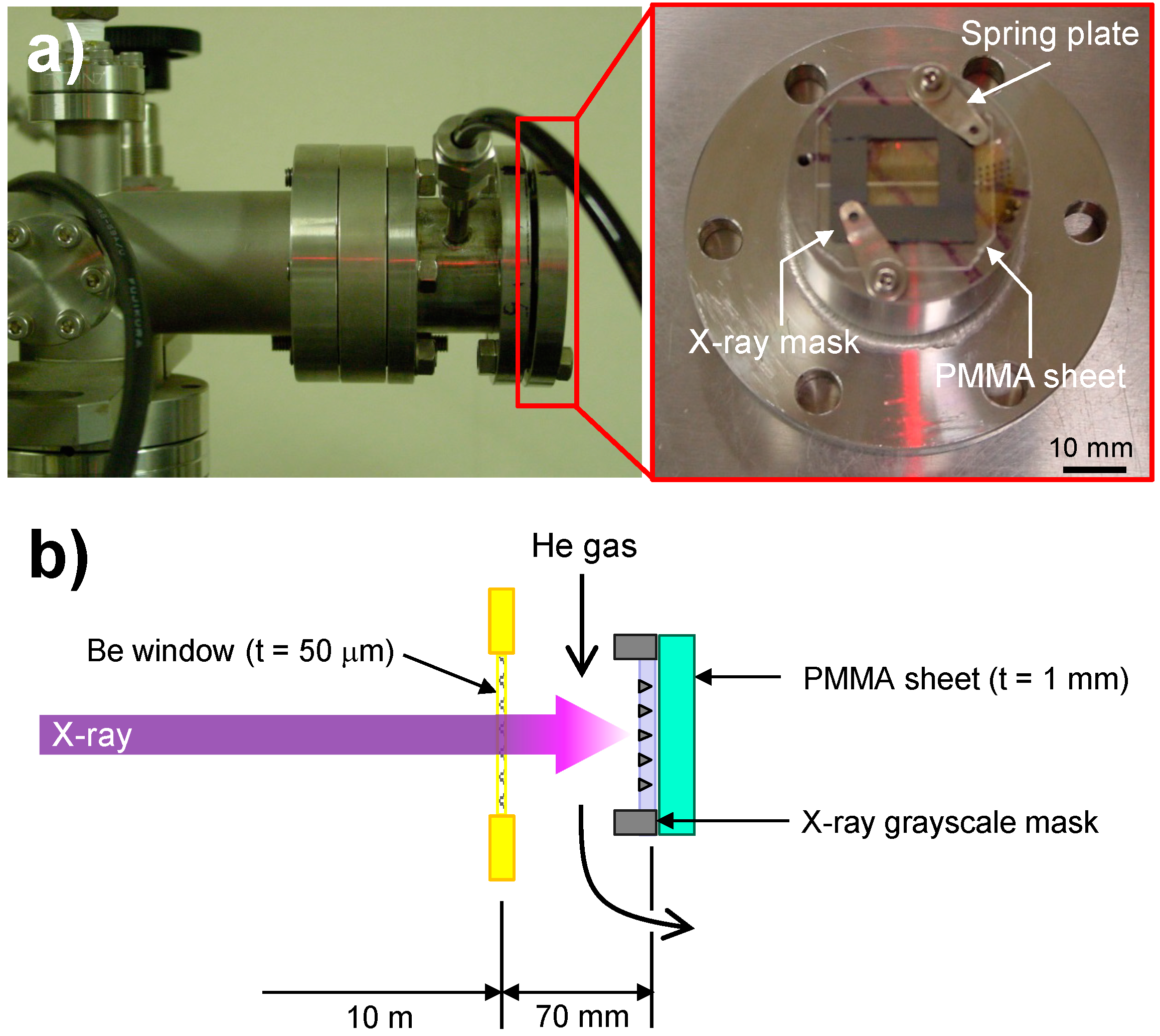
2.2. X-Ray Exposure and Development

Figure 5 shows an end station of the beamline BL-4. In this experiment, 1-mm-thick PMMA sheet was chosen as a photoresist for X-ray lithography. Figure 4c shows a PMMA sheet before the X-ray exposure. In keeping up with the requirements of an X-ray grayscale mask’s size, the four corners of a 25-μm-square PMMA sheet were cut out. As shown in the right half of Figure 5a, the X-ray grayscale mask and the PMMA sheet were fixed on an exposure stage by two spring-loaded plates so that the SU-8 membrane could make contact with the surface of the PMMA sheet. The exposure stage with a diameter of 70 mm was inserted at the end of the beamline BL-4.
Figure 5b shows an optical arrangement of the beamline BL-4. The synchrotron radiation, which was generated from the bending magnet is led to an exposure chamber through a Be window with a thickness of 50 μm arranged at a distance of 10 m from the bending magnet. In an exposure chamber, the air was replaced by a flowing stream of He gas through the chamber, and the exposure stage was set from the Be window at a distance of 70 mm. The X-ray exposure energy was estimated and controlled as a dose energy (mA·h), which is a product of a storage ring current and X-ray irradiation time. At the TERAS SR facility, after an electron is accelerated to 750 MeV and accumulated until the storage ring current reaches to 270 mA, it is then reduced to 50 mA during an operation for a day. The X-ray irradiation experiment was conducted over several days using the system to its full capacity during its operation time of 5–6 h, a day. The PMMA sheet used after the X-ray exposure, was developed by a GG developer consisting of diethyleneglycol-monobutylether (60 vol %), morpholin (20 vol %), ethanol-amine (5 vol %) at 25 °C for 18 h, and distilled water (15 vol %); and then was washed by a distilled water. The PMMA sheet after the X-ray exposure and development is shown in Figure 4d. The irradiated area by the X-rays can be clearly observed as a 15-mm-diameter circle. In the next step, the completed PMMA structure and the X-ray mask, after the X-ray irradiation was evaluated using SEM and an optical microscope.
Figure 5. (a) Photographs of the end station of the beamline BL-4 (left) and exposure stage (right); (b) Cross-sectional schematic view of the end station of the beamline BL-4 during the X-ray exposure.
Micromachines 06 00252 g005

3. Results and Discussion

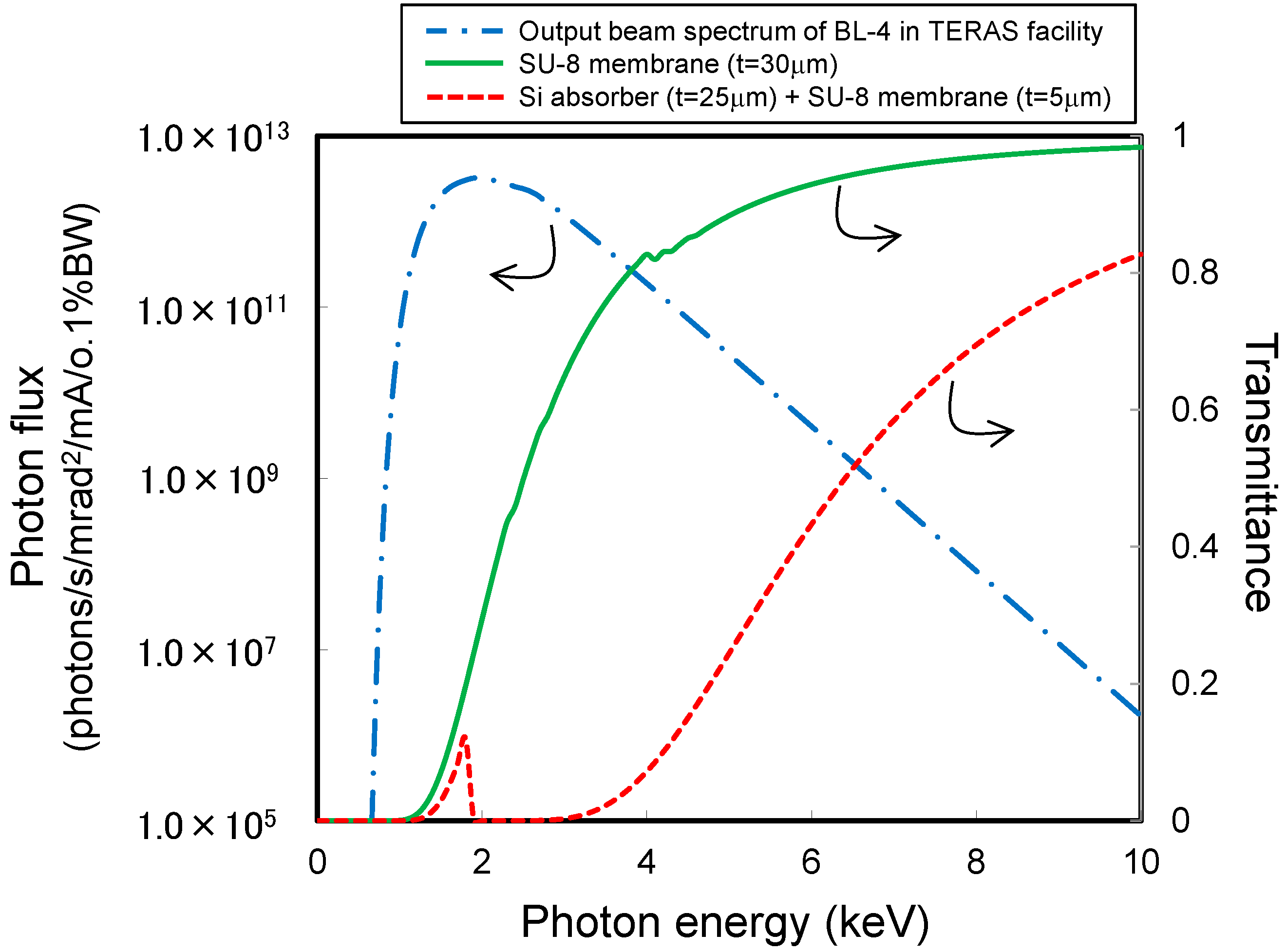
3.1. Transmission Property of SU-8 in the X-Ray Energy Region

The exposure depths on the PMMA by the output beam from the beamline BL-4 in both cases of the absence and presence of the 30-μm-thick SU-8 membrane are compared in Figure 6. A curved line in the figure indicates an approximation. The difference between both cases lies in their maximum values when the dose energy is 100 mA·h. The exposure depth in the absence and presence of the SU-8 membrane was measured as 70 and 35 μm, respectively; and specifically the ratio was estimated as 2:1. As shown in Figure 1, in the photon energy range of 2–6 keV, the transmittance of SU-8 of 30-μm thickness increases gradually from 20% to 95%. Because a peak of the photon flux of the output beam from the beamline BL-4 shows up at near 2 keV and the transmittance of SU-8 at near 2 keV is 40% and more, the result, that the exposure depth in the presence of the SU-8 membrane is roughly half compared to the value in the absence of the SU-8 membrane, is quite understandable.
Figure 6. Exposure depth of PMMA sheet in cases of the absence and presence of the SU-8 membrane depended on the dose energy.
Micromachines 06 00252 g006

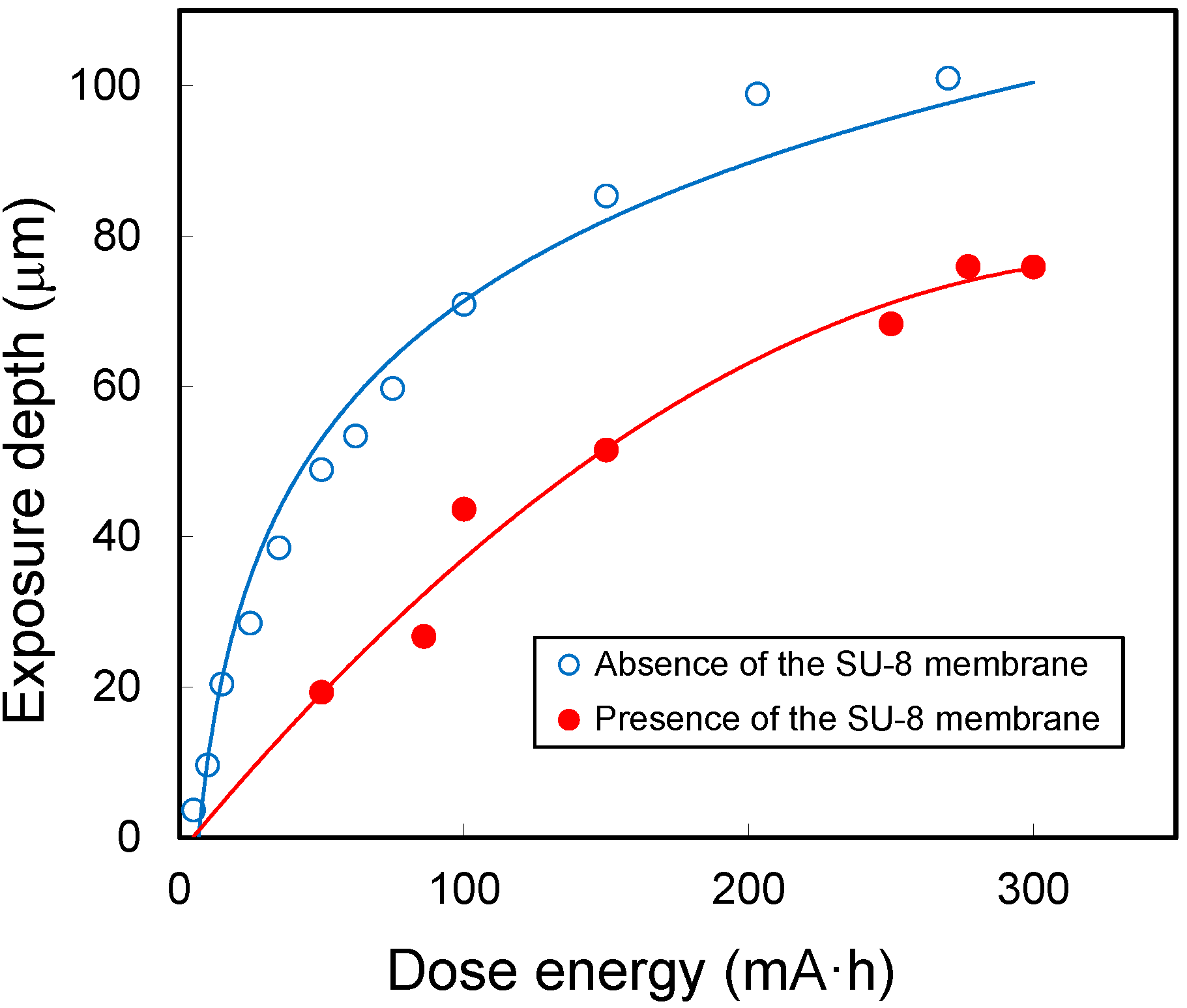
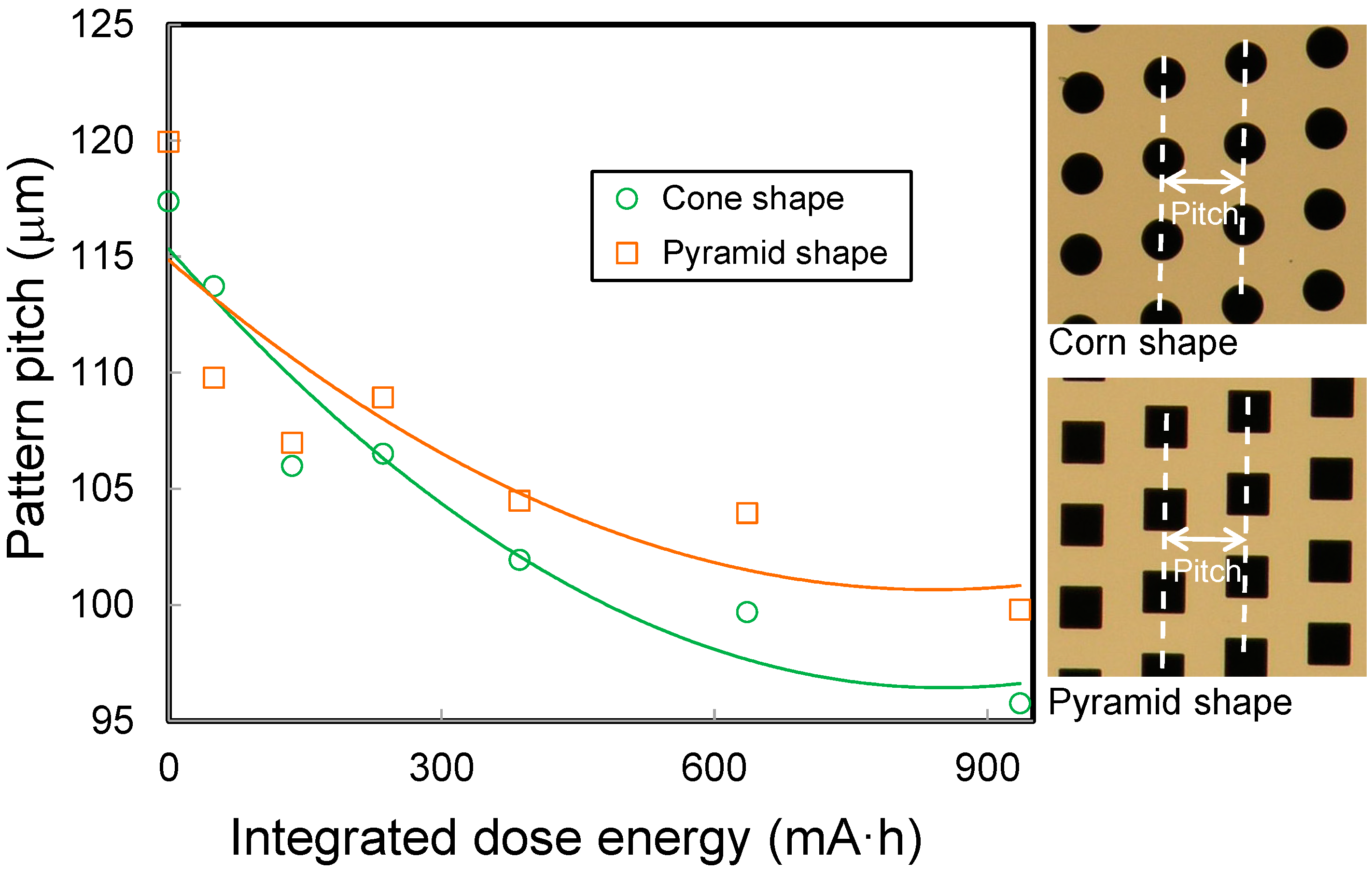
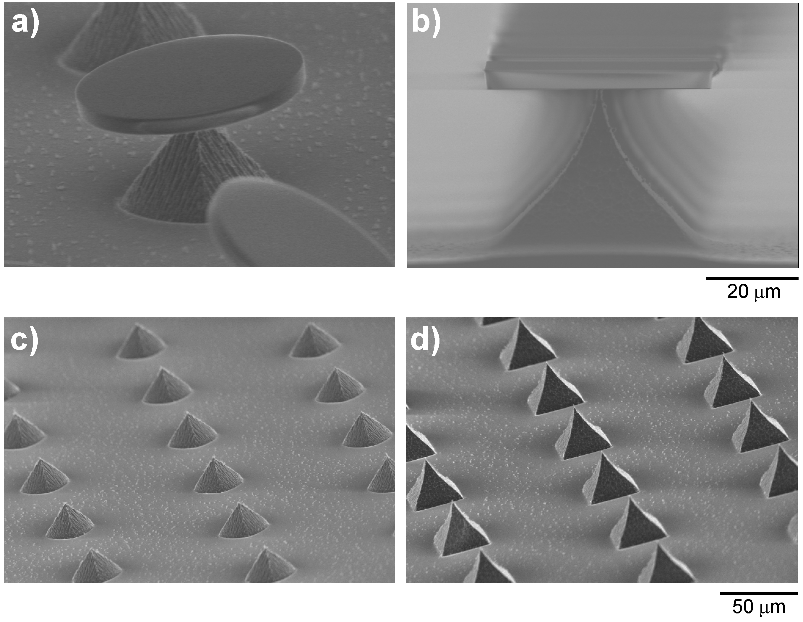
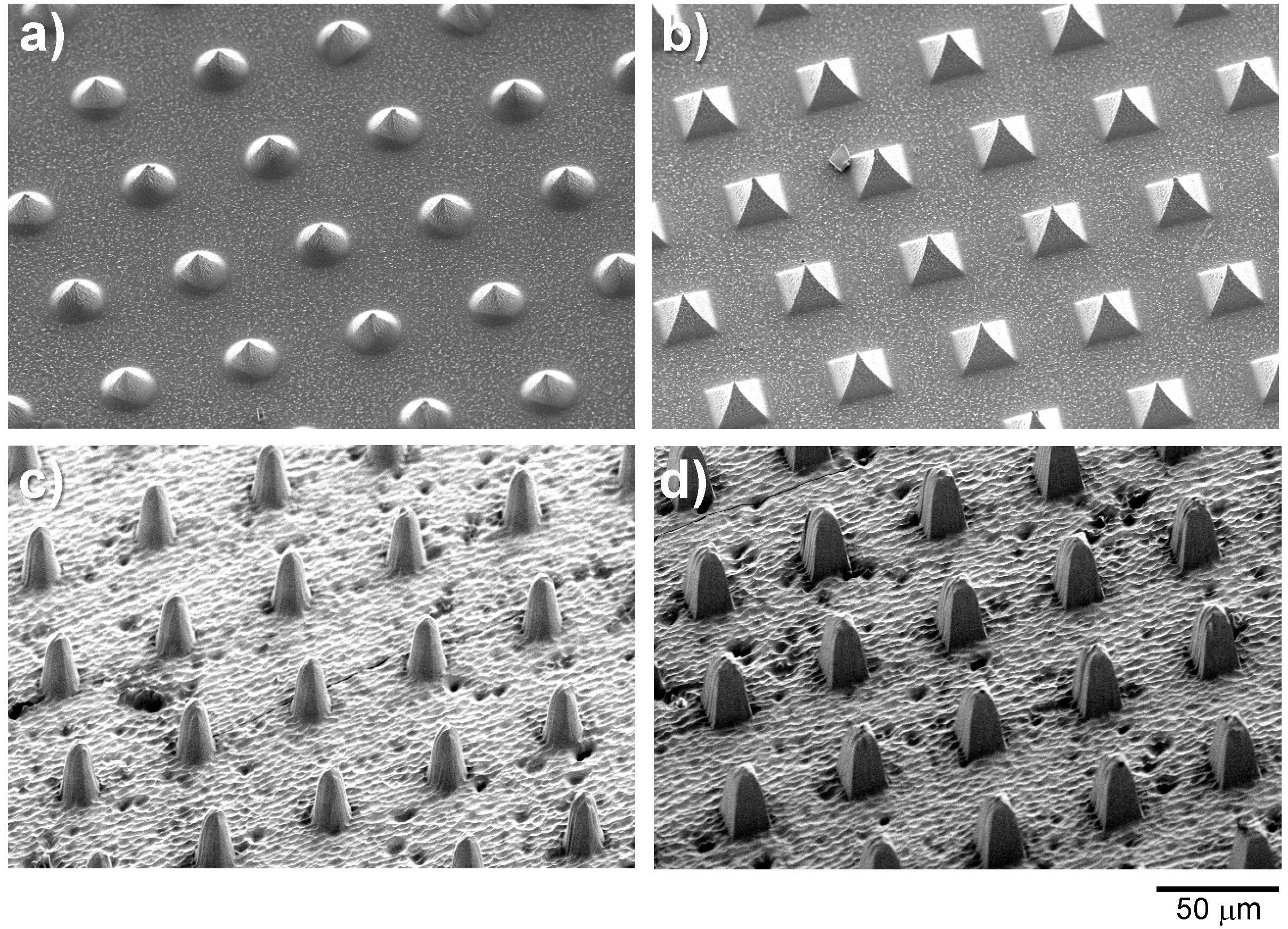
3.2. Transition of Pattern Width with SU-8 Thermal Expansion

Since the 1-mm-thick PMMA sheet was hard, the PMMA sheet after X-ray lithography was put into liquid nitrogen, and then cleaved by hand. And then in order to prevent any charge built-up, a 10-nm-thick Pt was sputter-deposited on the sample surface before an SEM observation was made. The left and right halves of Figure 7 are the results of pattern transferring from cone- and pyramid-shaped Si absorbers to a PMMA structure, respectively. As for the exposure conditions, in the upper figures, the dose energy was set at 50 mA (Figure 7a,b); another case of a 300-mA dose energy is shown in the lower figures (Figure 7c,d).
From these SEM images, it is confirmed that the X-ray grayscale mask has a sufficient contrast between the absorber and membrane. As shown in Figure 3, a cone-shaped Si absorber was 46 μm in diameter and 27 μm in height; and a pyramid-shaped Si absorber was 42 μm in the bottom width and 27 μm in height. Figure 7 shows a transition of pattern widths on the PMMA sheets exposed by the various dose energies. Although the 50-μm-diameter circular and 50-μm-wide square dotted patterns were accurately transferred from the photomask to the photoresist, at the early step of fabricating the X-ray grayscale mask, a pattern size reduction of 8%–16% was made by the tapered-trench-etching. After that, cone- and pyramid-shaped Si absorbers were transferred by deep X-ray lithography to PMMA structures of 34.5 μm in diameter, and 36.2 μm in width on average. In this process, the pattern width decreased further down to 75%–86% of Si absorbers.
This pattern width reduction originates from the diffraction effect in which case the X-rays bending around the edges and reaching to the backside of Si absorbers occurs. Usually, in the area where the X-rays were irradiated, a certain degree of heating took place and the absorber, and the membrane expanded depending on their coefficients of thermal expansion. In the beamline BL-4, infrared rays are significantly cut by the Be window; and a device was equipped to cool the exposure stage continuously by a flowing stream of the He gas. However, a certain degree of thermal expansion is unavoidable, and a degradation of the pattern transfer accuracy does occur, and remains as a matter of concern. While the X-ray grayscale mask is irradiated with X-rays, the irradiated area gradually reaches to a high temperature, and the membrane also expands. Therefore, according to the expansion of the membrane, the pattern’s position is shifted because the isolated Si absorbers were embedded within the SU-8 membrane. As shown in Figure 8, the bottom width of the PMMA structures does not exceed the width of the Si absorbers; it rather shrinks to a smaller dimension as dictated by the diffraction effect of the X-rays. This result is the proof, which was about maintaining a very stable accuracy of position, without the expanding of the SU-8 membrane during the X-ray irradiation.
Figure 7. Cross-sectional SEM images of the PMMA structures, which (a,c) cone and (b,d) pyramid shapes of Si absorber were transferred by the X-rays at dose energies of 50 and 300 mA, respectively.
Micromachines 06 00252 g007
Figure 8. Bottom width of the PMMA structures fabricated by X-rays which penetrated through the cone and pyramid shaped structures of the Si absorbers depended on the dose energy.
Micromachines 06 00252 g008

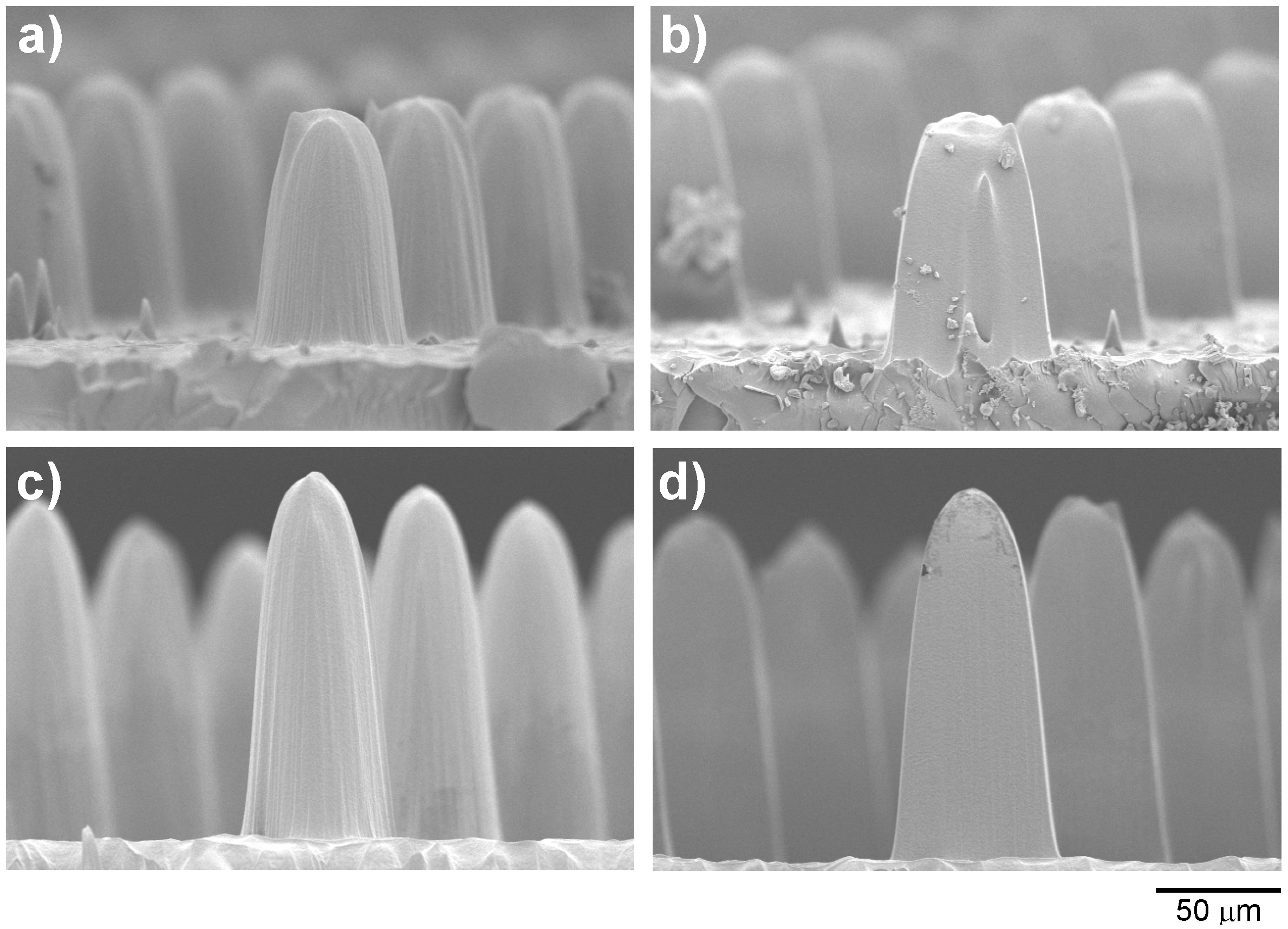
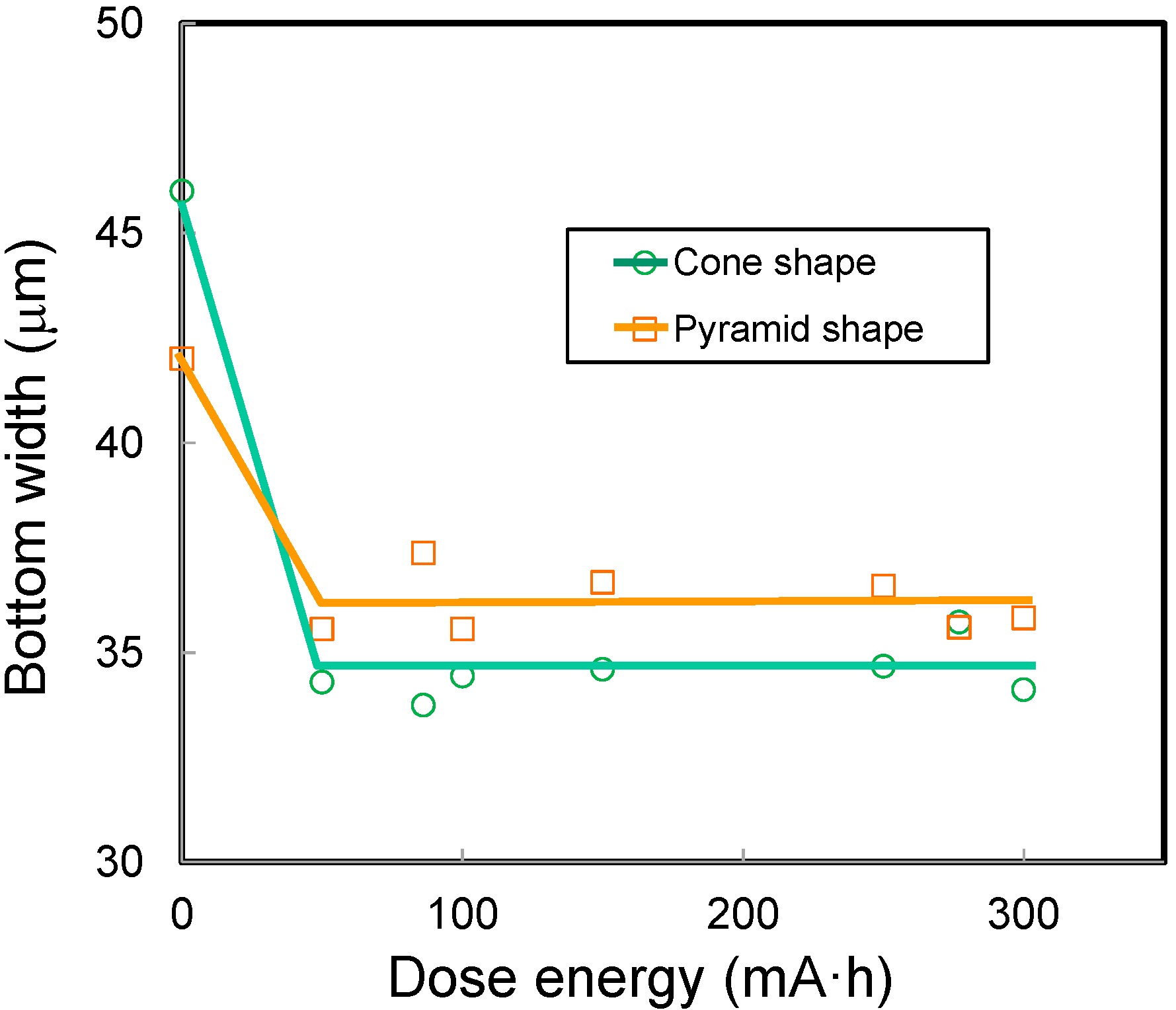
3.3. Tolerance of SU-8 to Synchrotron Radiation

Figure 9 shows the SEM images of the Si absorbers on the X-ray grayscale mask and the PMMA structures after X-ray lithography. Using these top view images, a pitch between the structures was measured. The investigation result of the durability of the grayscale mask to X-rays is shown in Figure 10. In the figure, the average values of both patterns’ pitches in X and Y directions (Px and Py) are plotted, and the data has been approximated and represented in form of two curves. In the X-ray mask manufacturing step, the SU-8 spin-coated on the SiO2 layer was baked twice, and an internal stress was accumulated in a relatively soft SU-8. The coefficients of the thermal expansion of SU-8 (52 × 10−6/K) [28,29] and SiO2 (0.7 × 10⁻⁶/K) [36] are quite different from each other. When the SiO2 film was removed by the RIE as a post process, the internal stress of the SU-8 was eased, resulting in them being expanded, and in the bending of the SU-8 membrane. As a result, the circular and square dotted patterns, which were of 100-μm pitches on the photomask, are spread to 120 and 117 μm, respectively.
Figure 9. SEM images of the Si absorbers on the X-ray grayscale mask before spin-coating of SU-8: (a) cone and (b) pyramid shape. SEM images of the PMMA microstructures fabricated by X-ray lithography at the dose energy of 300 mA·h; (c) cone and (d) pyramid shape. Reprinted with permission from [22].
Micromachines 06 00252 g009
Figure 10. Pattern pitch of PMMA structures which cone, and pyramid shapes of Si absorbers was transferred by X-rays depended on the integrated dose energy. Pitches in X and Y directions indicated as Px and Py in the figure, respectively.
Micromachines 06 00252 g010

4. Conclusions

The performance of an X-ray grayscale mask that consisted of Si absorbers processed by tapered-trench-etching, and of a SU-8 membrane was evaluated using a beamline BL-4 of TERAS SR facility at AIST. Three kinds of characteristic are required of a membrane material for X-ray lithography. The first is a transmission property of X-rays. When a 30-μm-thick SU-8 membrane was absent or present, an exposure depth of a PMMA photoresist was measured and was compared with a calculated transmittance of SU-8 in an X-ray energy region. In fact, the measured value and the calculated value were well in agreement. Next, it is important that a pattern width does not change with a membrane’s thermal expansion during the X-ray irradiation. This transition leads to a fatal defect in grayscale lithography. On a positive note, it was learned that a displacement of the pattern width at different dose energies was controllable within 2 μm. Finally, it remains to be addressed if SU-8 has plenty of tolerance to synchrotron radiation. If an operating time of the X-ray mask is increased, the polymerization by cross-linking in the SU-8 film was moved forward and a solvent that remains inside the SU-8 membrane can evaporate and the membrane could become brittle. Although the membrane’s color would also be changed, a reduction of a pattern pitch was found to be saturated when the integrated dose energy reached to 900 mA·h. Moreover, the measured pitch became almost equal to the designed value. These results proved that the X-ray grayscale mask with the SU-8 membrane does perform well for all practicality and can be used in an X-ray mask after a suitable baking process by irradiation of X-rays. It is also believed that with this method, the pattern transfer quality can be achieved to be very high.

Acknowledgments

X-ray exposure experiments were executed using the SR Facility TERAS of the National Institute of Advanced Industrial Science and Technology (AIST). The authors would like to thank Koichi Awazu of Electronics and Photonics Research Institute, and to the Quantum Radiation Research group at the Research Institute of Instrumentation Frontier in AIST. The author accepted technical supports in Si taper-trench-etching from Takayuki Takano of the Advanced Manufacturing Research Institute in AIST (at the time).

Conflicts of Interest

The author declares no conflict of interest.

References and Notes

  1. Wu, B.; Kumar, A. Extreme ultraviolet lithography: A review. J. Vac. Sci. Technol. B 2007, 25, 1743–1761. [Google Scholar] [CrossRef]
  2. Kinoshita, H.; Wood, O. An Historical Perspective. In EUV Lithography; Bakshi, V., Ed.; SPIE Press: Bellingham, WA, USA, 2007; pp. 1–54. [Google Scholar]
  3. Malek, C.K.; Saile, V. Applications of LIGA technology to precision manufacturing of high-aspect-ratio micro-components and systems: A review. Microelectron. J. 2004, 35, 131–143. [Google Scholar] [CrossRef]
  4. Salker, V. Introduction: LIGA and Its Applications. In LIGA and Its Applications; Saile, V., Wallrabe, U., Tabata, O., Korvink, J.G., Eds.; Wiley-Vch: Weinheim, Germany, 2009; pp. 1–10. [Google Scholar]
  5. Becker, E.W.; Ehrfeld, W.; Hagmann, P.; Manwe, A.; Münchmeyer, D. Fabrication of microstructures with high aspect ratios and great structural heights by synchrotron radiation lithography, galvanoforming, and plastic moulding (LIGA process). Microelectron. Eng. 1986, 4, 35–56. [Google Scholar] [CrossRef]
  6. Bogdanov, A.L.; Peredlkov, S.S. Use of SU-8 photoresist for very high aspect ratio X-ray lithography. Microelectron. Eng. 2000, 53, 493–496. [Google Scholar] [CrossRef]
  7. Desta, Y.; Goettert, J. X-Ray Masks for LIGA Microfabrication. In LIGA and Its Applications; Saile, V., Wallrabe, U., Tabata, O., Korvink, J.G., Eds.; Wiley-Vch: Weinheim, Germany, 2009; pp. 11–50. [Google Scholar]
  8. Utsumi, Y.; Kishimoto, T.; Hattori, T.; Hara, H. Large-area x-ray lithography system for liga process operating in wide energy range of synchrotron radiation. Jpn. J. Appl. Phys. 2005, 44, 5500–5504. [Google Scholar] [CrossRef]
  9. Mekaru, H.; Takano, T.; Ukita, Y.; Utsumi, Y.; Takahashi, M. A Si stencil mask for deep X-ray lithography fabricated by MEMS technology. Microsyst. Technol. 2008, 14, 1335–1342. [Google Scholar] [CrossRef]
  10. Flanders, D.C.; Smith, I. Polyimide membrane X-ray lithography masks—Fabrication and distortion measurements. J. Vac. Sci. Technol. 1978, 15, 995–997. [Google Scholar] [CrossRef]
  11. Spiller, E.; Feder, R.; Topalian, J.; Castellani, E.; Romankiw, L.; Heritage, M. X-ray lithography for bubble devices. Solid State Technol. 1979, 19, 62–68. [Google Scholar]
  12. Lee, S.; Kim, D.; Jin, Y.; Han, Y.; Desta, Y.; Bryant, M.D.; Goettert, J. A Micro corona motor fabricated by a SU-8 built-on X-ray mask. Microsyst. Technol. 2004, 10, 522–526. [Google Scholar] [CrossRef]
  13. Schmidt, C.J.; Lenzo, P.V.; Spencer, E.G. Preparation of thin windows in silicon masks for X-ray lithography. J. Appl. Phys. 1975, 46, 4080–4082. [Google Scholar] [CrossRef]
  14. Watts, R.K. X-ray lithography. Solid State Technol. 1979, 22, 68–82. [Google Scholar]
  15. Bassous, E.; Feder, E.; Spiller, E.; Topalian, J. High transmission X-ray masks for lithographic applications. Proc. Int. Electron Devices Meet. 1975, 21, 17–19. [Google Scholar]
  16. Desta, Y.M.; Aigeldinger, G.; Zanca, K.J.; Coane, P.J.; Goettert, J.; Murphy, M.C. Fabrication of graphite masks for deep and ultradeep X-ray lithography. Proc. Mater. Device Charact. Micromach. III 2000, 4175, 122–130. [Google Scholar]
  17. Hofer, D.; Powers, J.; Grobman, W.D. X-ray lithographic patterning of magnetic bubble circuits with submicron dimensions. J. Vac. Sci. Technol. 1979, 16, 1968–1972. [Google Scholar] [CrossRef]
  18. Yamada, M.; Nakaishi, M.; Kudou, J.; Eshita, T.; Furumura, Y. An X-ray mask using Ta and heteroepitaxially grown SiC. Microelectron. Eng. 1989, 9, 135–138. [Google Scholar] [CrossRef]
  19. Lüthje, H.; Harms, H.; Matthiessen, B.; Bruns, A. X-ray lithography: Novel fabrication process for SiC/W steppermasks. Jpn. J. Appl. Phys. 1989, 28, 2342–2347. [Google Scholar] [CrossRef]
  20. Iba, Y.; Kumasaka, F.; Iizuka, T.; Yamabe, M. Amorphous refractory compound film material for X-ray mask absorbers. Jpn. J. Appl. Phys. 2000, 39, 5329–5333. [Google Scholar] [CrossRef]
  21. Mekaru, H.; Takano, T.; Awazu, K.; Takahashi, M.; Maeda, R. Fabrication and evaluation of a grayscale mask for X-ray lithography using MEMS technology. J. Micro/Nanolithogr. MEMS MOEMS 2008, 7, 013009. [Google Scholar] [CrossRef]
  22. Mekaru, H.; Takano, T.; Awazu, K.; Takahashi, M.; Maeda, R. Fabrication of a needle array using a Si gray mask for X-ray lithography. J. Vac. Sci. Technol. B 2007, 25, 2196–2201. [Google Scholar] [CrossRef]
  23. Mekaru, H.; Takano, T.; Awazu, K.; Takahashi, M.; Maeda, R. Demonstration of fabricating a needle array by the combination of X-ray grayscale mask with the lithografie, galvanoformung, abformung process. J. Micro/Nanolithogr. MEMS MOEMS 2009, 8, 033010. [Google Scholar] [CrossRef]
  24. Kudryashov, V.; Yuan, X.; Cheong, W.; Radhakrishnan, K. Grey scale structures formation in SU-8 with e-beam and UV. Microelectron. Eng. 2003, 67–68, 306–311. [Google Scholar] [CrossRef]
  25. Watt, F. Focused high energy proton beam micromachining: A perspective view. Nucl. Instrum. Methods Phys. Res. B 1999, 158, 165–172. [Google Scholar] [CrossRef]
  26. DuPontTM Kapton® HN, Polyimide Film. Available online: http://www.dupont.com/content/dam/assets/products-and-services/membranes-films/assets/DEC-Kapton-HN-datasheet.pdf (accessed on 5 February 2015).
  27. Product Information, Mular®, Polyester Film. Available online: http://usa.dupontteijinfilms.com/informationcenter/downloads/Physical_And_Thermal_Properties.pdf (accessed on 5 February 2015).
  28. Del Campo, A.; Greiner, C. SU-8: Aphotoresist for high-aspect-ratio and 3D submicron lithography. J. Micromech. Microeng. 2007, 17, R81–R95. [Google Scholar] [CrossRef]
  29. Lorenz, H.; Laudon, M.; Renaud, P. Mechanical characterization of a new high-aspect-ratio near UV-photoresist. Microelectron. Eng. 1998, 41, 371–374. [Google Scholar] [CrossRef]
  30. Okada, Y.; Tokumura, Y. Precise determination of lattice parameter and thermal expansion coefficient of silicon between 300 and 1500 K. J. Appl. Phys. 1984, 56, 314–320. [Google Scholar] [CrossRef]
  31. Tien, C.; Lin, T. Thermal expansion coefficient and thermomechanical properties of SiNx thin films prepared by plasma-enhanced chemical vapor deposition. Appl. Opt. 2012, 51, 7229–7235. [Google Scholar] [CrossRef] [PubMed]
  32. Goldberg, Y.; Levinshtein, M.E.; Rumyantsev, S.L. Chapter 5: Silicon Carbide (SiC). In Properties of Advanced Semiconductor Materials: GaN, AlN, InN, BN, SiC, SiGe; Levinshtein, M.E., Rumyantsev, S.L., Shur, M.S., Eds.; John Wiley & Sons: Hoboken, NJ, USA, 2001; pp. 93–148. [Google Scholar]
  33. The coefficient of thermal expansion on graphite was applied by Tokai Carbon Co., Ltd. (Tokyo, Japan)
  34. Toyokawa, H.; Awazu, K.; Hohara, S.; Koike, M.; Kuroda, R.; Morishita, Y.; Saito, N.; Saito, T.; Tanaka, M.; Watanabe, K.; et al. Present status of the electron storage ring TERAS of AIST. In Proceedings of the First Annual Meeting of Particle Accelerator Society of Japan and the 29th Linear Accelerator Meeting in Japan, Funabashi, Japan, 4–6 August 2004; pp. 203–205.
  35. Awazu, K.; Wang, X.; Fujimaki, M.; Kuriyama, T.; Sai, A.; Ohki, Y.; Imai, H. Fabrication of two- and three-dimensional photonic cystals of titania with submicrometer resolution by deep X-ray lithography. J. Vac. Sci. Technol. B 2005, 23, 934–939. [Google Scholar] [CrossRef]
  36. Tada, H.; Kumpel, A.E.; Lathrop, R.E.; Stanina, J.B.; Nieva, P.; Zavracky, P.; Miaoulis, I.N.; Wong, P.Y. Thermal expansion coefficient of polysrystalline silicon and silicon dioxide thin films at high temperatures. J. Appl. Phys. 2000, 87, 4189–4193. [Google Scholar] [CrossRef]

