1. Introduction
Ever since its first introduction [
1], the epoxy-based negative-tone resist SU-8 has drawn a great deal of attention from the micro-fabrication community. The primary reasons for this popularity are the fact that SU-8 shows stable mechanical, thermal and chemical characteristics [
2] and it can be coated in thicknesses greater than 1 mm [
3] and patterned to make tall microstructures with high aspect ratios [
4] which are clearly unprecedented characteristics in conventional photoresists. Utilizing such unique characteristics, cross-linked SU-8 has been used as a sacrificial micro-mold for electroplating as well as final microstructures in a broad filed of applications including micro gears [
5], micro cantilever for scanning force microscopy [
6], microfluidic channel [
7], optical waveguide [
8], and neural probe [
9], to name a few.
Many lithography techniques, such as conventional ultraviolet (UV) lithography [
1], deep X-ray lithography [
10], electron-beam lithography [
11], and proton beam writing [
12] have been utilized to create various tall and high aspect ratio microstructures as well as deep sub-micron scale structures in SU-8. Regardless of the specific types of photoresists and lithography techniques used, typically photoresist is coated on a substrate (e.g., silicon) and high energy beam (e.g., UV, e-beam) is irradiated directly normal to the top surface of the coated photoresist, a so-called front-side exposure. For conventional photoresists which essentially yield very thin (a few microns) planar two-dimensional (2D) structures, variation of lithography techniques is extremely rare because such a variation will not bring much benefit to yield any useful patterned structures much different from that of the front-side exposure. However, there have been numerous unconventional tweaks in SU-8 lithography techniques to create a variety of deep sub-micron structures as well as unique three-dimensional (3D) structures by fully utilizing its tall high-aspect-ratio microstructures capability.
In this review paper, those unique unconventional SU-8 lithography techniques such as inclined UV exposure, back-side UV exposure, drawing lithography, and holographic interference lithography developed over the past two decades and their applications are discussed.
2. Inclined UV Exposure
The first pioneering unconventional UV lithography might be demonstration of thick 3D multi-directional inclined microstructures by Beuret
et al. [
13]. This work used two layers of positive photoresists (AZ 4562) and two slighltly shifted metallic layers directly on the photoresist layers as integrated masks. Utilizing modified inclined rotating chuck, 60–120 μm thick microstructures with inclined angle of approximately 10° were demonstrated both in photoresist and electroplated metal. The inclined exposure along with moving mask exposure were utilized in deep X-ray lithography to create poly(methyl methacrylate) 3-facet micro mirror [
14]. Although it is not an inclined exposure, another work worth commenting is a magentic switch fabricated on a 3D micro-ramp [
15]. Choi
et al. developed the fabrication process to dispense SU-8 photoresist using a syringe on a pre-patterned tilted substrate, and carried out conventional front-side UV exposure on the already inclined SU-8 photoresist to demonstrate 36° inclined angle, 0–300 μm thick continuously varying 3D micro-ramp to realize a magenetically actuated switch.
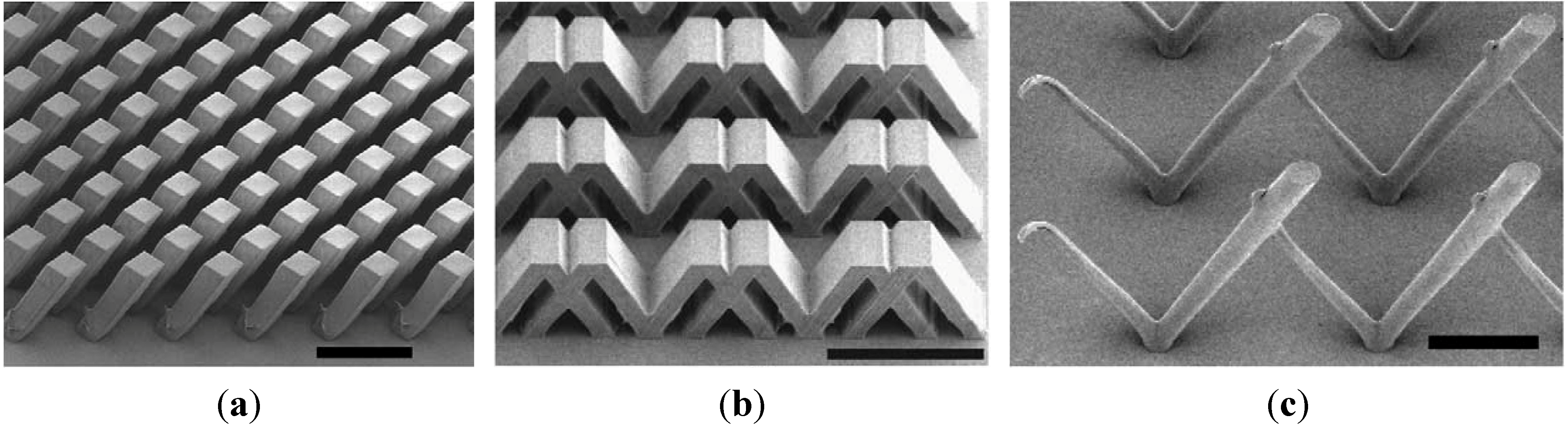
After nearly 10 years of the initial work on the positive photoresist, the inclined exposure technique was applied in SU-8 to realize a variety of unique microstructures. Han
et al. [
16,
17] developed a UV exposure process in which a photomask and a SU-8 coated substrate are in contact and the mask/SU-8 is placed on a inclined/rotated chuck. They demonstrated various 3D microstructures such as oblique angled cylinders, embedded channels, bridges, V-grooves, truncated cones, and so on (
Figure 1). The inclined angle on the SU-8 microstructures turned out to be 19.5° when the incident angle of UV exposure was 32° due to the refractive index difference between the SU-8 and air. Along with single and multiple inclined UV exposure, effect of the reflection of UV at the interface between the coated SU-8 and the substrate was studied. A reflection enhancing layer such as aluminum was intentionally deposited on a substrate and increased UV dose was used to create dual 3D oblique microstructures in the light path in one exposure (
Figure 1c). It is clearly noticeable that the structure formed in the reflected beam is narrower than that of the incident beam because of the reduced UV energy as the UV light is absorbed through the SU-8 layer.
Figure 1.
SEM (scanning electron microscope) images of the (
a) single inclined UV exposure (scale bar 100 μm); (
b) double inclined UV exposure (scale bar 200 μm) and (
c) single inclined exposure with enhanced reflection at the surface (scale bar 100 μm). Reprinted with permission from [
17], copyright 2004 Elsvier.
Since the refractive index (
n) of SU-8 at UV exposure wavelengths is approximately 1.67 [
18], according to the Snell’s law, the maximum inclined angle in SU-8 microstructures using the inclined UV exposure is limited to 36.78° (
). To overcome such a limitation, Hung
et al. suggested an immersion lithography technique (
Figure 2) [
19,
20] using high index glycerol (approximate
n = 1.6 at UV exposure wavelengths). In this approach, they used a photomask directly in contact with the coated SU-8 on a substrate and the mask/SU-8 is immersed in glycerol solution to achieve larger angle inclined microstructures (
Figure 3). Microstructures with inclined angles up to 70.8° were demonstrated along with a demonstration of dual 45° mirror structures in SU-8 with integrated Fresnel lens as a potential application in optical pickup.
An index-matching inclined UV exposre process using a high-index (
n = 1.53) prism was also developed with a combination of index-matching glyceryl (
n = 1.45) [
21]. This inclined exposure process was applied to demosntrate out-of-plane microlenses for on-chp optical microsystem in such a manner that microlenses have optical axis parallel with the substrate. The UV exposure dosage was intentionally reduced to have rounded surface profile on the dual exposed SU-8 microlenses. Various sizes of lens in the range of 150–350 μm and optical characteristics of the microlenses were measured. The microlens showed focal length in the range of 110.3–388 μm with the diameter of the focus pad in the range of 32.1–107.7 μm and the depth of focus was found to be in the range of 41.7–46.2 μm [
22,
23]. The same group also applied the inclined SU-8 exposure technique to demosntrate 3D hydro-focusing micro cell sorter for microfluidic cytometry application [
24].
Figure 2.
Conceptual schematic diagram of the index-matching glycerol-based immersion UV lithography for high inclined angle SU-8 microstructure fabrication. Reprinted with permission from [
20], copyright 2004 Institute of Physics.
Figure 2.
Conceptual schematic diagram of the index-matching glycerol-based immersion UV lithography for high inclined angle SU-8 microstructure fabrication. Reprinted with permission from [
20], copyright 2004 Institute of Physics.
Figure 3.
SEM images of the fabricated inclined SU-8 pillars with various angles. Reprinted with permission from [
20], copyright 2004 Institute of Physics.
Figure 3.
SEM images of the fabricated inclined SU-8 pillars with various angles. Reprinted with permission from [
20], copyright 2004 Institute of Physics.
The inclined SU-8 UV exposure technique was also applied to create 3D micro impellor structures for active mixing in microfluidics by Nallani
et al. [
25]. In this work, 31.6° inclined 3D electrplated nickel-iron (NiFe) ferromagnetic impellors were fabricated using the inclined SU-8 UV exposure (
Figure 4). The effiency of micro-mixing of the 31.6° inclined sidewall impellors and that of the vertical straight sidewall impellors were compared and it was found that the 3D impellor increased the mixing efficiency approximately 20%.
Figure 4.
SEM images of the 31.6° angle inclined (
a) curved and (
b) straight sidewall NiFe ferromagnetic 3D impellors. Reprinted with permision from [
25], copyright 2007 Society of Photo Optical Instrumentation Engineers.
Figure 4.
SEM images of the 31.6° angle inclined (
a) curved and (
b) straight sidewall NiFe ferromagnetic 3D impellors. Reprinted with permision from [
25], copyright 2007 Society of Photo Optical Instrumentation Engineers.
Choi
et al. utilized varying mask dimensions with the inclined UV exposure technique to have varying depths of inverse pyramid microstructures in SU-8. Then, the SU-8 was used as a mold and the inverse pattern was transferred to polydimethylsiloxane (PDMS) two consecutive times. Then, the second PDMS pattern was used as a template and polymer was casted to have nearly identical shape of the inverse image of the original SU-8 microstructures [
26]. With the metal transfer micromolding technique combined in this series of pattern transfer technique, varying height metallized microneedles along with polymer microneedles were demonstrated.
3. Back-Side UV Exposure
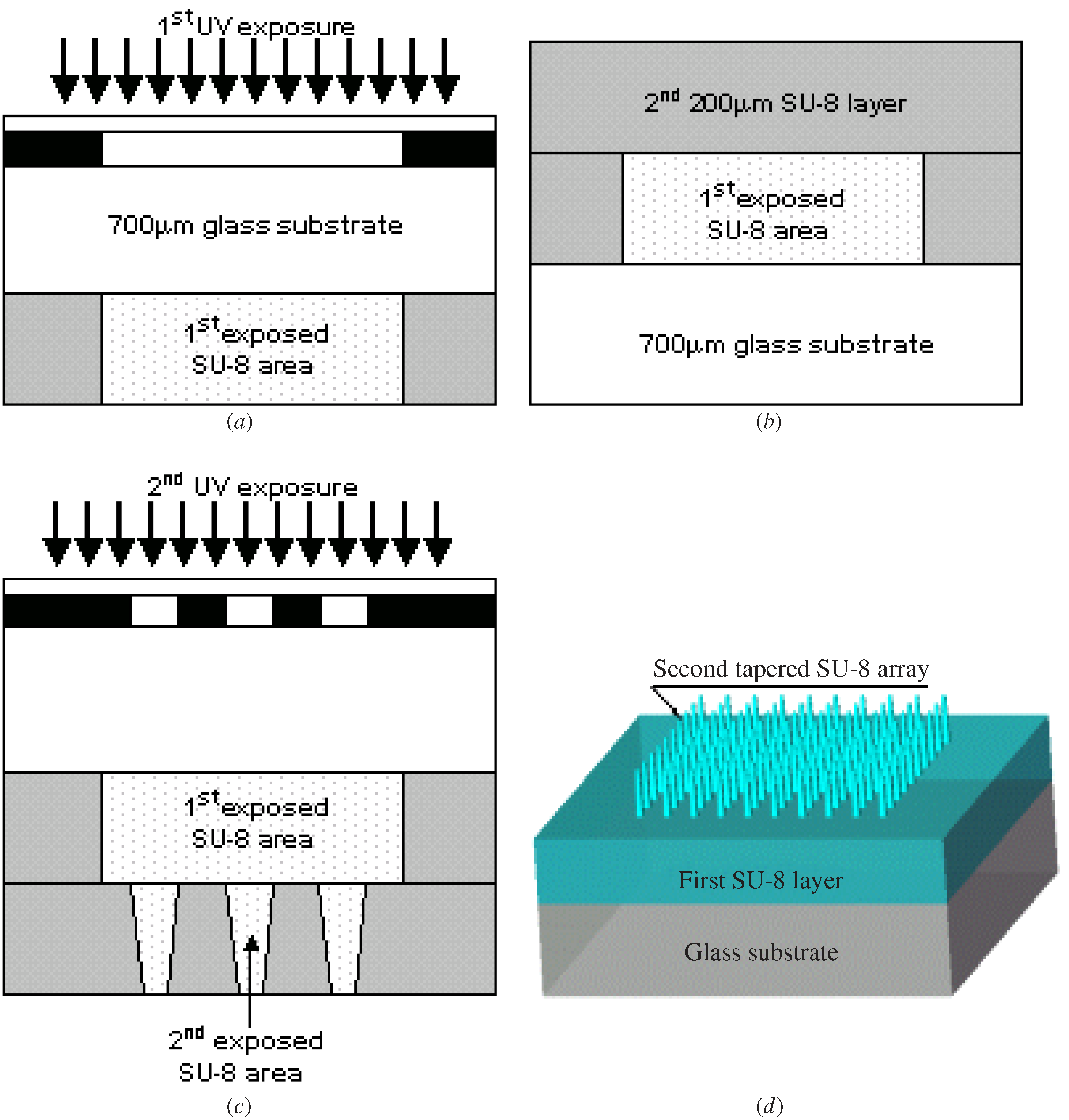
Along with the inclined exposure lithography technique, one of the most common tweaks applied for SU-8 photolithography and found to be useful is back-side exposure. As the photoresist layer gets thicker, UV exposure dose difference between the top and the bottom of the photoresist layer gets larger. Due to this non-uniform UV exposure dose along the photoresist layer, the top layer is over-exposed while the bottom layer is relatively under-exposed. In the case of negative SU-8 photoresist, this will give a microstructure with wider top and narrower bottom. If the exposure takes place from the back-side using SU-8 coated on top of a UV transparent substrate such as glass, structures formed by this back-side exposure will give a relatively wider bottom and narrower top structure.
Kim
et al. reported such a fabrication process which is back-side exposure of SU-8 to create metallic hollow microneedle array (
Figure 5) [
27,
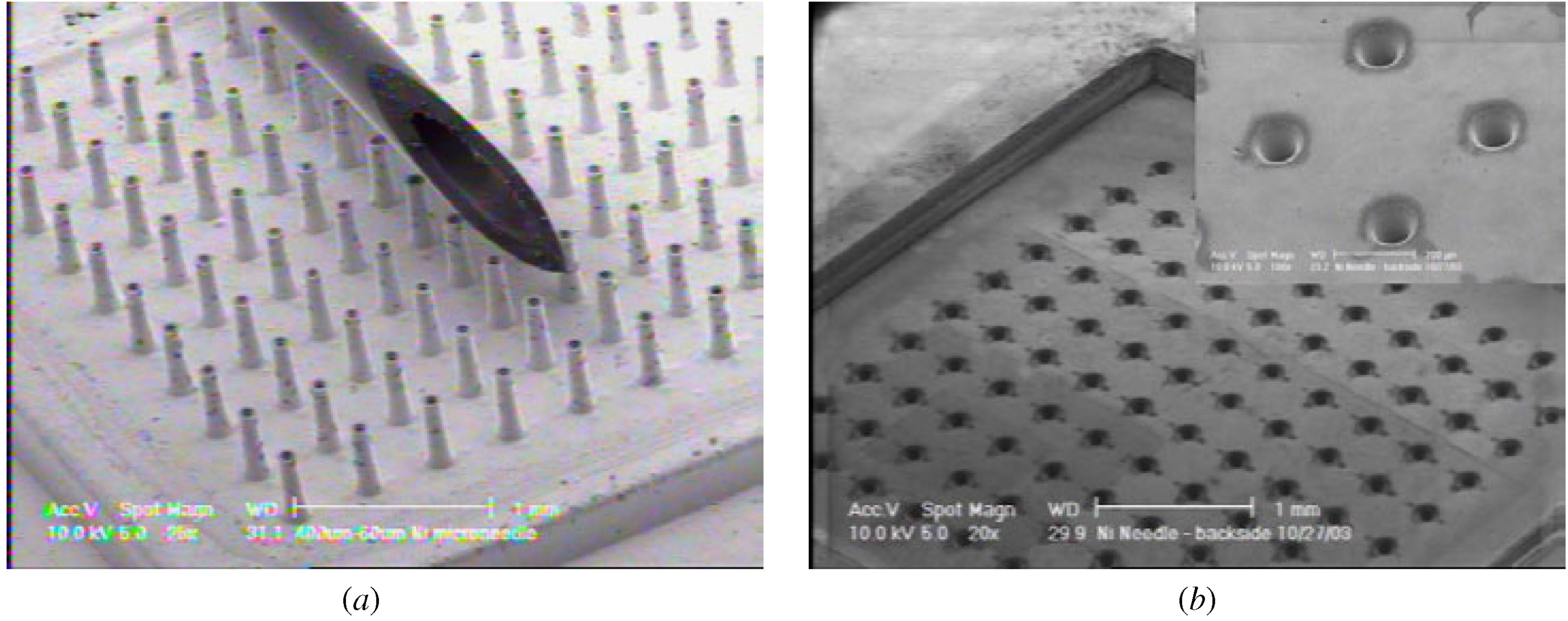
28]. The process was started with a back-side exposure of SU-8 to form a mesa structure. Then, another SU-8 layer was spun coated on top of the first SU-8 mesa and back-side exposed again to create an array of 200–400 μm tall SU-8 tapered pillar structures with taper angles in the range of 3.1°–5°. It was followed by conformal electrodeposition of metal, a mechanical polishing using a planarizing polymeric layer, and all organic layers were removed to create a metallic hollow microneedle array with an integrated fluidic reservoir on the backside. Both 200 and 400 μm tall, 10 by 10 arrays of metallic microneedles with inner diameters of the tip in the range of 33.6–101 μm and wall thickness of 10–20 μm were fabricated (
Figure 6). It was calculated that a single 400 μm tall hollow cylindrical microneedle made of electroplated nickel with a wall thickness of 20 μm, a tapered angle of 3.08° and a tip inner diameter of 33.6 μm has a critical buckling force of 1.8 N.
Figure 5.
Schematic diagrams of the process flow to fabricate a tapered SU-8 pillar structures: (
a) first 200 μm thick SU-8 exposure through a glass substrate; (
b) second 200 μm thick SU-8 layer preparation; (
c) the second SU-8 layer exposure through the glass substrate and the exposed first SU-8 layer to create an array of tapered SU-8 structures; and (
d) a general view of the fabricated double-layered SU-8 on a glass substrate. Reprinted with permission from [
27], copyright 2004 Institute of Physics.
The inclined exposure was not only carried out on the front-side, but on the back-side as well. Sato
et al. [
29,
30] and Yoon
et al. [
31] independently reported, but nearly identical new lithography process in which multiple back-side exposures on SU-8 were carried out with different inclined angle each time to create a complex-shape 3D micromesh structure in microfluidic channel (
Figure 7). The shape and the size of the micromesh were determined by numbers of exposure and irradiation angles of the UV exposure. Sato
et al. further developed the process and demonstrated a completely enclosed monolithic all SU-8 T-shaped microfluidic channel with built-in micromesh in the channel using SU-8 bonding and lift-off resist sacrificial layer [
32]. The organic phase of butyl acetate and the aqueous phase of deionized water with a surfactant were introduced into the microfluidic channel and water droplet fragmentation with the droplet sizes in the range of 30–100 μm were demonstrated. Yoon
et al. further developed the fabrication process to demonstrate many unique microstructures including 600 μm tall various angled out-of-plane SU-8 micro hand and tall high aspect ratio micro column structures (up to 800 μm tall, 40:1 aspect ratio) [
33].
Figure 6.
SEM images of a fabricated microneedle array: (
a) 400 μm tall tapered hollow metallic microneedle array in comparison with a conventional gauge 28 stainless steel needle; (
b) back-side of the microneedle array showing a fluidic reservoir and fluidic channels (through holes). Reprinted with permission from [
27], copyright 2004 Institute of Physics.
Figure 7.
SEM images of (
a) simultaneously fabricated three integrated filters in microfluidic channels with different mesh sizes and (
b) close-up view of the (
left) filter 1, (
middle) filter 2 and (
right) filter 3 which have horizontal diagonal of 57.3 μm, 27.3 μm and 10 μm, respectively. Reprinted with permission from [
33], copyright 2006 IEEE.
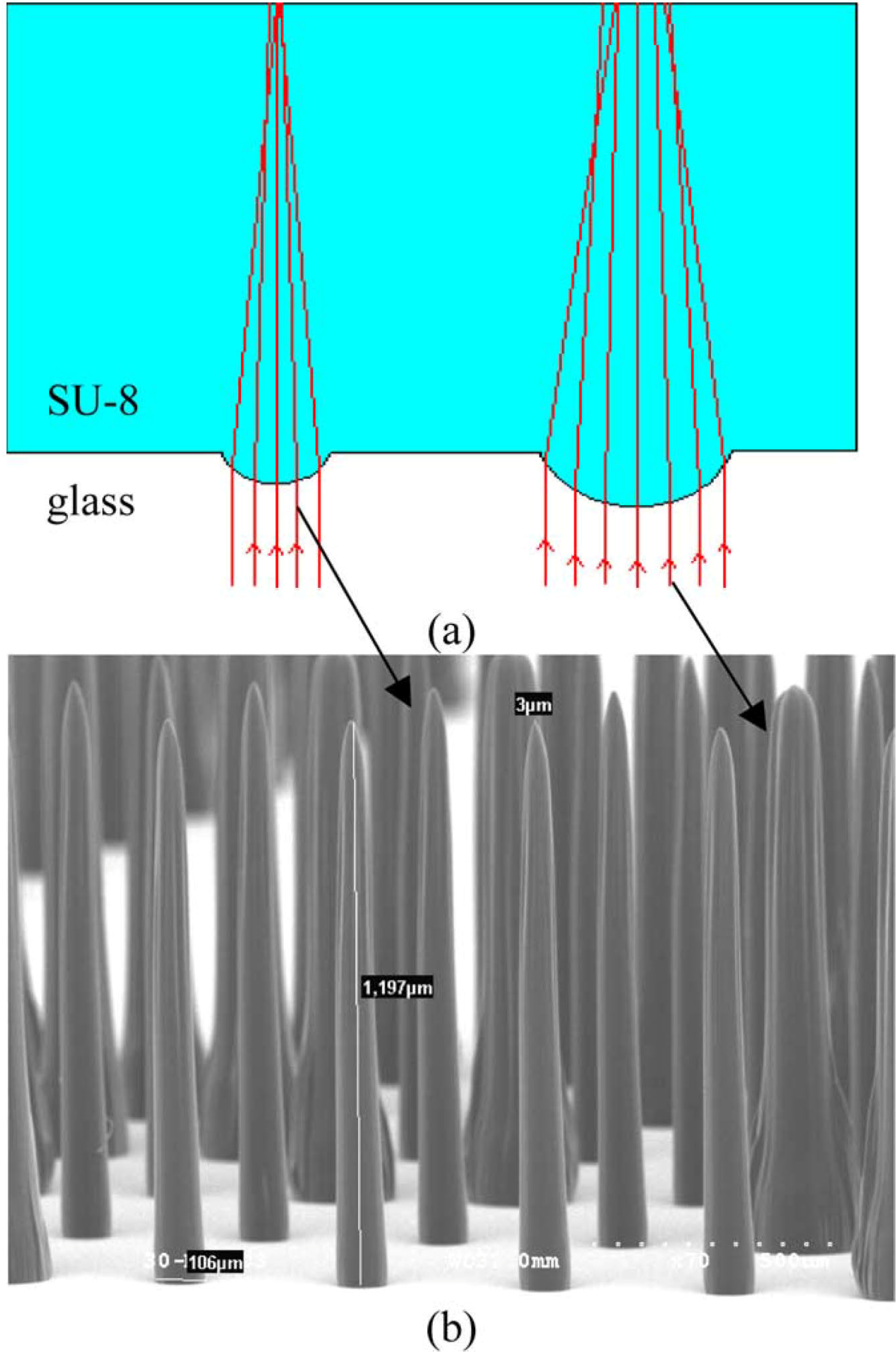
Another interesting SU-8 back-side exposure technique was reported by Park
et al. using an integrated lens on glass substrate [
34]. An array of hemi-spherical micro-lenses (200 μm diameter, 70 μm in depth, 400 μm pitch distance) was fabricated on a glass substrate by isotropic wet etching through a patterned chrome mask layer. SU-8 was then coated on the lens-formed chrome-coated glass substrate and UV exposure was undertaken through the micro-lens array (
Figure 8). This technique yielded a very sharp 1.5 mm tall SU-8 microneedle array. The SU-8 microstructure was also used as a mold and inverse image of the SU-8 mold was replicated in PDMS. Then, the PDMS was used as a template to create biodegradable polymer-based sharp tall microneedle array.
Figure 8.
A conceptual schematic diagram (
a) and an SEM image (
b) of back-side UV exposure with integrated convex lens for creating tall and sharp conical microneedle array with thickness of 1197 μm and tip diameter of 3 μm. Reprinted with permission from [
33], copyright 2006 IEEE.
Figure 8.
A conceptual schematic diagram (
a) and an SEM image (
b) of back-side UV exposure with integrated convex lens for creating tall and sharp conical microneedle array with thickness of 1197 μm and tip diameter of 3 μm. Reprinted with permission from [
33], copyright 2006 IEEE.
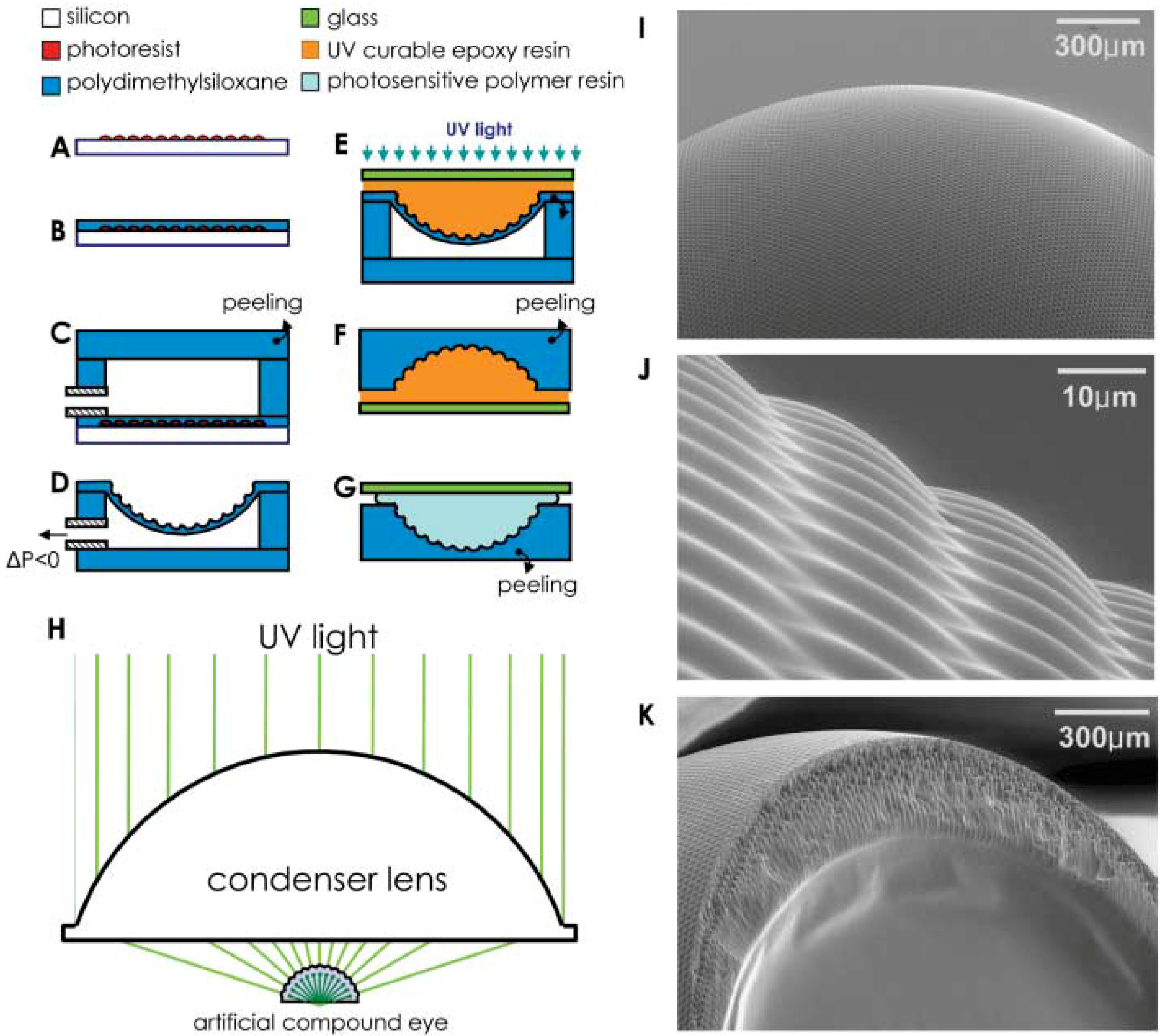
The lens-assisted SU-8 back-side exposure was further utilized with a combination of double cross-linking of SU-8 and multiple unique micro templating process to demonstrate biomimetic artificial compound eyes [
35,
36]. The fabrication was started with formation of an array of micro-lens by photoresist reflow process (
Figure 9A). Then PDMS was used to replicate the inverse image of the micro-lens array and the PDMS replica was placed in a temporary chamber to apply negative pressure to get a deformed hemispherical PDMS mold with the inverse image of the micro-lens array on it (
Figure 9D). Next, SU-8 was used to replicate the inverse image of the PDMS micro-lens template (
Figure 9E) and again the PDMS replication process was repeated to create the final micro-template. SU-8 was then dispensed/soft-baked to have micro-lens (Fresnel number < 10, diameter < 50 μm) array surface SU-8 replica of the PDMS template (
Figure 9G). UV exposure through a high numerical aperture condenser lens was used to have spherical UV irradiation on the micro-lens array surface SU-8 replica (
Figure 9H). The sample was then post-baked (at 90 °C) for photo cross-linking of SU-8 which was followed by hard baking (at 150 °C) for thermal cross-linking of SU-8. The hard baking process seemed to be crucial as this it uses refractive index difference between the photo cross-linked SU-8 region and thermally cross-linked SU-8 region to create waveguide core and waveguide cladding.
Figure 9I–K shows SEM images of the fabricated hemispherical dome-shaped artificial compound eyes with diameter of 2.5 mm.
Figure 9.
Schematic diagrams of the process sequence of the SU-8-based biomimetic artificial compound eyes: (
A) micro-lens array formation by photoresist reflow; (
B) PDMS molding; (
C) PDMS bonding; (
D) PDMS membrane deformation by applied negative pressure; (
E) replication with UV curable polymer resin; (
F) PDMS molding; (
G) SU-8 molding; (
H) UV exposure through a condenser lens; SEM images of an artificial compound eye (
I–
K). Reprinted with permission from [
36], copyight 2006 American Association for the Advancement of Science.
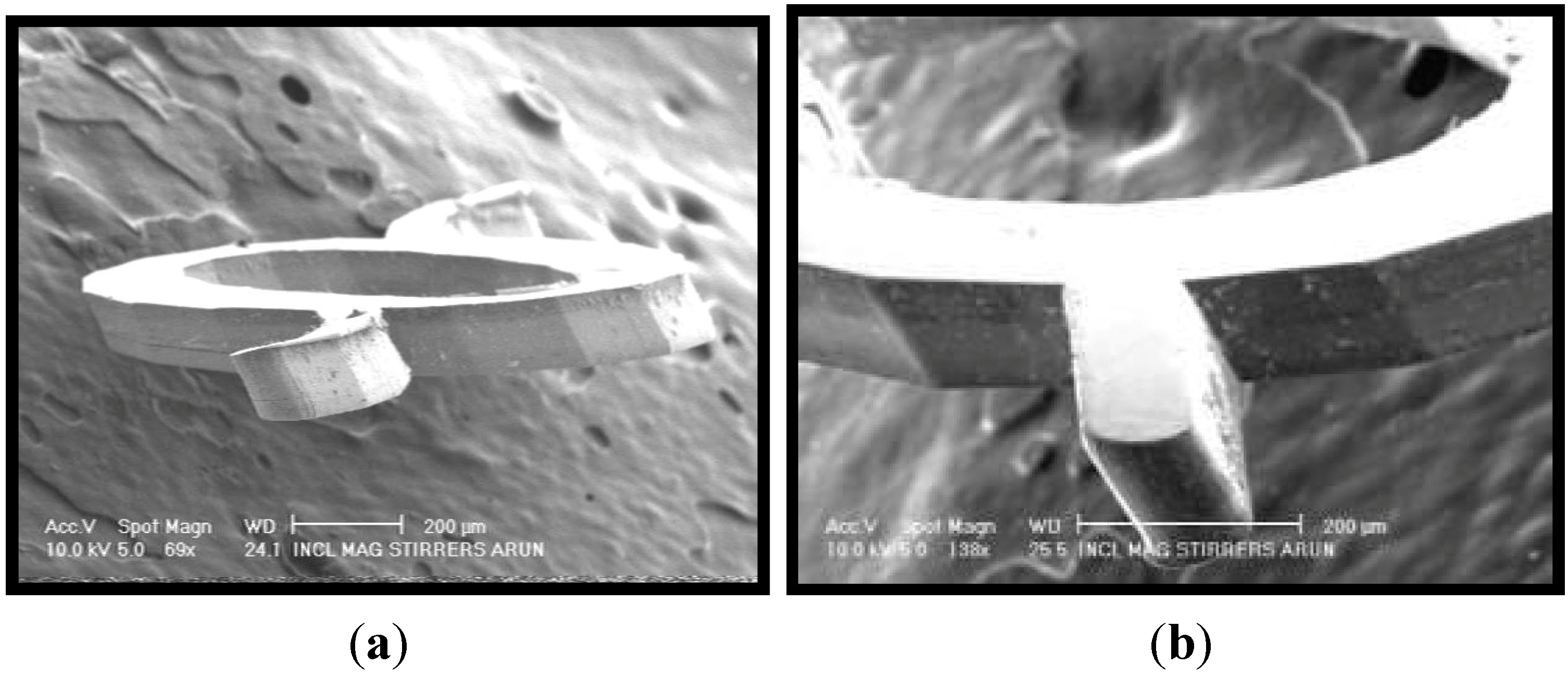
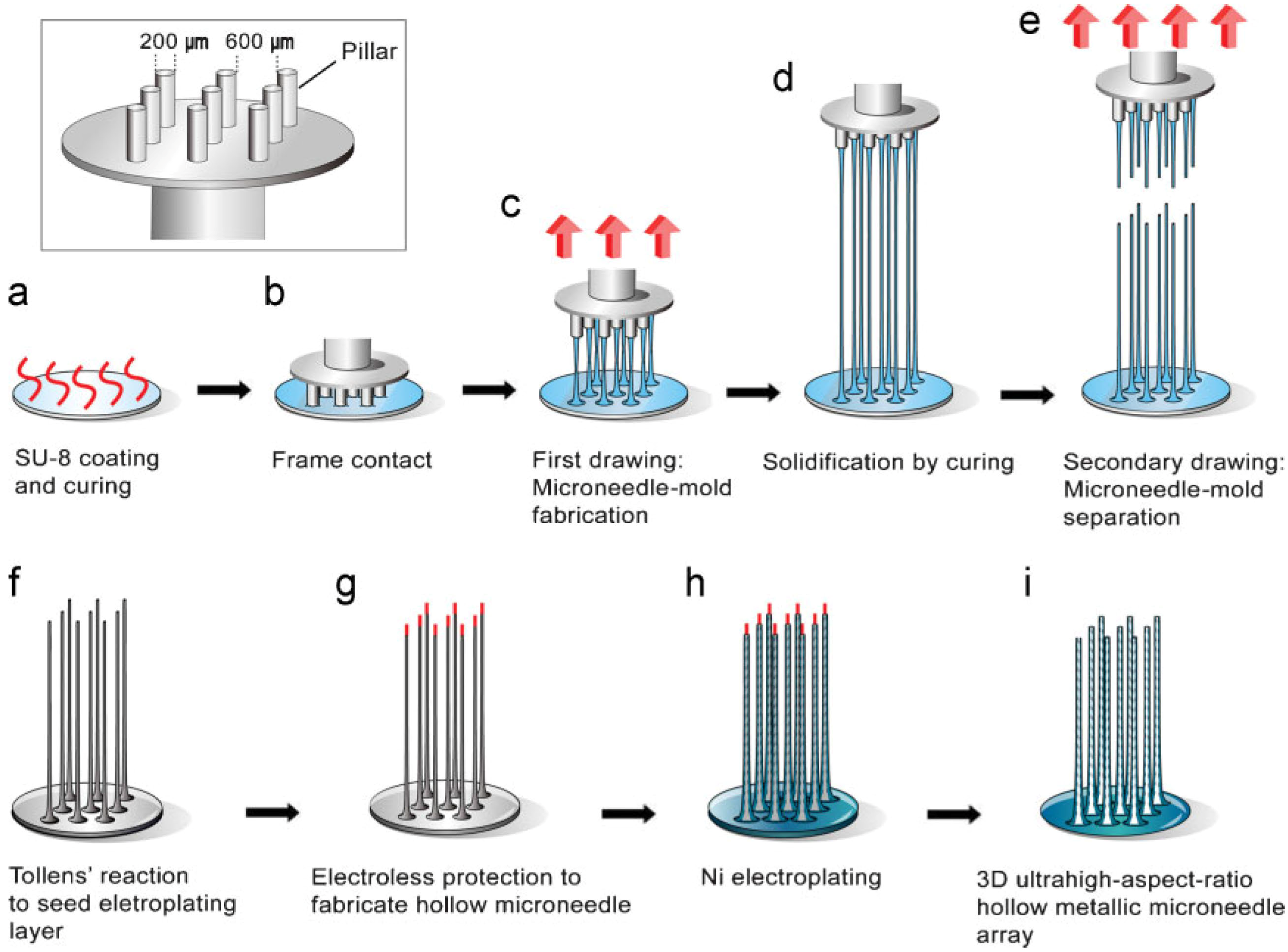
4. Drawing Lithography
Another interesting tweak in SU-8 lithography is “drawing lithography” [
37]. This is not a traditional UV lithography technique, but utilizes mechanical pulling of soft-baked (at 120 °C) SU-8 layer to create extremely tall (~2 mm) high aspect ratio (>100:1) microneedles. It should be noted that this technique can be applied to most thermosetting polymers, but SU-8 was selected due to it is relatively easy to get desirable properties by varying process temperatures. An array of 3 μm × 3200 μm diameter 3 mm tall stainless drills frame was used to make contact on the soft-baked SU-8 and directly pulled in the out-of-plane direction. The pulling rate and temperature were carefully controlled for successful drawing of soft-baked SU-8. Once drawn conical shape SU-8 reached to desired length, drawn SU-8 was thermally cured at room temperature (
Figure 10d). Next, second drawing was carried out with much higher speed than the pulling of soft-baked SU-8 to separate the conical SU-8 microstructure from the stainless drills frame. After the formation of the tall high aspect ratio SU-8 microstructures, seed layer was deposited and tips of the SU-8 microstructures were covered by enamel (
Figure 10g). Then, nickel electroplating was carried out and thermally cured SU-8 and enamel were removed to create ultra-high aspect ratio metallic hollow microneedles (
Figure 10i) which have length of 2 mm, base diameter of 300 μm and flat tip diameter of 20 μm.
Figure 10.
Schematic diagrams of the process sequence of the SU-8 drawing lithography: (
a) SU-8 spin coating; (
b) stainless drill pillar array contact; (
c) drawing of SU-8 layer; (
d) thermal cross-linking of drawn SU-8; (
e) second drawing to create microneedle array; (
f) electroplating seed layer preparation; (
g) protection at the tips of the microneedles; (
h) electroplating; and (
i) hollow microneedle formation by removing SU-8 and tip protection layer. Reprinted with permission from [
37], copyright 2010 WILEY-VCH Verlag GmbH & Co. KGaA, Weinheim.
5. Holographic Interference Lithography
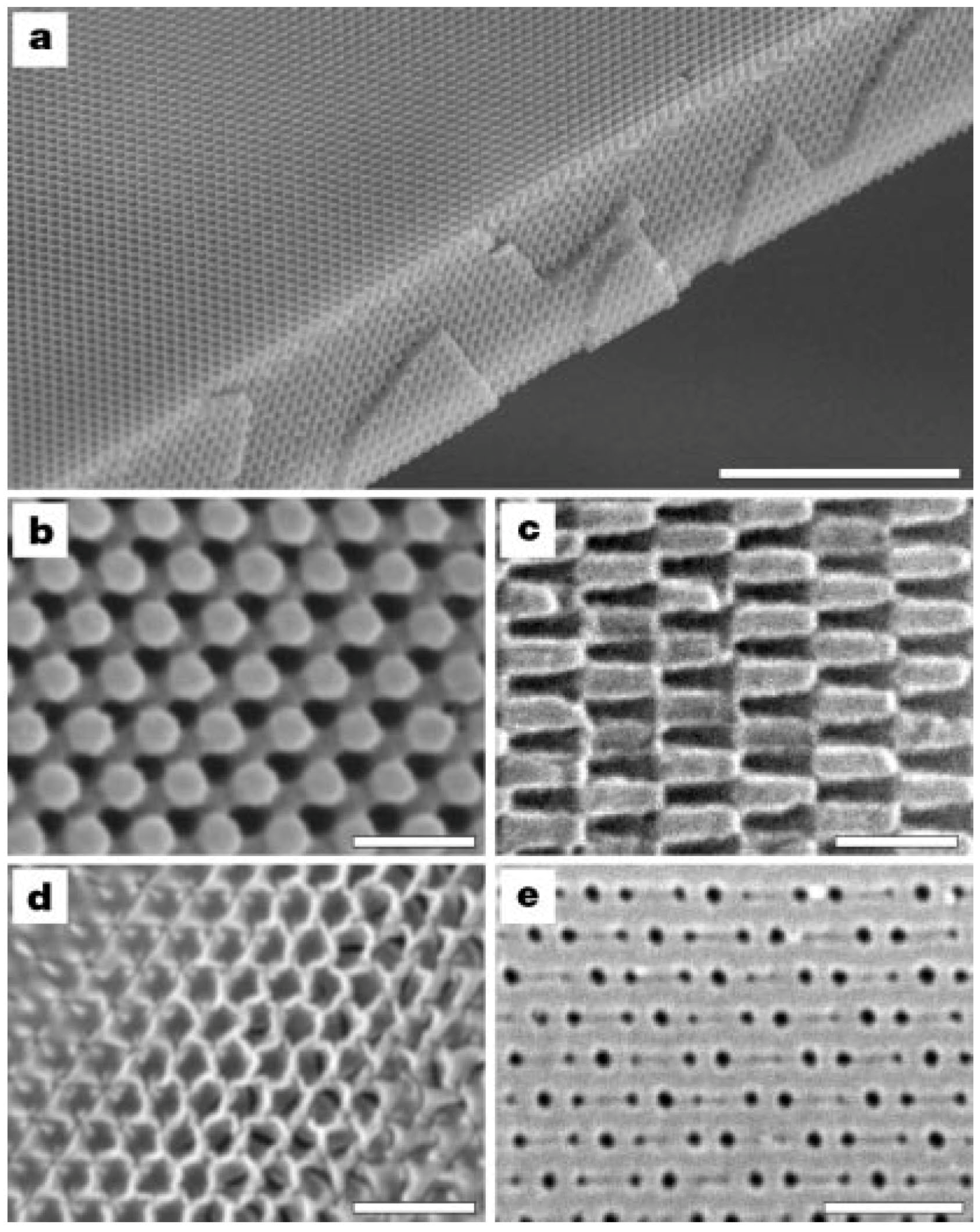
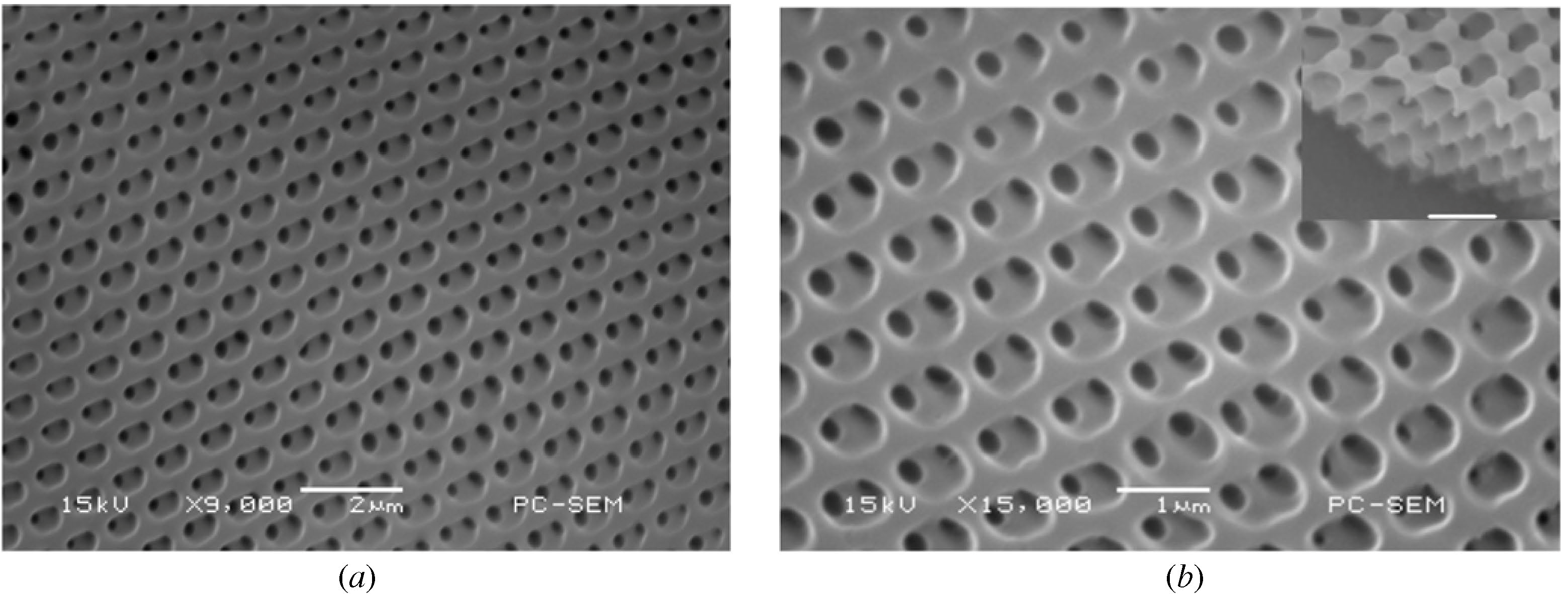
Holographic interference lithography is a mask-less lithography technique that the interference fringes of multiple collimated interfering laser beams are used as exposure energy source of the photoresist. This technique has been widely used for more than four decades to create fine pitch diffraction grating in integrated optics [
38]. Campbell
et al. applied the holographic interference lithography to SU-8 to demonstrate 3D photonic crystal for the visible spectrum [
39]. A neodymium-doped yttrium aluminum garnet (Nd:YAG) laser was frequency-tripled (wavelength of 355 nm) and four laser beams were generated by splitting the UV laser output twice with dielectric beam splitters. The four laser beams were irradiated with specifically designed directions so that the resulting exposed SU-8 patterns have face-centered cubic lattice structure with the lattice constant of 922 nm or a body-centered cubic lattice. The total UV exposure dose in SU-8 at the four beam interfered region was in the range 80–200 mJ/cm
2 to achieve the required polymer/air photonic crystal structure. The highly exposed region of SU-8 was remained after developing process which resulted in 3D periodic cross-linked SU-8 with air-filled voids (
Figure 11). Since the UV exposed SU-8 has refractive index at around 1.6, this 3D structure makes periodic refractive index contrast of SU-8/air (index of 1.0). The SU-8/air 3D photonic crystal was tested with a helium-neon laser (wavelength of 633 nm) to show its Bragg scattering characteristics.
Figure 11.
SEM images of SU-8/air 3D photonic crystals generated by holographic lithography. (
a) Photonic crystal generated in 10 μm thick SU-8 (scale bar: 10 μm); (
b) close-up of a (111) surface (scale bar: 1 μm); (
c) close-up of a (
) surface (scale bar: 1 μm); (
d) inverse replica in titania made by using the polymeric structure as a template; (
e) (
) surface of a body-centered cubic SU-8/air photonic crystal (scale bar: 1 μm). Reprinted with permission from [
39], copyright 2000 Macmillan Publishers Ltd.
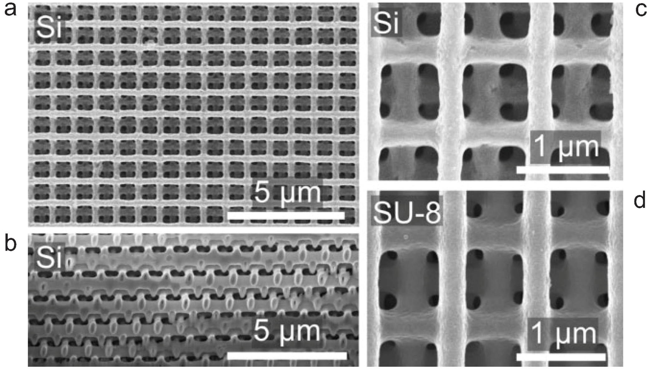
The SU-8/air periodic structure formed by the holographic interference lithography was well demonstrated as a photonic crystal, but the refractive index contrast between SU-8 and air is not as great as other photonic crystals like silicon/air photonic crystal. There have been efforts to use 3D SU-8 photonic crystal as a template and infiltrate other high refractive index material to realize high index contrast photonic crystals. Tétreault
et al. fabricated SU-8 3D photonic crystal using two-photon interference lithography by 120 fs pulses at 800 nm wavelength Ti:sapphire laser. The sample was then infiltrated by SiO
2 using chemical vapor deposition (CVD) and the 3D SU-8 photonic crystal template was removed by dry etching. Then, again the SiO
2 structure was used as a template and hydrogenated amorphous silicon (a-Si:H) was infiltrated into the SiO
2 template using low-pressure CVD. Finally, the SiO
2 template was etched away using hydrofluoric acid (HF) which yielded an a-Si:H/air 3D photonic crystal [
40].
Figure 12c,d shows a side-by-side comparison between the final a-Si:H woodpile phonic crystal and the original SU-8 woodpile photonic crystal which shows precise patterning in 3D deep sub-micron structures.
Holographic interference lithography patterning fidelity has been improved over the years with various techniques. One of the techniques employed was to utilize lens array [
41]. Four beams and four lenses were used to achieve a so-called umbrella-type intensity distribution to create a SU-8/air 3D face-centered cubic (FCC) photonic crystal structure (
Figure 13).
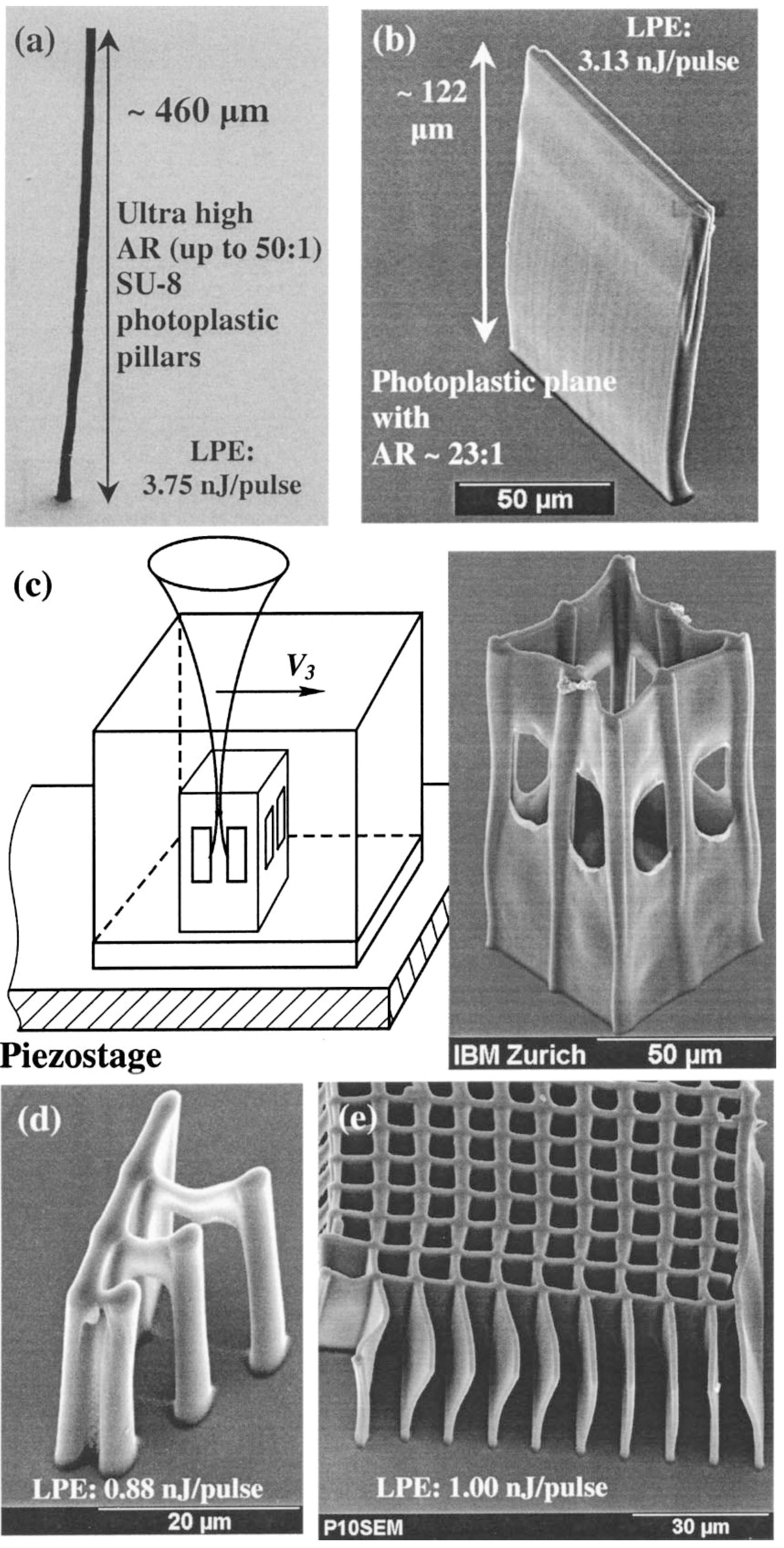
SU-8 laser holographic interference lithography was also utilized to create high aspect ratio 3D microstructures with sub-diffraction-limit resolution. Teh
et al. used ~800 nm Ti:sapphire laser and two photon absorption method to demonstrate tall (up to 460 μm thick) high aspect ratio (up to 50:1) SU-8 microstructures (
Figure 14).
Although it is not holographic interference lithography, one of the interesting mask-less direct lithography is UV exposure using light emitting diode (LED). This technique is interesting as it does not require a typical stand-alone mask-aligner. Jeon
et al. directly integrated UV-curable polymer microlens array onto a matrix-addressable 368-nm-wavelength, LED device containing 64 × 64 micropixel elements to create an array of collimated UV illumination. This microlens integrated LED array was utilized as a direct photolithography tool using a positive photoresist and demonstrated simple circular pattern with diameter of 16 μm [
42]. Guijt
et al. used a commercially available $20 UV LED and collimated light illumination from the LED using a pinhole and a plastic tube and a microscope objective. The collimated UV light was exposed on a layer of SU-8 with a motorized stage to demonstrate 35 μm SU-8 pattern which was used as a template to fabricate a simple PDMS microfluidic channel [
43].
Figure 12.
SEM images of a-Si:H woodpile photonic crystal using SU-8 template: (
a) top view of the a-Si:H woodpile photonic crystal; (
b) cross-sectional view of the a-Si:H photonic crystal; (
c,
d) close-up views of the replicated a-Si:H and original SU-8 woodpile structures. Reprinted with permission from [
40], copyright 2006 WILEY-VCH Verlag GmbH & Co. KGaA, Weinheim.
Figure 13.
SEM images of 3D FCC photonic crystal fabricated in SU-8. Reprinted with permission from [
41], copyright 2012 Institute of Physics.
Figure 13.
SEM images of 3D FCC photonic crystal fabricated in SU-8. Reprinted with permission from [
41], copyright 2012 Institute of Physics.
Figure 14.
3D high aspect ratio SU-8 microstructures using two photon absorption lithography technique. (
a) SEM image of a 50:1 aspect ratio SU-8 pillar measuring; (
b) SEM image of a SU-8 vertical plane (122 μm high, aspect ratio of 23:1); (
c) a 132 × 50 × 50 μm
3 cage structure; (
d) suspended SU-8 bridges of various lengths from 5 to 15 μm long; and (
e) a preliminary SU-8 photonic crystal structure with a periodicity of 10 μm. Reprinted with permission from [
44], copyright 2004, AIP Publishing LLC.
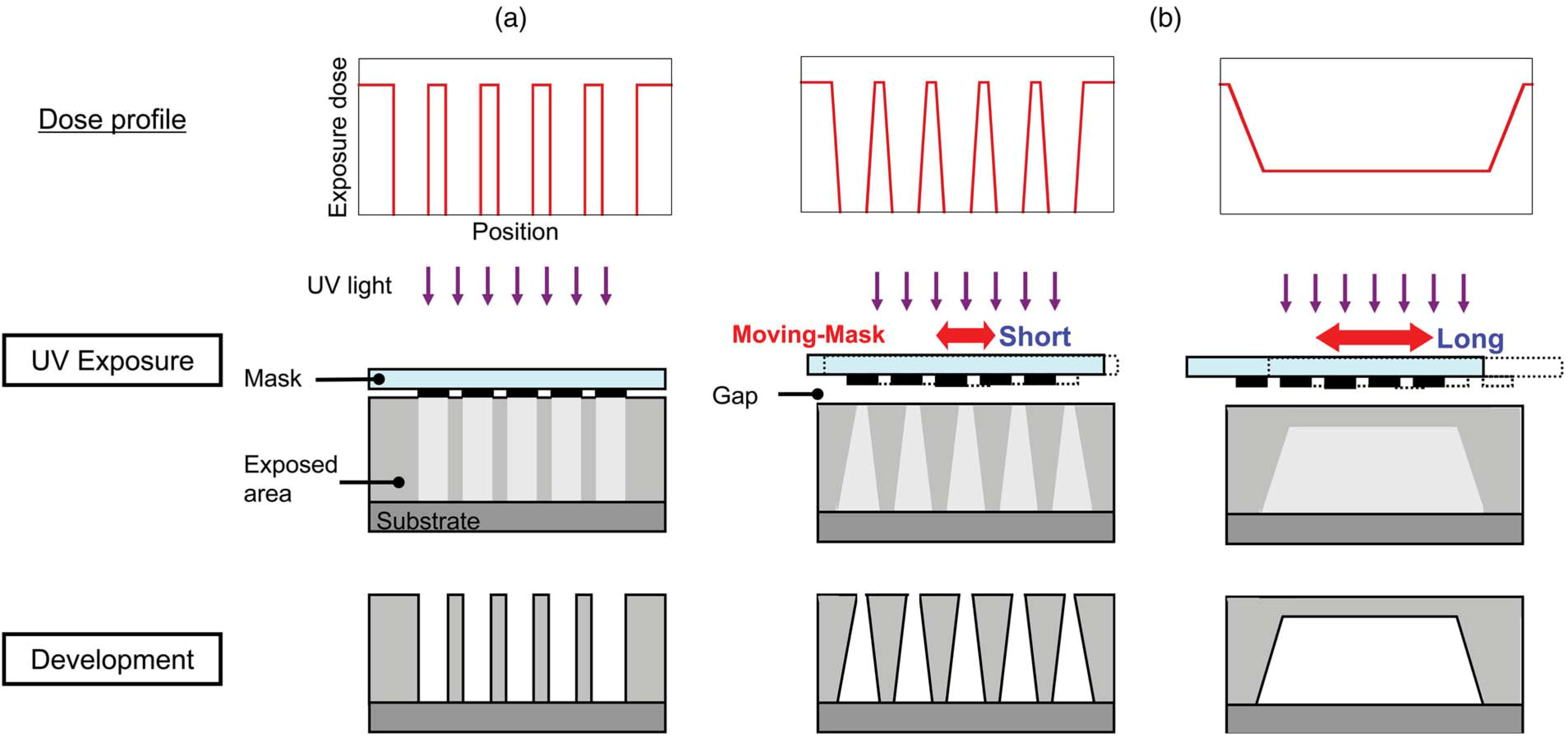
6. Moving-Mask Lithography and Maskless Grayscale Lithography
Another unique lithography technique is UV dosage control by a moving-mask lithography (
Figure 15) [
45]. The moving-mask lithography was first demonstrated in deep X-ray lithography to realize 3D tall inclined polymethyl methacrylate (PMMA) microstructures [
46]. Various conical shape and truncated conical shape PMMA microstructures with height of 100–300 μm and a diameter of the top and the bottom of truncated conical structures between 0 and 310 μm were fabricated. The moving-mask technique was then applied to UV lithography to demonstrate unique 3D inclined 50 μm thick positive-tone photoresist microstructures [
47]. This technique was again applied to precisely control UV dosage along specific areas of negative-tone photoresist TMMR (Tokyo Ohka Kogyo Company, Ltd., Tokyo, Japan), which is quite similar to SU-8, to demonstrate embedded microfluidic channel in a single moving-mask exposure on a single-layer of photoresist [
45]. For example, the moving-mask lithography was utilized to realize lightly exposed semi-cross-linked region in the middle (
Figure 15b) and high exposure dose at the side. In this way, the middle region forms a top-membrane which is permeable to the developer. Developer can permeate through the top-membrane and the permeated developer dissolves the uncross-linked photoresist which yields a completely enclosed microfluidic channel in a single layer in a single exposure process.
UV dosage control is also possible in grayscale lithography [
48]. Rammohan
et al. utilized the use of grayscale maskless lithography in a single-layer of SU-8 to demonstrate 3D microstructures such as air-suspended cantilevers, microneedles and embedded microfluidic channels [
49]. In the case of microfluidic channels, micro ridges and micro pillars with different exposure doses than the sidewall were utilized to form passive mixing microfluidic channels.
Figure 15.
Exposure dose profile on the photoresist and conceptual illustration of 3D thick microstructures using a negative-tone photoresist: (
a) standard photolithography and (
b) moving-mask lithography. Reprinted with permission from [
45], copyright 2010 IEEE.
Figure 15.
Exposure dose profile on the photoresist and conceptual illustration of 3D thick microstructures using a negative-tone photoresist: (
a) standard photolithography and (
b) moving-mask lithography. Reprinted with permission from [
45], copyright 2010 IEEE.
7. Conclusions
For the past 15 years, several unconventional lithography techniques have been developed for SU-8 to realize unique 3D microstructures. With these new lithography techniques, many innovative 3D microstructures have been demonstrated including sharp out-of-plane microneedle arrays, microfluidic filters, cell sorters, micro-mixers, artificial compound eyes, and 3D photonic crystals for visible wavelengths. It seems like these new lithography techniques for SU-8 is mature and the micro-fabrication community is in the next phase of applying these already developed lithography techniques to realize truly unique structures essential for certain applications. It is our view that applications demonstrated so far using these unconventional tweaks applied for SU-8 lithography are humble starting point and these techniques will have far-reaching impact not just for MEMS community but for entire micro- and nano-fabrication community.


