

Design and Modeling of Piezoelectric Nanofilm Actuators for Low-Voltage Powered Microrobots
Abstract
1. Introduction
2. Theoretical Model for Multilayer Piezoelectric Microactuators
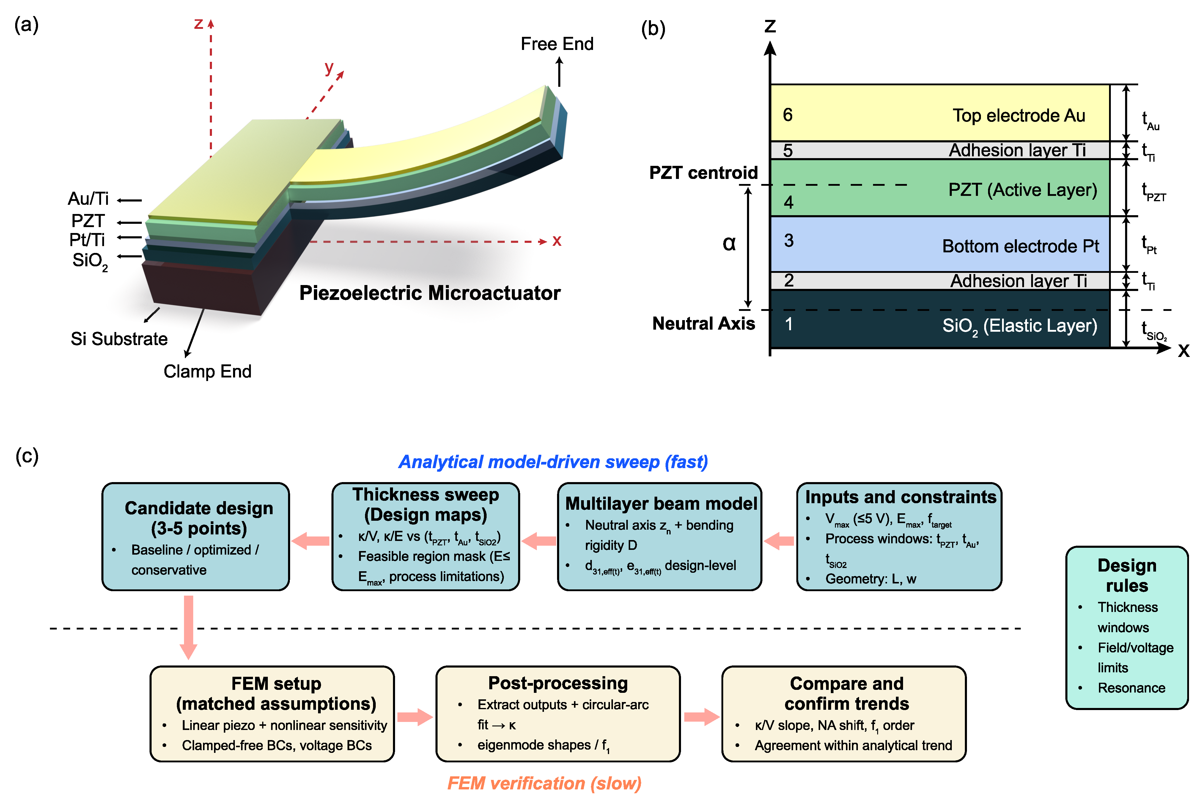
2.1. The Multimorph Structure of Piezoelectric Microactuators
2.2. Analysis of Bending Curvature Based on a Multilayer Euler–Bernoulli Beam Model
2.2.1. Curvature Expression and Term Definitions
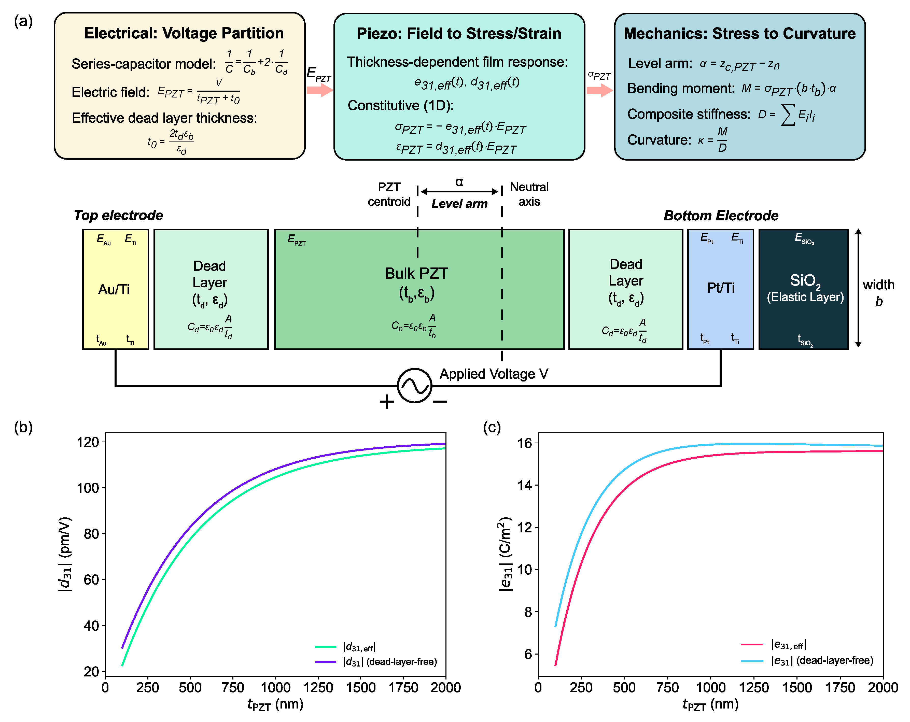
2.2.2. Thickness-Dependent Piezoelectric Coefficients
2.2.3. Evaluation of Neutral-Axis Coordinate and Composite Bending Rigidity
2.3. Electromechanical Simulation Using the Finite Element Method
2.4. Design Constraints and Curvature Metrics
3. Results
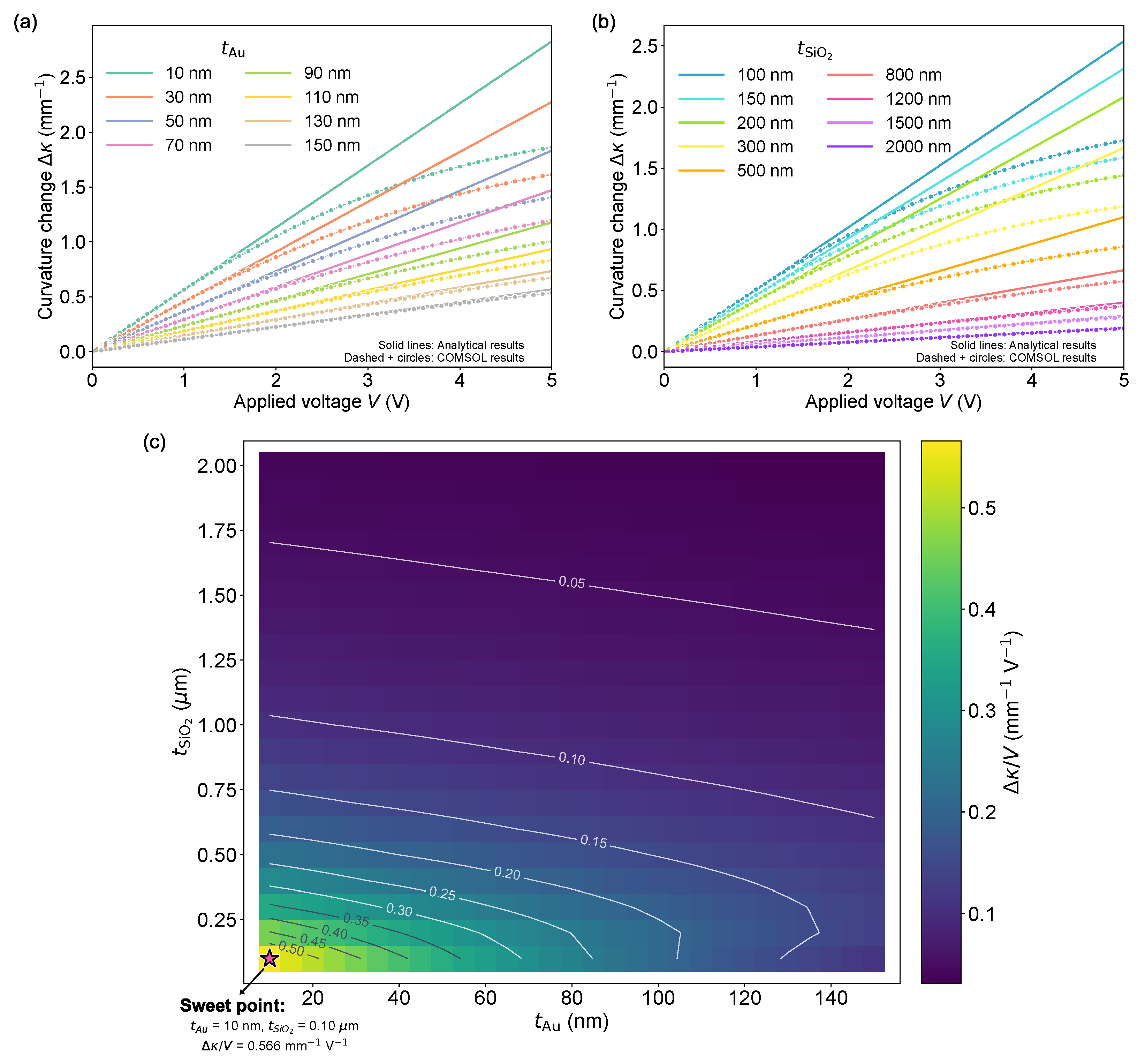
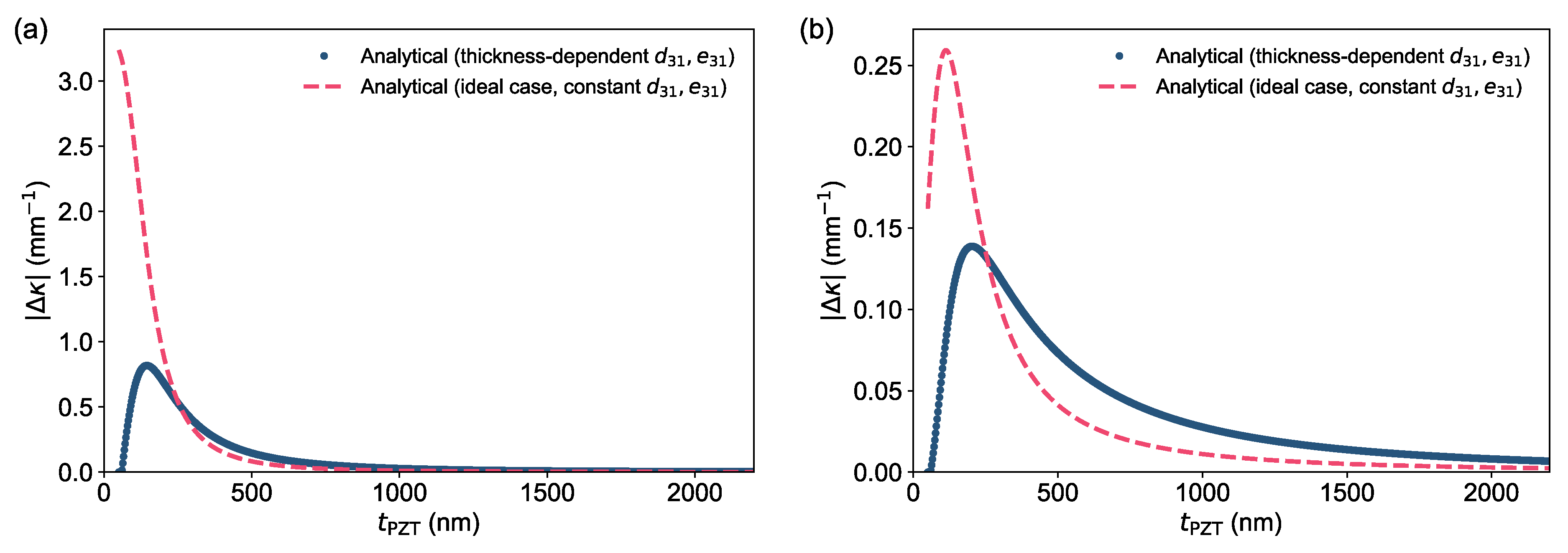
3.1. Curvature–Thickness Relationship Based on the Multilayer Beam Model
3.2. Influence of Passive-Layer Thicknesses Revealed by FEM-Based Neutral-Axis Engineering
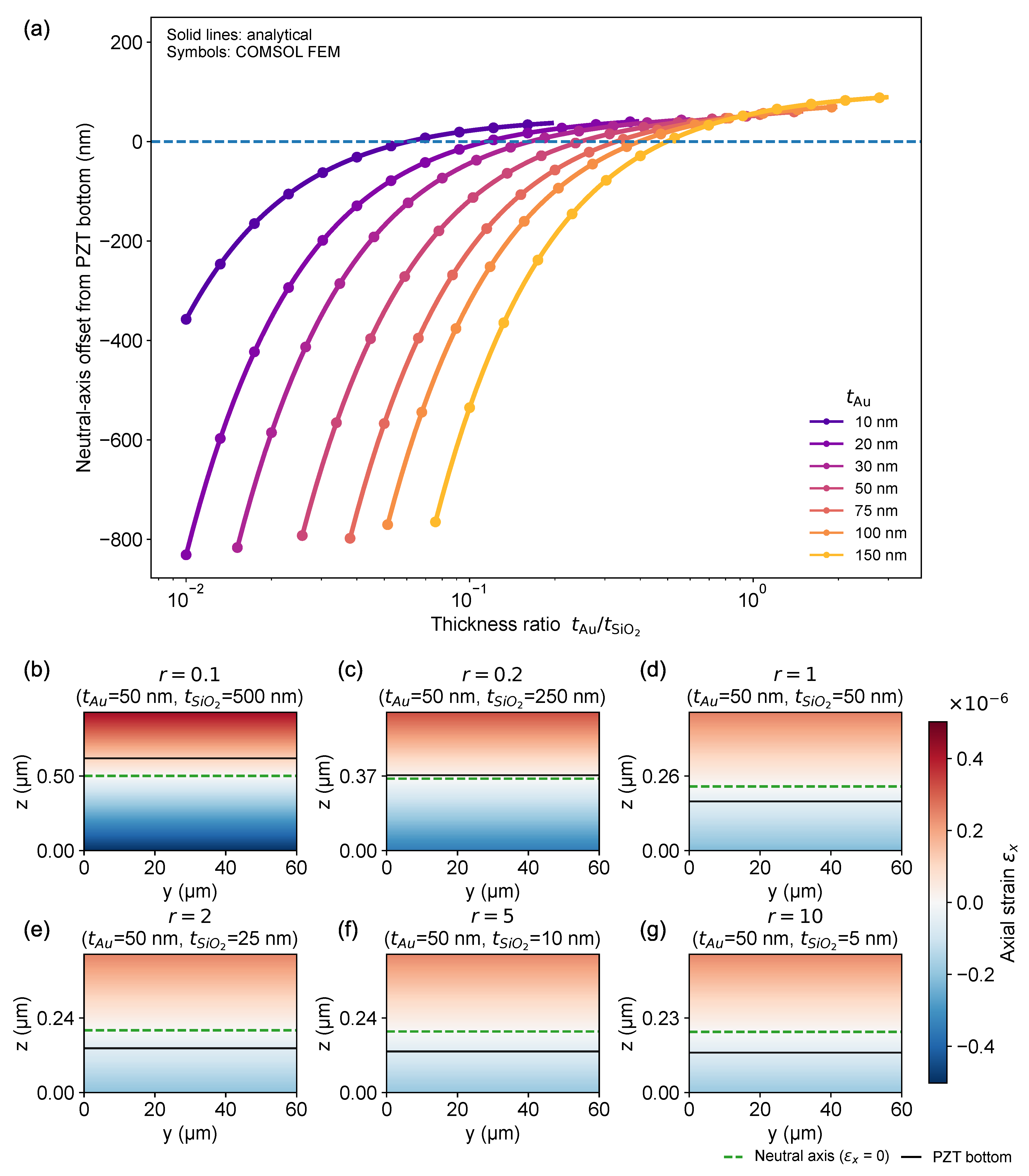
3.3. Neutral-Axis Migration and Strain-Field Interpretation
3.4. Electromechanical Response
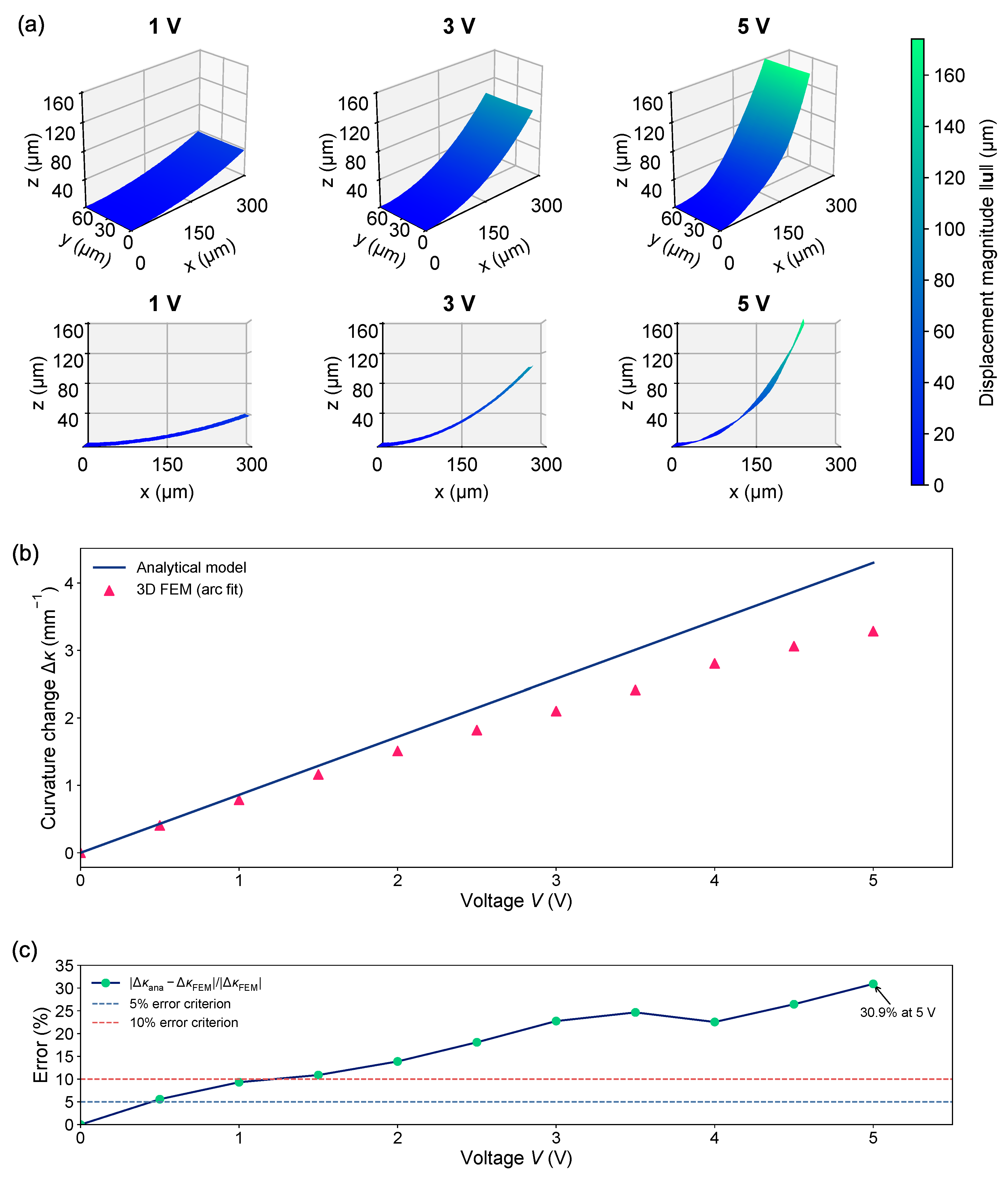
3.4.1. Curvature Definition and Extraction
3.4.2. Analytical vs. FEM Predictions
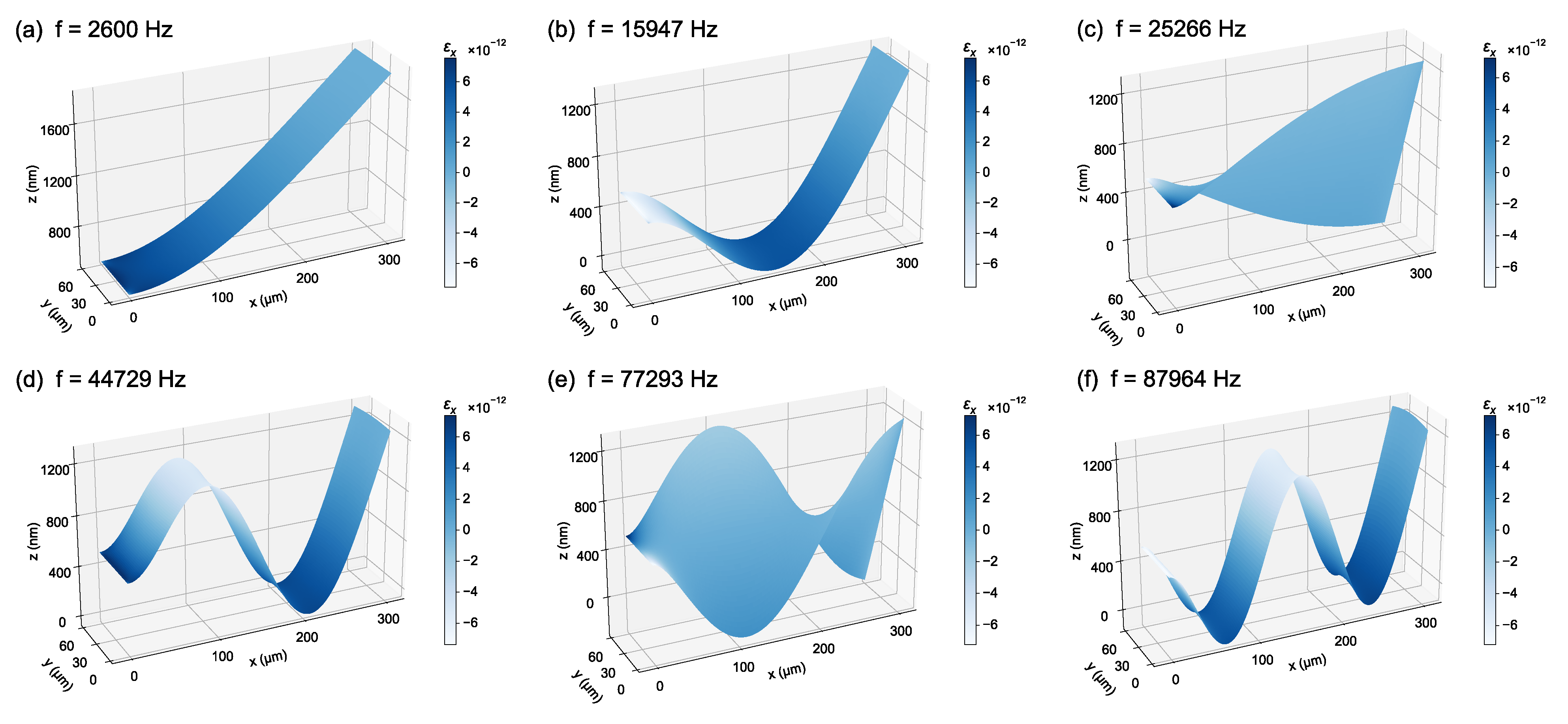
3.5. Eigenfrequency Analysis and Modal Shape Characterization
4. Discussion
4.1. Relation to Previous Multilayer Models and Actuator Designs
4.2. Design Implications for Low-Voltage, High-Curvature Piezoelectric Microactuators
4.3. Model Limitations and Outlook
5. Conclusions
- (1)
- PZT thickness exhibits a non-monotonic optimum once nanofilm coupling degradation is included. Therefore, the thinnest feasible film is not necessarily the best choice for curvature per volt.
- (2)
- Top-electrode thinning is a high-leverage design knob because it simultaneously reduces parasitic stiffness and shifts the neutral axis in a way that increases the effective bending moment arm of the PZT layer.
- (3)
- Dielectric/support thickness must be tightly controlled since excessive passive-layer thickness rapidly stiffens the stack and suppresses curvature despite low-voltage drive.
Author Contributions
Funding
Institutional Review Board Statement
Informed Consent Statement
Data Availability Statement
Acknowledgments
Conflicts of Interest
Abbreviations
| PZT | Lead zirconate titanate (Pb(Zr,Ti)O3) |
| FEM | Finite element method |
| MEMS | Micro-electro-mechanical system |
| COMSOL | COMSOL Multiphysics |
| 1D | One-dimensional |
| 2D | Two-dimensional |
| 3D | Three-dimensional |
References
- Trolier-McKinstry, S.; Muralt, P. Thin Film Piezoelectrics for MEMS. J. Electroceramics 2004, 12, 7–17. [Google Scholar] [CrossRef] [Scilit]
- Liu, J.; Tan, H.; Zhou, X.; Ma, W.; Wang, C.; Tran, N.-M.-A.; Lu, W.; Chen, F.; Wang, J.; Zhang, H. Piezoelectric Thin Films and Their Applications in MEMS: A Review. J. Appl. Phys. 2025, 137, 020702. [Google Scholar] [CrossRef] [Scilit]
- Pulskamp, J.S.; Polcawich, R.G.; Dubey, M. Piezoelectric PZT MEMS technologies for small-scale robotics and RF applications. MRS Bull. 2012, 37, 1062–1070. [Google Scholar] [CrossRef] [Scilit]
- Zhou, M.; Fan, Z.; Ma, Z.; Zhao, H.; Guo, Y.; Hong, K.; Li, Y.; Liu, H.; Wu, D. Design and Experimental Research of a Novel Stick-Slip Type Piezoelectric Actuator. Micromachines 2017, 8, 150. [Google Scholar] [CrossRef] [Scilit]
- Zhao, Y.; Huang, X.; Li, Y.; Wang, G.; Hao, K. Design and Control of a Piezoelectric-Driven Microgripper Perceiving Displacement and Gripping Force. Micromachines 2020, 11, 121. [Google Scholar] [CrossRef] [Scilit]
- Lu, X.; Wu, Y.; Chen, J.; Chen, Y.; Wu, X.; Xiao, D. Insect-scale flapping-wing MAVs with variable transmission ratio and wingspan: Achieving payload adaptability, and self-stabilizing hovering. Microsystems Nanoeng. 2026, 12, 22. [Google Scholar] [CrossRef] [Scilit]
- Nishimura, N.; Hida, D.; Kanno, I. Fabrication of PZT thin film actuator for Insect scale robot. Proc. JSME Mech. Eng. Congr. Jpn. 2017, 2017, G1600102. [Google Scholar] [CrossRef] [Scilit]
- Steltz, E.; Wood, R.J.; Fearing, R.S. Optimal Energy Density Piezoelectric Bending Actuators. Sens. Actuators A Phys. 2005, 119, 476–488. [Google Scholar] [CrossRef] [Scilit]
- Wood, R.J.; Steltz, E.; Fearing, R.S. Nonlinear Performance Limits for High Energy Density Piezoelectric Bending Actuators. In Proceedings of the 2005 IEEE International Conference on Robotics and Automation (ICRA), Barcelona, Spain, 18–22 April 2005. [Google Scholar] [CrossRef] [Scilit]
- Karpelson, M.; Wei, G.-Y.; Wood, R.J. Driving High Voltage Piezoelectric Actuators in Microrobotic Applications. Sens. Actuators A: Phys. 2012, 176, 78–89. [Google Scholar] [CrossRef] [Scilit]
- Steltz, E.; Seeman, M.; Avadhanula, S.; Fearing, R.S. Power Electronics Design Choice for Piezoelectric Microrobots. In Proceedings of the IEEE/RSJ International Conference on Intelligent Robots and Systems (IROS), Beijing, China, 9–15 October 2006; pp. 1322–1328. [Google Scholar] [CrossRef] [Scilit]
- Kurchania, R.; Milne, S.J. Characterization of Sol-Gel Pb(Zr0.53Ti0.47)O3 Films in the Thickness Range 0.25–10 μm. J. Mater. Res. 1999, 14, 1852–1859. [Google Scholar] [CrossRef] [Scilit]
- Duval, F.F.C.; Wilson, S.A.; Ensell, G.; Evanno, N.M.P.; Cain, M.G.; Whatmore, R.W. Characterisation of PZT thin film micro-actuators using a silicon micro-force sensor. Sens. Actuators A Phys. 2007, 133, 35–44. [Google Scholar] [CrossRef] [Scilit]
- Moriyama, M.; Kawai, Y.; Tanaka, S.; Esashi, M. Low-voltage-driven thin film PZT stacked actuator for RF-MEMS switches. IEEJ Trans. Sens. Micromachines 2012, 132, 282–287. [Google Scholar] [CrossRef] [Scilit]
- Kim, D.-J.; Park, J.-H.; Shen, D.-Y.; Yoon, S.-G.; Lee, J.-H. Thickness Dependence of Submicron Thick Pb(Zr0.3Ti0.7)O3 Films on Piezoelectric Properties. Ceram. Int. 2008, 34, 1909–1915. [Google Scholar] [CrossRef] [Scilit]
- Nguyen, M.D.; Dekkers, M.; Vu, H.N.; Rijnders, G. Film-Thickness and Composition Dependence of Epitaxial Thin-Film PZT-Based Mass-Sensors. Sens. Actuators A Phys. 2013, 199, 98–105. [Google Scholar] [CrossRef] [Scilit]
- DeVoe, D.L.; Pisano, A.P. Modeling and Optimal Design of Piezoelectric Cantilever Microactuators. J. Microelectromech. Syst. 1997, 6, 266–270. [Google Scholar] [CrossRef] [Scilit]
- Smits, J.G.; Choi, W. The Constituent Equations of Piezoelectric Heterogeneous Bimorphs. IEEE Trans. Ultrason. Ferroelectr. Freq. Control 1991, 38, 256–270. [Google Scholar] [CrossRef] [Scilit]
- Smits, J.G. The Constituent Equations of Piezoelectric Bimorphs. Sens. Actuators A Phys. 1991, 28, 41–61. [Google Scholar] [CrossRef] [Scilit]
- Kamlah, M. Ferroelectric and Ferroelastic Piezoceramics—Modeling of Electromechanical Hysteresis Phenomena. Contin. Mech. Thermodyn. 2001, 13, 219–268. [Google Scholar] [CrossRef] [Scilit]
- Ledermann, N.; Muralt, P.; Baborowski, J.; Gentil, S.; Mukati, K.; Cantoni, M.; Seifert, A.; Setter, N. (100)-Textured, Piezoelectric Pb(Zrx,Ti1-x)O3 Thin Films for MEMS: Integration, Deposition and Properties. Sens. Actuators A Phys. 2003, 105, 162–170. [Google Scholar] [CrossRef] [Scilit]
- Tyholdt, F.; Calame, F.; Prume, K.; Ræder, H.; Muralt, P. Chemically Derived Seeding Layer for (100)-Textured PZT Thin Films. J. Electroceram. 2007, 19, 311–314. [Google Scholar] [CrossRef] [Scilit]
- Ababneh, A.; Al-Omari, A.N.; Dagamseh, A.M.K.; Tantawi, M.; Pauly, C.; Mücklich, F.; Feili, D.; Seidel, H. Electrical and Morphological Characterization of Platinum Thin-Films with Various Adhesion Layers for High Temperature Applications. Microsyst. Technol. 2017, 23, 703–709. [Google Scholar] [CrossRef] [Scilit]
- Schaefer, B.T.; Cheung, J.; Ihlefeld, J.F.; Jones, J.L.; Nagarajan, V. Stability and Dewetting Kinetics of Thin Gold Films on Ti, TiOx and ZnO Adhesion Layers. Acta Mater. 2013, 61, 7841–7848. [Google Scholar] [CrossRef] [Scilit]
- Thompson, C.V. Solid-State Dewetting of Thin Films. Annu. Rev. Mater. Res. 2012, 42, 399–434. [Google Scholar] [CrossRef] [Scilit]
- Haynes, W.M. CRC Handbook of Chemistry and Physics, 97th ed.; CRC Press: Boca Raton, FL, USA, 2016. [Google Scholar]
- Hopcroft, M.A.; Nix, W.D.; Kenny, T.W. What Is the Young’s Modulus of Silicon? J. Microelectromechanical Syst. 2010, 19, 229–238. [Google Scholar] [CrossRef] [Scilit]
- Wilke, R.H.T.; Moses, P.J.; Jousse, P.; Yeager, C.; Trolier-McKinstry, S. Wafer Mapping of the Transverse Piezoelectric Coefficient, e31,f, Using the Wafer Flexure Technique with Sputter Deposited Pt Strain Gauges. Sens. Actuators A Phys. 2012, 173, 152–157. [Google Scholar] [CrossRef] [Scilit]
- Yang, C.; Zhao, L.; He, J.; Gan, J.; Bao, A.; You, Z.; Gao, Y.; Kanno, I.; Lu, Y. A wafer-level characterization method of thin film transverse piezoelectric coefficient evaluation. Sens. Actuators A Phys. 2024, 378, 115821. [Google Scholar] [CrossRef] [Scilit]
- Lei, S.; Valenzuela Garzon, A.; Zachary, S.; Yu, J.; Oldham, K.R. Polymer-Reinforced Micromachined Thin-Film PZT Unimorph Arrays for Millimeter-Scale Actuation. In Proceedings of the IEEE International Conference on Manipulation, Automation and Robotics at Small Scales (MARSS), West Lafayette, IN, USA, 28 July–1 August 2025. [Google Scholar] [CrossRef] [Scilit]
- Yamashita, K.; Okuyama, M. Characterization of Piezoelectric Property of Sol-Gel PZT Thin Films and Its Improvement by Poling. IEEJ Trans. SM 2004, 124, 124–128. [Google Scholar] [CrossRef] [Scilit]
- Kim, D.M.; Eom, C.B.; Nagarajan, V.; Ouyang, J.; Ramesh, R.; Vaithyanathan, V.; Schlom, D.G. Thickness Dependence of Structural and Piezoelectric Properties of Epitaxial Pb(Zr0.52Ti0.48)O3 Films on Si and SrTiO3 Substrates. Appl. Phys. Lett. 2006, 88, 142904. [Google Scholar] [CrossRef] [Scilit]
- Dawber, M.; Rabe, K.M.; Scott, J.F. Physics of Thin-Film Ferroelectric Oxides. Rev. Mod. Phys. 2005, 77, 1083–1130. [Google Scholar] [CrossRef] [Scilit]
- Bratkovsky, A.M.; Levanyuk, A.P. Very Large Dielectric Response of Thin Ferroelectric Films with the Dead Layers. Phys. Rev. B 2001, 63, 132103. [Google Scholar] [CrossRef] [Scilit]
- Griggio, F.; Trolier-McKinstry, S. Grain Size Dependence of Properties in Lead Nickel Niobate–Lead Zirconate Titanate Films. J. Appl. Phys. 2010, 107, 024105. [Google Scholar] [CrossRef] [Scilit]
- Tan, G.; Maruyama, K.; Kanamitsu, Y.; Nishioka, S.; Ozaki, T.; Umegaki, T.; Hida, H.; Kanno, I. Crystallographic Contributions to Piezoelectric Properties in PZT Thin Films. Sci. Rep. 2019, 9, 7309. [Google Scholar] [CrossRef] [Scilit] [PubMed]
- Wolf, R.A.; Trolier-McKinstry, S. Temperature Dependence of the Piezoelectric Response in Lead Zirconate Titanate Films. J. Appl. Phys. 2004, 95, 1397–1406. [Google Scholar] [CrossRef] [Scilit]
- Kanno, I.; Tazawa, Y.; Suzuki, T.; Kotera, H. Piezoelectric Unimorph Microactuators with X-Shaped Structure Composed of PZT Thin Films. Microsyst. Technol. 2007, 13, 825–829. [Google Scholar] [CrossRef] [Scilit]
- Blevins, R.D. Formulas for Natural Frequency and Mode Shape; Krieger Publishing Company: Malabar, FL, USA, 2001. [Google Scholar]
- Do, M.T.; Gauquelin, N.; Nguyen, M.D.; Wang, J.; Verbeeck, J.; Blom, F.; Koster, G.; Houwman, E.P.; Rijnders, G. Interfacial Dielectric Layer as an Origin of Polarization Fatigue in Ferroelectric Capacitors. Sci. Rep. 2020, 10, 7310. [Google Scholar] [CrossRef] [Scilit]
- Trolier-McKinstry, S.; Zhu, W.; Akkopru-Akgun, B.; He, F.; Ko, S.W.; Fragkiadakis, C.; Mardilovich, P. Reliability of Piezoelectric Films for MEMS. Jpn. J. Appl. Phys. 2023, 62, SM0802. [Google Scholar] [CrossRef] [Scilit]
- Qi, H.; Xia, X.; Zhou, C.; Xiao, P.; Wang, Y.; Deng, Y. Ferroelectric Properties of the Flexible Pb(Zr0.52Ti0.48)O3 Thin Film on Mica. J. Mater. Sci. Mater. Electron. 2020, 31, 3042–3047. [Google Scholar] [CrossRef] [Scilit]
- Zubko, P.; Catalan, G.; Tagantsev, A.K. Flexoelectric Effect in Solids. Annu. Rev. Mater. Res. 2013, 43, 387–421. [Google Scholar] [CrossRef] [Scilit]
- Ma, W.; Cross, L.E. Flexoelectric Effect in Ceramic Lead Zirconate Titanate. Appl. Phys. Lett. 2005, 86, 072905. [Google Scholar] [CrossRef] [Scilit]





| Layer | Symbol | Thickness | Young’s Modulus E (GPa) | Poisson’s Ratio | Notes |
|---|---|---|---|---|---|
| Au (top electrode) | 10–150 nm | 70–80 | 0.42–0.44 | Typical thin-film Au modulus near bulk (≈78 GPa) [26]. | |
| Ti (top adhesion) | 3 nm | ∼110 | ∼0.34 | Bulk Ti values, thin-film effect neglected [26]. | |
| PZT | 100–600 nm | 70–120 | ∼0.30–0.33 | PZT thin films often report E in this range [1,12,21]. | |
| Pt (bottom electrode) | 100 nm | 150–170 | ∼0.38 | Representative modulus for sputtered Pt films [23,26]. | |
| Ti (bottom adhesion) | 20 nm | ∼110 | ∼0.34 | Same as top Ti. | |
| SiO2 | 100–2000 nm | 70–75 | 0.16–0.20 | Thin-film thermal oxide on Si. | |
| Si substrate | 500 | 130–170 | ∼0.28 | Completely etched for release. Not used in modeling [27]. |
| Parameter | Symbol | Value Used in This Work | Role/Basis |
|---|---|---|---|
| Bulk-like saturation stress coefficient | −15.61 / | Saturation value in
the exponential thickness-dependent model | |
| Bulk-like saturation strain coefficient | −118.9 / | Saturation value in
the exponential thickness-dependent model | |
| Characteristic thickness scale for | 0.232 | Characteristic thickness governing
the approach of to its bulk-like limit | |
| Characteristic thickness scale for | 0.232 | In the present parameterization, the same characteristic thickness scale is used for | |
| Dead-layer equivalent thickness | 33.9 | Effective thickness used in the voltage-partition factor |
| Item | 2D Static Models (Figure 3, Figure 4 and Figure 5) | 3D Static Deformation (Figure 6) | 3D Eigenfrequency (Figure 7) |
|---|---|---|---|
| Geometry | Cantilever, w = 60 , L = 300 (electrode length = 300 unless noted) | Same | Same |
| Baseline layer stack (bottom → top) | SiO2 100 nm/Ti (bot) 20 nm/ Pt 100 nm/PZT 255 nm/ Ti (top) 3 nm/Au 20 nm | Same | Same |
| Physics | Solid mechanics + electrostatics (linear piezoelectricity), PZT in strain-charge form (matched to analytical -based parameters) | Layered piezoelectric cantilever, include geometric nonlinearity | Eigenfrequency study with linearized formulation, outputs eigenfrequencies + mode shapes |
| Mechanical BC |
Clamped-free. Fixed constraint at : , on the full end face. | Same | Same |
| Electrical BC | Top electrode: prescribed V, bottom electrode: ground, SiO2: dielectric, PZT: piezoelectric, other boundaries: electrical insulation | Same | Same |
| Mesh (through thickness) | Layered discretization (elements across thickness): PZT 10; SiO2 5; Pt 4; Ti (bottom) 2; Au 2; Ti (top) 1 | Same | Same |
| Mesh (in-plane) | Along length x: n = 100 | Along length x: exponential, n = 300 “exponent/ratio” = 5. Along width y: n = 10 | Same 3D mesh settings as Figure 6 (for consistency) |
| Study/solver | Stationary, fully coupled, relative tolerance 1 × 10⁻³ | Stationary, constant Newton, damping factor = 0.7 | Eigenfrequency (first 6 modes) |
| Load ramping/continuation | — | Auxiliary sweep: apply , sweep points | — |
| Curvature post-processing | Exporting deformed centerline and applying circular-arc fitting. | Exporting deformed centerline at y = 0, fit over x ∈ [5 , − 5 ] using 200 points, | — |
Disclaimer/Publisher’s Note: The statements, opinions and data contained in all publications are solely those of the individual author(s) and contributor(s) and not of MDPI and/or the editor(s). MDPI and/or the editor(s) disclaim responsibility for any injury to people or property resulting from any ideas, methods, instructions or products referred to in the content. |
© 2026 by the authors. Licensee MDPI, Basel, Switzerland. This article is an open access article distributed under the terms and conditions of the Creative Commons Attribution (CC BY) license.
Share and Cite
Lin, J.; Chen, Z.; Liu, Q. Design and Modeling of Piezoelectric Nanofilm Actuators for Low-Voltage Powered Microrobots. Micromachines 2026, 17, 434. https://doi.org/10.3390/mi17040434
Lin J, Chen Z, Liu Q. Design and Modeling of Piezoelectric Nanofilm Actuators for Low-Voltage Powered Microrobots. Micromachines. 2026; 17(4):434. https://doi.org/10.3390/mi17040434
Chicago/Turabian StyleLin, Jingxian, Ze Chen, and Qingkun Liu. 2026. "Design and Modeling of Piezoelectric Nanofilm Actuators for Low-Voltage Powered Microrobots" Micromachines 17, no. 4: 434. https://doi.org/10.3390/mi17040434
APA StyleLin, J., Chen, Z., & Liu, Q. (2026). Design and Modeling of Piezoelectric Nanofilm Actuators for Low-Voltage Powered Microrobots. Micromachines, 17(4), 434. https://doi.org/10.3390/mi17040434