Article

Improved DC and RF Characteristics of GaN HEMT Using a Back-Barrier and Locally Doped Barrier Layer

1
Zhumadian Key Laboratory of Novel Semiconductor Devices and Reliability, Huanghuai University, Zhumadian 463000, China
2
School of Electronic Science and Engineering, University of Electronic Science and Technology of China, Chengdu 610054, China
3
Department of Electronics and Communication Engineering, SR University, Warangal 506371, India
*
Authors to whom correspondence should be addressed.
Micromachines 2025, 16(7), 779; https://doi.org/10.3390/mi16070779
Submission received: 21 May 2025 / Revised: 26 June 2025 / Accepted: 28 June 2025 / Published: 30 June 2025
(This article belongs to the Special Issue Advances in GaN- and SiC-Based Electronics: Design and Applications)

Abstract

To enhance the DC and RF performance of AlGaN/GaN HEMTs, a novel device structure was proposed and investigated through simulation. The key innovation of this new structure lies in the incorporation of an Al0.7In0.15Ga0.15N back-barrier layer and an N-type locally doped AlGaN barrier layer (BD-HEMT), based on conventional device architecture. The Al0.7In0.15Ga0.15N back-barrier layer effectively confines electrons within the channel, thereby increasing the electron concentration. Simultaneously, the N-type locally doped AlGaN barrier layer introduced beneath the gate supplies additional electrons to the channel, further enhancing the electron density. These modifications collectively lead to improved DC and RF characteristics of the device. Compared to the conventional AlGaN/GaN HEMT, BD-HEMT achieves a 24.8% increase in saturation drain current and a 10.4% improvement in maximum transconductance. Furthermore, the maximum cutoff frequency and maximum oscillation frequency are enhanced by 14.8% and 21.2%, respectively.

1. Introduction

As a third-generation semiconductor material, GaN offers several significant advantages, including a wide bandgap, high electron saturation velocity, high breakdown electric field, and excellent thermal conductivity [1,2,3]. Owing to these properties, GaN-based high-electron-mobility transistors (HEMTs) exhibit outstanding performance in high-frequency, high-voltage, and high-temperature applications, making them a key component in modern electronic systems [4,5,6].
For AlGaN/GaN HEMTs, the concentration of two-dimensional electron gas (2DEG) at the heterojunction is a key factor influencing the device’s DC and frequency characteristics [7]. Therefore, appropriately increasing the 2DEG concentration can effectively enhance both the DC and RF performance of AlGaN/GaN HEMTs. To achieve this, several strategies can be employed, such as increasing the aluminum (Al) content in the AlGaN layer, optimizing the AlGaN layer thickness, and inserting an AlN interlayer at the AlGaN/GaN interface [8,9,10]. However, an excessively high Al composition may exacerbate lattice mismatch, increase defect density, and compromise device reliability. Similarly, an overly of a thin AlGaN layer can result in a higher gate leakage current and reduced breakdown voltage. In addition, while the AlN interlayer can improve confinement, it may also introduce interface scattering, which negatively affects the high-frequency performance. Non-uniform thickness in the epitaxially grown AlN layer may further lead to reduced electron mobility. Hence, it is essential to explore alternative approaches that can effectively increase 2DEG concentration while maintaining a balanced trade-off among other critical device characteristics.
For AlGaN/GaN HEMTs, employing a quaternary alloy material layer as a back-barrier can effectively confine electrons within the GaN channel, thereby increasing the 2DEG concentration [11], while also reducing electron scattering caused by defects in the buffer layer. Furthermore, introducing localized N-type doping in the AlGaN barrier layer beneath the gate can further enhance the 2DEG concentration [12]. Therefore, this study investigates—through simulation—the impact of combining an AlInGaN back-barrier layer with an N-type locally doped barrier layer beneath the gate on the DC and RF characteristics of AlGaN/GaN HEMTs.

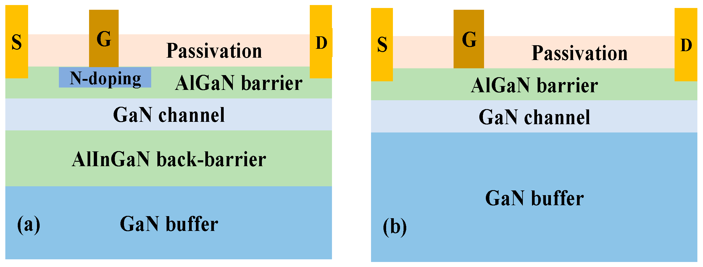
2. Structure and Simulation Models

Figure 1a and 1b show the schematic structures of the GaN HEMT with an Al0.7In0.15Ga0.15N back-barrier layer and an N-type locally doped barrier layer (BD-HEMT) and the conventional GaN HEMT (C-HEMT), respectively. In BD-HEMT, the N-type locally doped barrier layer has a doping concentration of 1 × 1018 cm−3 [13], a thickness of 20 nm, and a length of 2.1 μm. The source-to-gate spacing is set to 1.5 μm, the gate-to-drain spacing to 2.4 μm, and the gate length to 1.1 μm. Both the source and drain regions are heavily doped with an N-type concentration of 1 × 1020 cm−3 to ensure good ohmic contact. The GaN buffer layer is background-doped at 1 × 1016 cm−3, and the gate work function is set to 5.2 eV [14]. All other structural parameters of BD-HEMT are identical to those of the C-HEMT, as listed in Table 1.
The simulation results of the device characteristics were obtained using the Sentaurus-TCAD. In the simulations, several physical models were employed, including the hydrodynamic model, the doping-dependent and high-field-dependent mobility model, and the Shockley–Read–Hall (SRH) recombination model [15,16,17,18]. To validate the accuracy of these models, the simulated transfer characteristics were compared with experimental measurement data [19], as shown in Figure 2. The results demonstrate excellent agreement between the simulated and measured transfer and output characteristics.

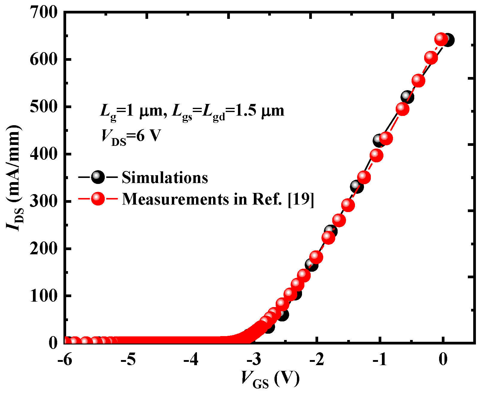
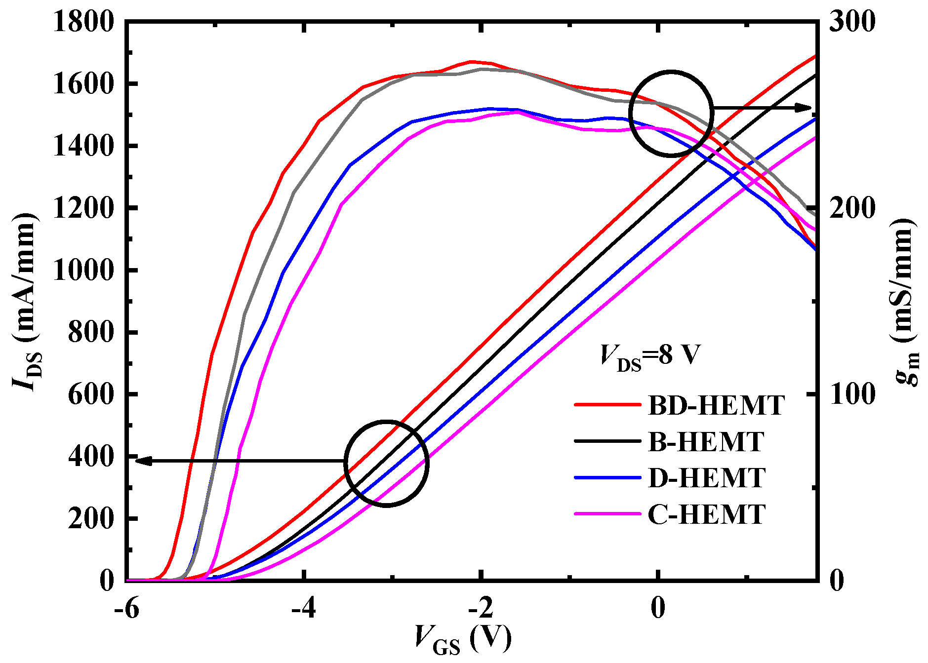
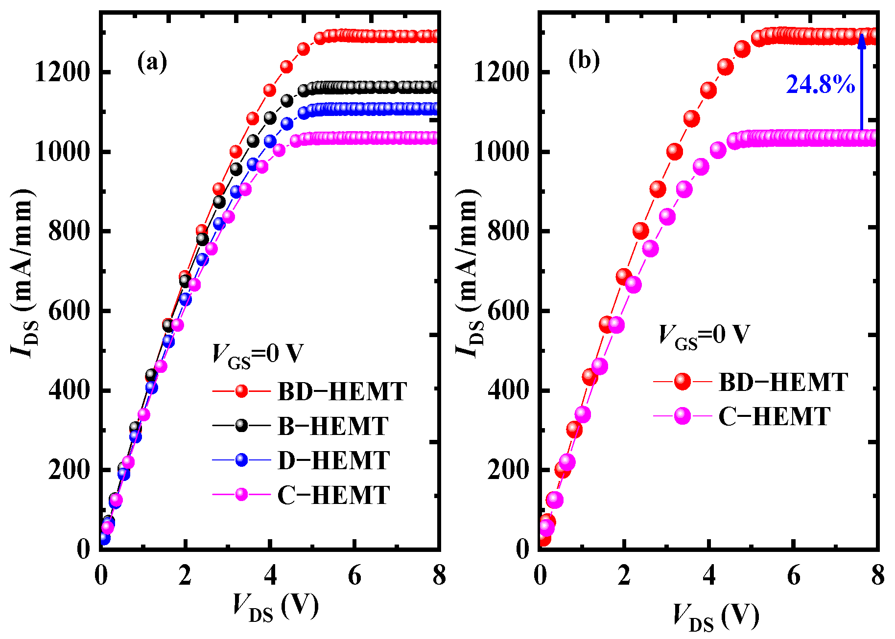
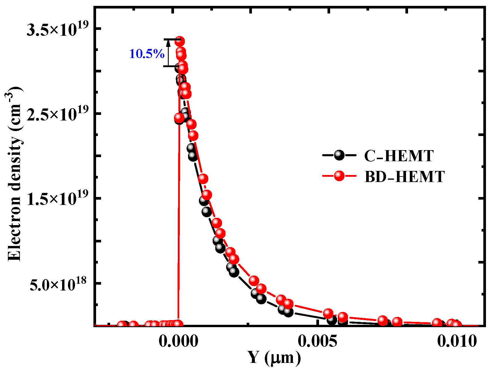
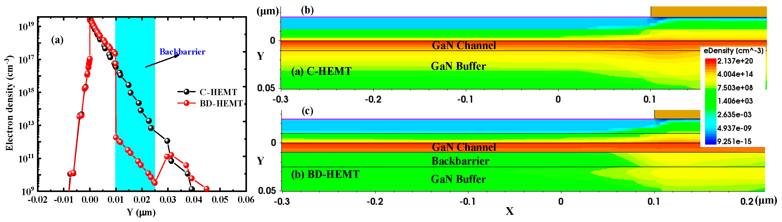
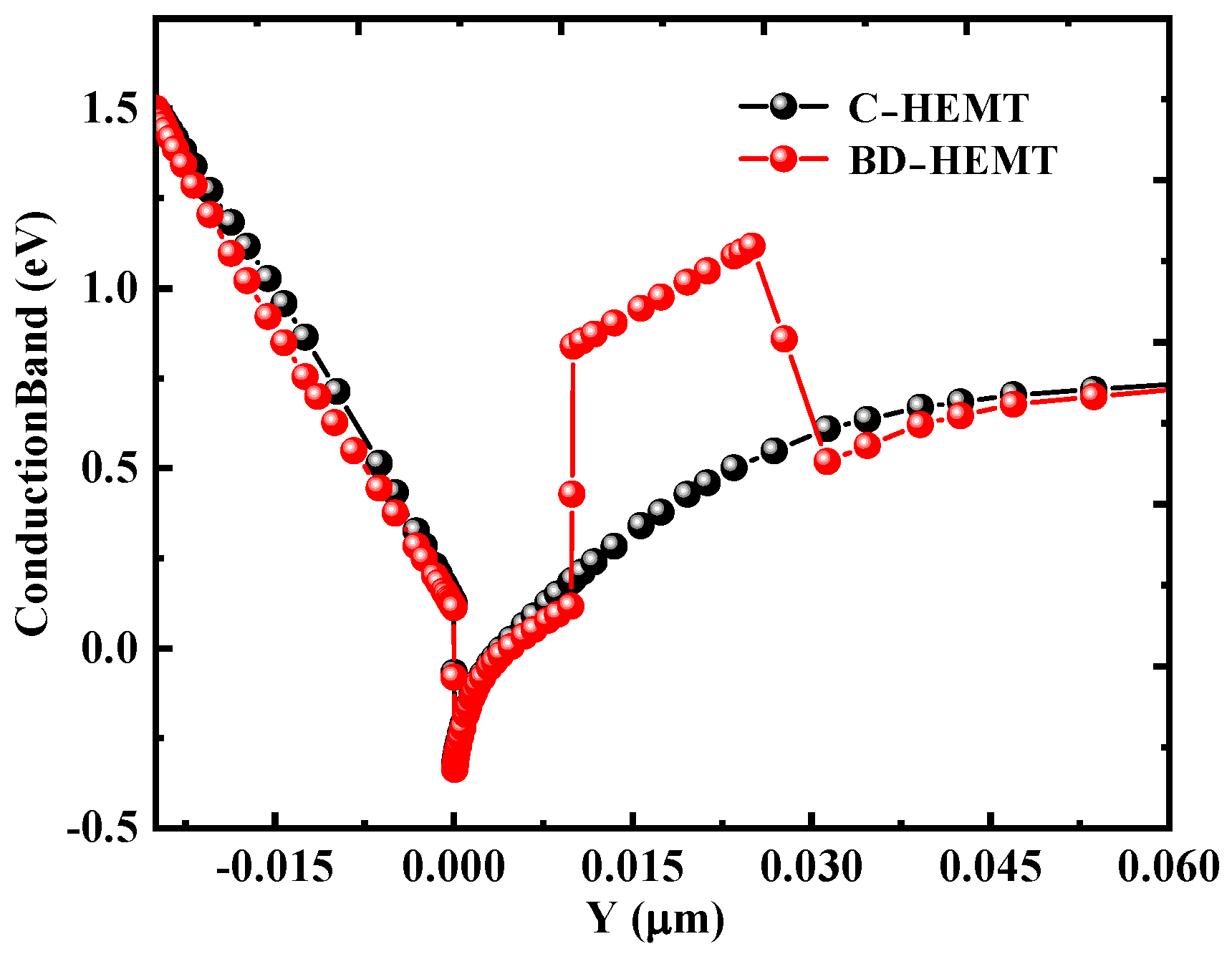
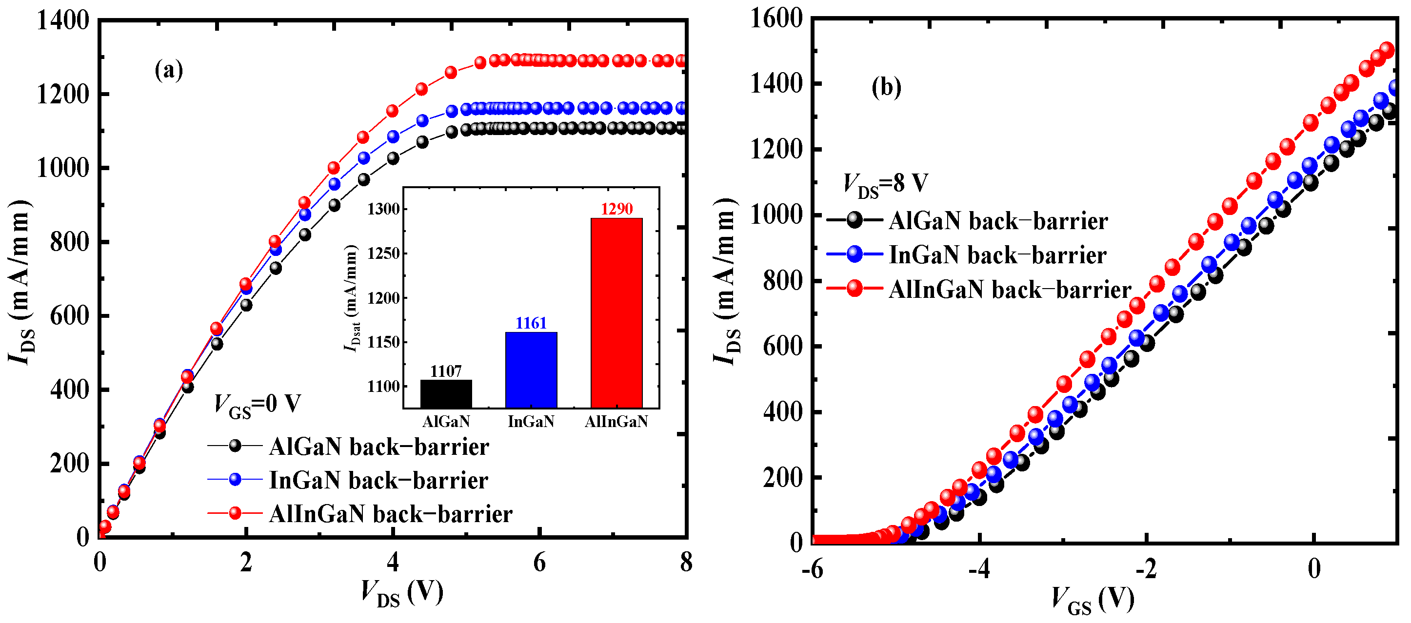
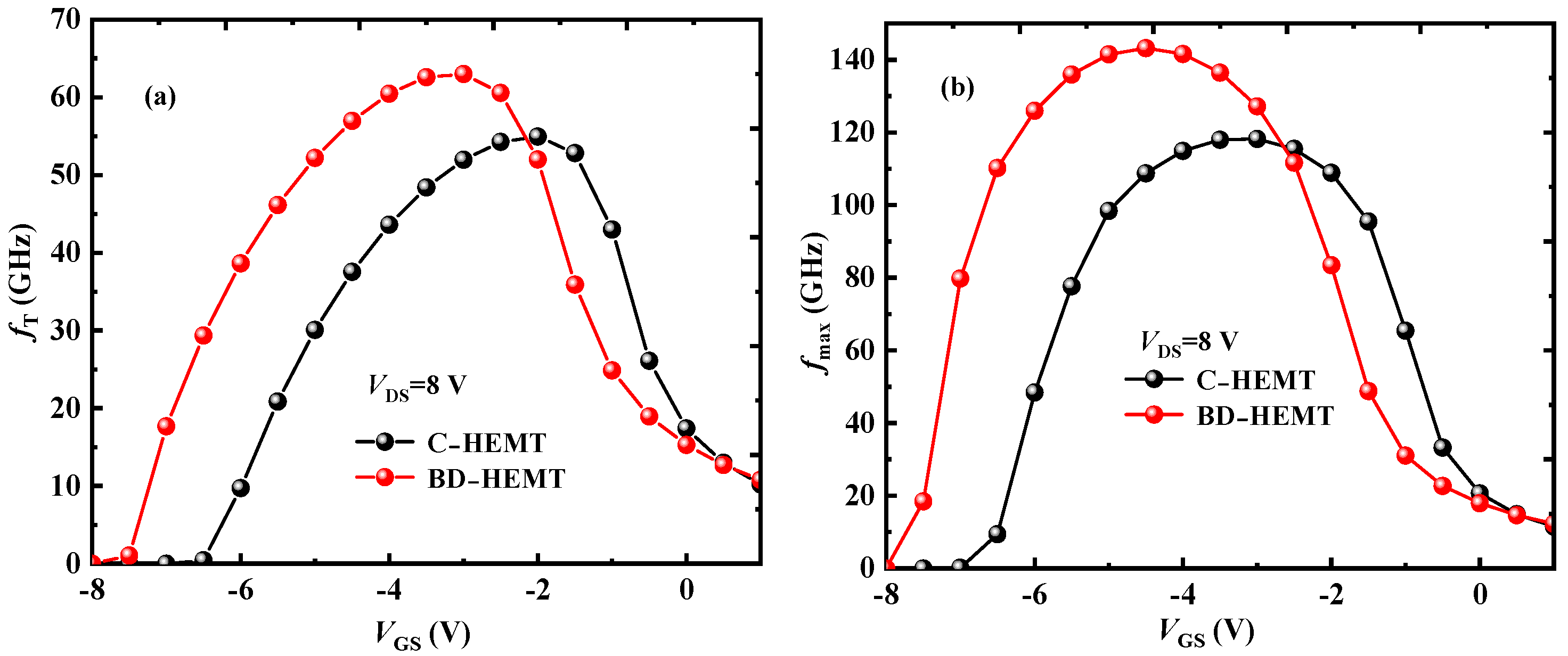
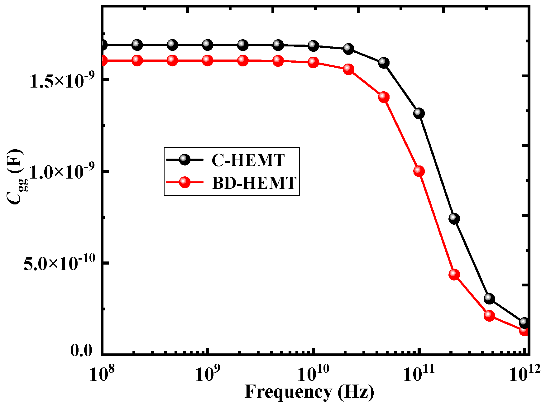
3. Results and Discussion

The mole fraction of Al0.7In0.15Ga0.15N back-barrier is taken from reference [20]. In the simulation, the drain voltage (VDS) was fixed at 8 V, while the gate voltage (VGS) was swept from −6 V to 1 V.
Figure 3 presents the transfer characteristics of BD-HEMT, B-HEMT (with only the AlInGaN back-barrier layer), D-HEMT (with only the locally doped AlGaN barrier layer), and C-HEMT. As evident from Figure 3, the highest drain current (IDS) and transconductance (gm) are achieved for BD-HEMT. Figure 4 displays the extracted maximum drain current (IDmax) and maximum transconductance (gmax) values from Figure 3. At VGS = 1 V, the BD-HEMT achieves an IDmax of 1522 mA/mm, representing an 18.4% improvement compared to the C-HEMT’s 1285 mA/mm. Furthermore, BD-HEMT exhibits a gmax of 278 mS/mm, which is 10.4% higher than the C-HEMT’s 251 mS/mm. DIBL is a key parameter for evaluating the electrostatic integrity of HEMTs. It quantifies the threshold voltage shift induced by variations in the drain voltage. A lower DIBL value indicates superior gate control and enhanced immunity to short-channel effects [21]. The DIBL of 84 mV/V for BD-HEMT is obtained using 87 mV/V for C-HEMT. Therefore, BD-HEMT shows a better gate control ability.
Figure 5a shows the output characteristics of BD–HEMT, B–HEMT, D–HEMT, C–HEMT, and C–HEMT, with VDS ranging from 0 V to 8 V at VGS values of 0 V. The results demonstrate that the incorporation of both the AlInGaN back-barrier layer and locally doped AlGaN barrier layer leads to a significant increase in IDS. At VGS = 0 V, BD–HEMT achieves a saturation drain current (IDsat) of 1290 mA/mm, representing a 24.8% enhancement compared to the C–HEMT’s 1035 mA/mm, as shown in Figure 5b.
To investigate the mechanism behind the improved IDsat and gmax in BD-HEMT, the electron concentration distribution in the channel was analyzed. Figure 6 presents the electron concentration profiles of BD-HEMT and C-HEMT. The results clearly show a significant increase in electron concentration within the BD-HEMT channel, with a 10.5% higher peak electron concentration compared to C-HEMT. This enhancement is attributed to the effective electron confinement in the GaN channel by the AlInGaN back-barrier layer, as demonstrated in Figure 7a. As clearly shown in the figure, the AlInGaN back-barrier layer induces a rapid decline in electron density beneath the BD-HEMT channel. In stark contrast, the C–HEMT exhibits significant electron spillage into the GaN buffer layer due to the absence of such confinement mechanism. Figure 7b,c present the two-dimensional distribution of electron concentration in BD–HEMT and C–HEMT devices. Although electrons in C–HEMT are primarily distributed in the channel, noticeable electron leakage into the GaN buffer layer is observed, as shown in Figure 7b. In contrast, electrons are effectively confined within the channel region without forming any parasitic conduction path in the GaN buffer layer for BD–HEMT, as shown in Figure 7c. These findings confirm that the incorporation of the AlInGaN back-barrier layer significantly enhances the electron concentration in the GaN channel, thereby improving the device’s DC performance characteristics.
The AlInGaN back–barrier effectively confines electrons within the channel by introducing a conduction band offset at the GaN/AlInGaN interface. This offset forms an additional energy barrier that significantly suppresses electron leakage into the buffer layer. Figure 8 presents the conduction band diagrams of both BD–HEMT and C–HEMT. The results clearly reveal a newly formed energy band discontinuity of 0.57 eV at the interface between the GaN channel layer and the AlInGaN back-barrier. To leak from the GaN channel into the GaN buffer layer, electrons must overcome this substantially increased energy barrier [11]. Thus, the AlInGaN back–barrier layer effectively suppresses electron overflow from the channel, thereby enhancing the electron concentration within the channel.
Additionally, the N-type locally doped barrier layer supplies extra electrons to the channel, thereby further increasing the electron concentration in the channel region. Figure 9 presents the electron concentration profiles along the AlGaN/GaN interface for both BD-HEMT and C-HEMT. As clearly illustrated, the electron concentration in BD-HEMT is significantly higher than that in C-HEMT across the entire measured range, with a particularly pronounced increase observed directly beneath the N-type locally doped barrier layer. This clearly demonstrates that the N-type locally doped barrier layer effectively injects additional electrons into the GaN channel, thereby further enhancing both the IDsat and gmax in BD-HEMT devices.
Figure 10 shows the effect of the same thickness of Al0.05Ga0.95N, In0.1Ga0.9N and AlInGaN back barrier on the output characteristics of the GaN HEMT. The results show that the device with the AlInGaN back-barrier has achieved better IDS.
Figure 11 presents the variations of cutoff frequency (fT) and maximum oscillation frequency (fmax) with VGS. As clearly demonstrated in the figures, BD-HEMT exhibits significant improvements in fT and fmax. The maximum fT of BD-HEMT and C-HEMT is 63 GHz and 55 GHz, respectively, and the maximum fmax is 143 GHz and 118 GHz, respectively. Compared with C-HEMT, the maximum fT and fmax of BD-HEMT increased by 14.8% and 21.2%, respectively.
To explain the reasons for the increase in fT and fmax of the device after introducing the AlInGaN back-barrier layer and locally doped AlGaN barrier layer, the variation of the gate capacitance (Cgg) with frequency was simulated and studied, as shown in Figure 12. The simulation results show that, compared with C-HEMT, the Cgg of BD-HEMT is smaller throughout the entire frequency range. Therefore, BD-HEMT achieves higher fT and fmax [13]. Furthermore, the introduction of the locally doped AlGaN barrier layer increases the number of electrons beneath the gate-source and gate-drain regions, thereby resulting in a decrease in the gate-source and gate-drain resistances, which further increases fT and fmax.

4. Conclusions

In this paper, the DC and RF characteristics of BD-HEMT are studied through simulation. The simulation results show that the DC and RF characteristics of the device are significantly improved after the introduction of AlInGaN back-barrier layer and N-type locally doped AlGaN barrier layer. Compared with C-HEMT, BD-HEMT improves in IDsat by 24.8%, gmax by 10.4%, maximum fT and fmax by 14.8% and 21.2%, respectively. This result is caused by the combination of the AlInGaN back-barrier layer and the locally doped AlGaN barrier layer to increase the electron concentration in the channel.

Author Contributions

Conceptualization, L.L., G.Q. and S.S.; validation, J.A.; formal analysis, L.L. and J.A.; investigation, S.S. and L.L.; data curation, X.X.; writing—original draft preparation, S.S. and G.Q.; writing—review and editing, X.X. and S.S.; funding acquisition, S.S. All authors have read and agreed to the published version of the manuscript.

Funding

This work was supported by the Science and Technology Innovation Key R&D Program of Chongqing under Grant 2024TIAD-STX0009, the National Natural Science Foundation of China (No. 62204094), the Henan Province Joint Fund Project of Science and Technology under Grant 225200810085, the Henan Key Laboratory of Smart Lighting Grant 2023KF07, the Zhumadian City Science and Technology Innovation Youth Project under Grant QNZX202325, the Young Backbone Teacher of Project of Henan Province under Grant 2024GGJS128, the and Young Backbone Teacher of Project of Huanghuai University.

Data Availability Statement

Data are contained within the article.

Conflicts of Interest

The authors declare no conflicts of interest.

References

  1. Mounika, B.; Ajayan, J.; Bhattacharya, S.; Nirmal, D.; Dwivedi, A.K. LG = 50 nm T-gated and Fe-doped double quantum well GaN–HEMT on SiC wafer with graded AlGaN barrier for future power electronics applications. J. Sci. Adv. Mater. Devices 2024, 9, 100795. [Google Scholar] [CrossRef]
  2. Sun, S.X.; Zhang, Y.J.; Si, Y.H.; Xiong, J.; Luo, X.R. Improvement of Breakdown Characteristic for a Novel GaN HEMT with Enhanced Resistance Single-Event Transient Effect. J. Electron. Mater. 2025, 54, 784–791. [Google Scholar] [CrossRef]
  3. Mounika, B.; Ajayan, J.; Bhattacharya, S. Investigation on impact of AlxGa1-xN and InGaN back barriers and source-drain spacing on the DC/RF performance of Fe-doped recessed T-gated AlN/GaN HEMT on SiC wafer for future RF power applications. Micro Nanostruct. 2023, 175, 207504. [Google Scholar] [CrossRef]
  4. Haziq, M.; Falina, S.; Manaf, A.A.; Kawarada, H.; Syamsul, M. Challenges and Opportunities for High-Power and High-Frequency AlGaN/GaN High-Electron-Mobility Transistor (HEMT) Applications: A Review. Micromachines 2022, 13, 2133. [Google Scholar] [CrossRef]
  5. Wu, N.T.; Xing, Z.H.; Li, S.J.; Luo, L.; Zeng, F.Y.; Li, G.Q. GaN-based power high-electron-mobility transistors on Si substrates: From materials to devices. Semicond. Sci. Technol. 2023, 38, 063002. [Google Scholar] [CrossRef]
  6. Han, L.; Tang, X.; Wang, Z.; Gong, W.; Zhai, R.; Jia, Z.; Zhang, W. Research Progress and Development Prospects of Enhanced GaN HEMTs. Crystals 2023, 13, 911. [Google Scholar] [CrossRef]
  7. Zhang, H.C.; Wang, H.; Zhang, M.S.; Zuo, C.J.; Yang, L.; Yang, Y.S.; Ye, Y.K.; Qian, H.T.; Zhang, X.C.; Pei, Y.; et al. 2DEG-Concentration-Modulated High-Power-Density AlGaN/GaN RF HEMTs. IEEE Electron. Device Lett. 2024, 45, 1157–1160. [Google Scholar] [CrossRef]
  8. Sinha, K.; Dubey, S.K.; Islam, A. Study of high Al fraction in AlGaN barrier HEMT and GaN and InGaN channel HEMT with In0.17Al0.83N barrier. Microsyst. Technol. 2020, 26, 2145–2158. [Google Scholar] [CrossRef]
  9. Purnachandra Rao, G.; Lenka, T.R.; Boukortt, N.E.I.; Sadaf, S.M.; Nguyen, H.P.T. Investigation of performance enhancement of a recessed gate field-plated AlGaN/AlN/GaN nano-HEMT on β-Ga2O3 substrate with variation of AlN spacer layer thickness. J. Mater. Sci. Mater. Electron. 2023, 34, 1442. [Google Scholar]
  10. Liu, H.X.; Huang, H.M.; Wang, K.; Xie, Z.J.; Wang, H. Impact of composition and thickness of step-graded AlGaN barrier in AlGaN/GaN heterostructures. Mater. Sci. Eng. B 2024, 178, 108460. [Google Scholar] [CrossRef]
  11. Wang, H.L.; Yang, P.; Xu, K.; Duan, X.Y.; Sun, S.X. The AlInGaN back barrier effect on DC characteristics of AlGaN/GaN high electron mobility transistor. Int. J. Mod. Phys. B 2019, 33, 1950190. [Google Scholar] [CrossRef]
  12. Xiong, J.; Xie, X.T.; Wei, J.; Sun, S.X.; Luo, X.R. Improvement of Single Event Transient Effects for a Novel AlGaN/GaN High Electron-Mobility Transistor with a P-GaN Buried Layer and a Locally Doped Barrier Layer. Micromachines 2024, 15, 1158. [Google Scholar] [CrossRef]
  13. Fu, W.L.; Xu, Y.H.; Yan, B.; Zhang, B.; Xu, R.M. Numerical simulation of local doped barrier layer AlGaN/GaN HEMTs. Superlattices Microstruct. 2013, 60, 443–452. [Google Scholar] [CrossRef]
  14. Jia, Y.; Wang, Q.; Chen, C.; Feng, C.; Li, W.; Jiang, L.; Xiao, H.; Wang, Q.; Xu, X.; Wang, X. Simulation of a Parallel Dual-Metal-Gate Structure forAlGaN/GaN High-Electron-Mobility Transistor High-Linearity Applications. Phys. Status Solidi A 2021, 218, 2100151. [Google Scholar] [CrossRef]
  15. Bindhu, S.K.H.; Verma, Y.K.; Dheep, G.R. DC and RF performance analysis of scaled AlInN/GaN HEMTs with single and double-gate structures. Micro Nanostruct. 2025, 205, 208173. [Google Scholar] [CrossRef]
  16. Akshaykranth, A.; Ajayan, J.; Bhattacharya, S.; Nirmal, D.; Paramasivam, S.; Gatto, G.; Kumar, A. Aggressively scaled T-Gated GaN-on-silicon RF power HEMT featuring step graded SRL-AlGaN buffer for next generation broad band power amplifiers. Results Eng. 2025, 25, 104151. [Google Scholar] [CrossRef]
  17. Feng, B.M.; Wang, Y.; Yu, C.H.; Guo, H.M. A novel p-GaN HEMT with superjunction silicon substrate for improved current collapse. Micro Nanostruct. 2025, 201, 208102. [Google Scholar] [CrossRef]
  18. Sun, S.X.; Xie, X.T.; Zhang, P.F.; Zhao, Z.J.; Wei, J.; Luo, X.R. Improvement of single event transients effect for a novel AlGaN/GaN HEMT with enhanced breakdown voltage. J. Sci. Adv. Mater. Devices 2024, 9, 100692. [Google Scholar] [CrossRef]
  19. Huang, J.; Li, M.; Tang, C.W.; Lau, K.M. Lg = 100 nm T-shaped gate AlGaN/GaN HEMTs on Si substrates with non-planar source/drain regrowth of highly-doped n+-GaN layer by MOCVD. Chin. Phys. B 2014, 23, 128102. [Google Scholar] [CrossRef]
  20. Mojaver, H.R.; Gosselin, J.L.; Valizadeh, P. Use of a bilayer lattice-matched AlInGaN barrier for improving the channel carrier confinement of enhancement-mode AlInGaN/GaN hetero-structure field-effect transistors. J. Appl. Phys. 2017, 121, 244502. [Google Scholar] [CrossRef]
  21. Adak, S.; Sarkar, A.; Swain, S.; Pardeshi, H.; Pat, S.K.; Sarkar, C.K. High performance AlInN/AlN/GaN p-GaN back barrier Gate-Recessed Enhancement-Mode HEMT. Superlattices Microstruct. 2014, 75, 347–357. [Google Scholar] [CrossRef]
Figure 1. Schematic diagrams of (a) BD-HEMT and (b) C-HEMT.
Micromachines 16 00779 g001
Figure 2. Comparison of the simulated and experimental transfer characteristics.
Micromachines 16 00779 g002
Figure 3. Transfer characteristics of BD–HEMT, B–HEMT, D–HEMT, and C–HEMT.
Micromachines 16 00779 g003
Figure 4. IDmax and gmax of BD–HEMT and C–HEMT.
Micromachines 16 00779 g004
Figure 5. (a) Output characteristics for different devices. (b) Output characteristics for BD–HEMT and C–HEMT.
Micromachines 16 00779 g005
Figure 6. Electron distribution of BD–HEMT and C–HEMT.
Micromachines 16 00779 g006
Figure 7. (a) Electron distribution of BD–HEMT and C–HEMT; two–dimensional distribution of electron concentration for (b) C–HEMT and (c) BD–HEMT.
Micromachines 16 00779 g007
Figure 8. Conduction band diagrams of BD-HEMT and C-HEMT.
Micromachines 16 00779 g008
Figure 9. Electron concentration distribution along the GaN channel for BD-HEMT and C-HEMT.
Micromachines 16 00779 g009
Figure 10. (a) Output and (b) transfer characteristics for structure with the different back-barrier materials.
Micromachines 16 00779 g010
Figure 11. (a) fT and (b) fmax of BD-HEMT and C-HEMT.
Micromachines 16 00779 g011
Figure 12. Variation of Cgg for BD-HEMT and C-HEMT.
Micromachines 16 00779 g012
Table 1. Structural parameters of BD-HEMT.
LayerValue
Passivation layer50 nm
N-type locally doped barrier layer20 nm
Al0.3Ga0.7N barrier layer25 nm
GaN channel layer10 nm
Al0.7In0.15Ga0.15N back-barrier layer15 nm
GaN buffer layer1.5 μm
Disclaimer/Publisher’s Note: The statements, opinions and data contained in all publications are solely those of the individual author(s) and contributor(s) and not of MDPI and/or the editor(s). MDPI and/or the editor(s) disclaim responsibility for any injury to people or property resulting from any ideas, methods, instructions or products referred to in the content.

