
A 40 GHz High-Image-Rejection LNA with a Switchable Transformer-Based Notch Filter in 65 nm CMOS

Abstract
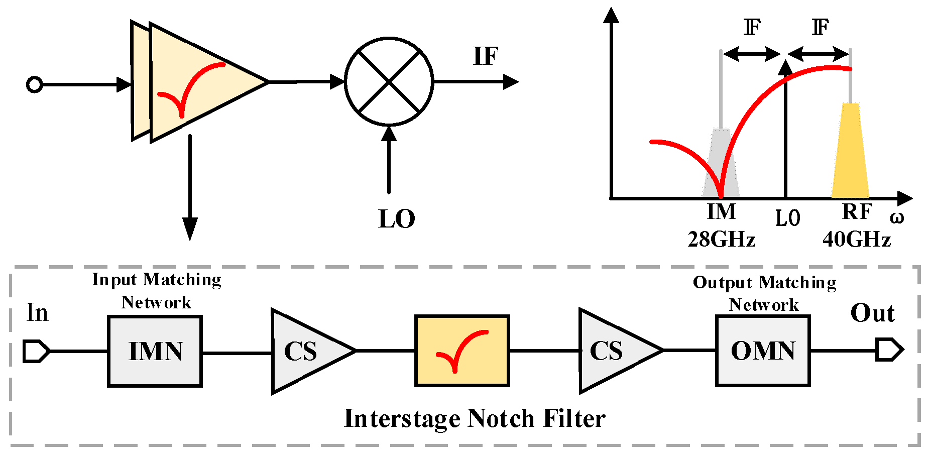
1. Introduction
2. Analysis of the Switchable Transformer-Based Notch Filter
2.1. Pole-Zero Analysis
2.2. Quality Factor at Zero and IRR of the Notch Filter
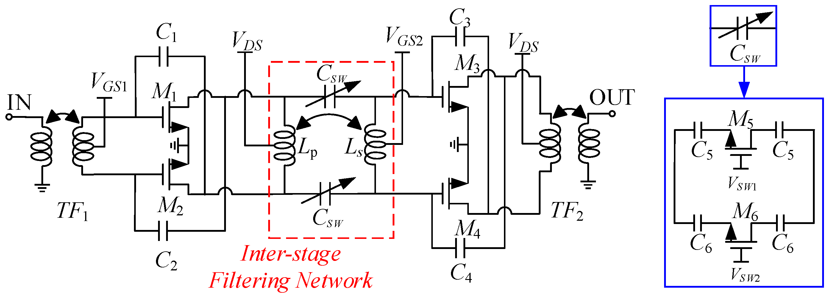
3. The 40 GHz LNA Circuit Design
3.1. Overall Circuit Design
3.2. Switched Capacitor Array
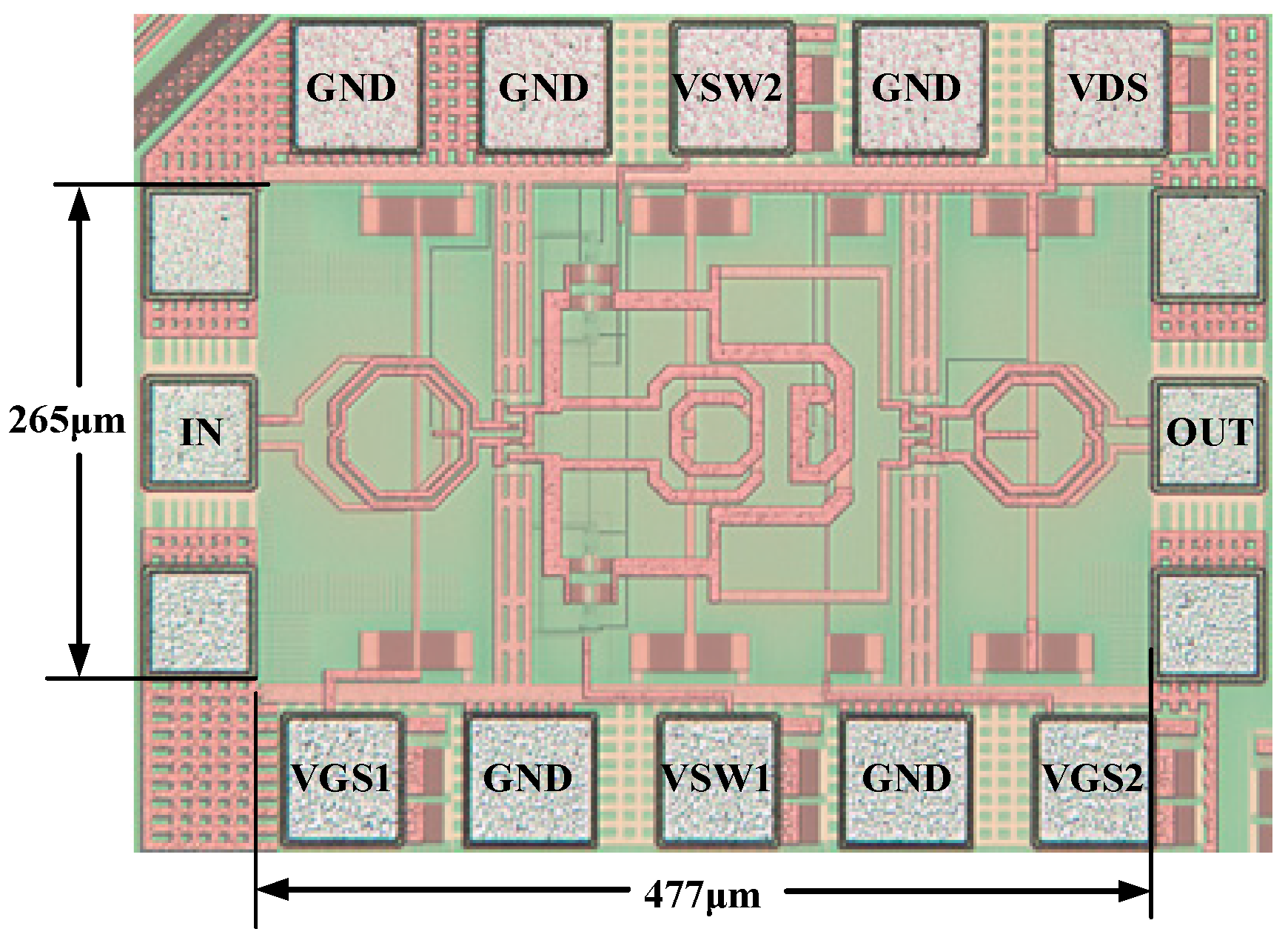
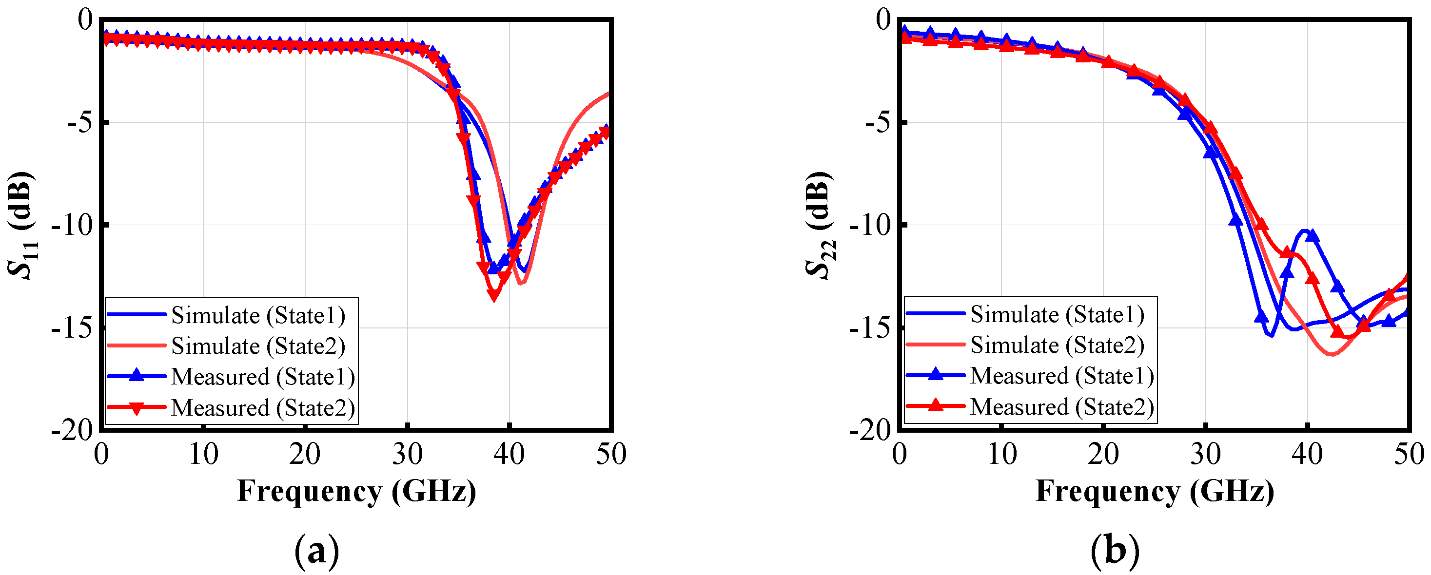
4. Measurement Results
5. Conclusions
Author Contributions
Funding
Data Availability Statement
Conflicts of Interest
References
- Kim, D.; Im, D. A 2.4 GHz reconfigurable cascode/folded-cascode inductive source degenerated LNA with enhanced OP1dB and OIP3 over gain reduction. IEEE Trans. Circuits Syst. II Express Briefs 2023, 70, 1831–1835. [Google Scholar] [CrossRef]
- Chang, J.F.; Lin, Y.S. A 13.7-mW 21–29-GHz CMOS LNA with 21.6-dB gain and 2.74-dB NF for 28-GHz 5G systems. IEEE Microw. Wirel. Compon. Lett. 2021, 32, 137–140. [Google Scholar] [CrossRef]
- Cui, B.; Long, J.R. A 1.7-dB minimum NF, 22–32-GHz low-noise feedback amplifier with multistage noise matching in 22-nm FD-SOI CMOS. IEEE J. Solid-State Circuits 2020, 55, 1239–1248. [Google Scholar] [CrossRef]
- Hu, Y.; Chi, T. A 27–46-GHz low-noise amplifier with dual-resonant input matching and a transformer-based broadband output network. IEEE Microw. Wirel. Compon. Lett. 2021, 31, 725–728. [Google Scholar] [CrossRef]
- Chen, X.; Li, L.; Cheng, D.; Fan, X. A 22–34 GHz Wide-Band Low Noise Amplifier with 22 dB Gain and 4 dB NF. In Proceedings of the IEEE MTT-S International Wireless Symposium (IWS), Nanjing, China, 23–26 May 2021; pp. 1–3. [Google Scholar]
- Lin, Y.S.; Lan, K.S. Design and analysis of a wideband K/Ka-band CMOS LNA using coupled-TL feedback. IEEE Trans. Circuits Syst. II Express Briefs 2022, 70, 1851–1855. [Google Scholar] [CrossRef]
- Alshammary, H.; Hill, C.; Hamza, A.; Buckwalter, J.F. A code-domain RF signal processing front end with high self-interference rejection and power handling for simultaneous transmit and receive. IEEE J. Solid-State Circuits 2020, 55, 1199–1211. [Google Scholar] [CrossRef]
- Bai, H.; Hao, L.; Wang, D.; Zhang, N.; Gao, K.; He, J.; Zhou, J.; Liu, J.; Liao, H. A Sub-6 GHz Wideband Transceiver Chipset With Calibration-Friendly Harmonic Rejection RF Front-Ends. IEEE Trans. Microw. Theory Tech. 2025, 73, 2084–2096. [Google Scholar] [CrossRef]
- Gebhard, A.; Sadjina, S.; Tertinek, S.; Dufrêne, K.; Pretl, H.; Huemer, M. A harmonic rejection strategy for 25% duty-cycle IQ-mixers using digital-to-time converters. IEEE Trans. Circuits Syst. II Express Briefs 2019, 67, 1229–1233. [Google Scholar] [CrossRef]
- Kwon, K.; Kim, S.; Son, K.Y. A hybrid transformer-based CMOS duplexer with a single-ended notch-filtered LNA for highly integrated tunable RF front-ends. IEEE Microw. Wirel. Compon. Lett. 2018, 28, 1032–1034. [Google Scholar] [CrossRef]
- Li, Y.; Li, X.; Huang, Z.; Tan, T.; Chen, D.; Cao, C.; Qi, Z. A novel low-power notch-enhanced active filter for ultrawideband interferer rejected LNA. IEEE Trans. Microw. Theory Tech. 2021, 69, 1684–1697. [Google Scholar] [CrossRef]
- Zhang, J.; Zhao, D.; You, X. A CMOS LNA with transformer-based integrated notch filter for Ku-band satellite communications. In Proceedings of the IEEE MTT-S International Microwave Symposium, Atlanta, GA, USA, 7–25 June 2021; pp. 592–594. [Google Scholar]
- Bardeh, M.G.; Fu, J.; Naseh, N.; Paramesh, J.; Entesari, K. A mm-wave wideband/reconfigurable LNA using a 3-winding transformer load in 22-nm CMOS FDSOI. In Proceedings of the IEEE Radio Frequency Integrated Circuits Symposium (RFIC), San Diego, CA, USA, 11–13 June 2023; pp. 121–124. [Google Scholar]
- Gao, L.; Ma, Q.; Rebeiz, G.M. A 20–44-GHz image-rejection receiver with >75-dB image-rejection ratio in 22-nm CMOS FD-SOI for 5G applications. IEEE Trans. Microw. Theory Tech. 2020, 68, 2823–2832. [Google Scholar] [CrossRef]
- Chen, Z.; Gao, H.; Leenaerts, D.; Milosevic, D.; Baltus, P. A 29–37 GHz BiCMOS low-noise amplifier with 28.5 dB peak gain and 3.1–4.1 dB NF. In Proceedings of the 2018 IEEE Radio Frequency Integrated Circuits Symposium, Philadelphia, PA, USA, 10–12 June 2018; pp. 288–291. [Google Scholar]
- Li, H.Y.; Xu, J.X.; Gao, L.; Xue, Q.; Zhang, X.Y. 24–35 GHz filtering LNA and filtering switch using compact mixed magnetic-electric coupling circuit in 28-nm bulk CMOS. IEEE Trans. Circuits Syst. I Regul. Pap. 2022, 70, 1071–1082. [Google Scholar] [CrossRef]
- Sun, N.Z.; Gao, L.; Li, H.Y.; Xu, J.X.; Zhang, X. A compact millimeter-wave reconfigurable dual-band LNA with image-rejection in 28-nm bulk CMOS for 5G applications. IEEE J. Solid-State Circuits 2024, 59, 3406–3416. [Google Scholar] [CrossRef]
- Wang, X.; Wen, J. Frequency Reconfigurable Pole-Zero Inversion Image Rejection Filter for 5G FR2 Transceivers. IEEE Microw. Wirel. Technol. Lett. 2024, 34, 623–626. [Google Scholar] [CrossRef]
- Wang, Y.; Duan, H.; He, L.; Cheng, D.; Wu, X.; Wang, D.; Reynaert, P.; Li, L. A 39-GHz high image-rejection up-conversion mixer in 65-nm CMOS for 5G communication. IEEE Trans. Circuits Syst. II Express Briefs 2022, 70, 491–495. [Google Scholar] [CrossRef]
- Cheng, D.; Chen, X.; Chen, Q.; Ma, X.; Li, L. A Reconfigurable LNA With Compact Magnetic-Capacitive Coupling Transformer Networks for 5G 28-/39-GHz Applications. IEEE Microw. Wirel. Technol. Lett. 2024, 34, 915–918. [Google Scholar] [CrossRef]
- Liu, B.; Meng, F.; Ma, Z.; Yeo, K.S.; Ma, K. A 28/39 GHz Tri-Mode Frequency-Reconfigurable LNA for Multiband 5G Communications. IEEE Trans. Circuits Syst. II Express Briefs 2024, 71, 4036–4040. [Google Scholar] [CrossRef]
- Fu, J.; Bardeh, M.G.; Paramesh, J.; Entesari, K. A millimeter-wave concurrent LNA in 22-nm CMOS FDSOI for 5G applications. IEEE Trans. Microw. Theory Tech. 2022, 71, 1031–1043. [Google Scholar] [CrossRef]
- Guo, B.; Gong, J. A dual-band low-noise CMOS switched-transconductance mixer with current-source switch driven by sinusoidal LO signals. In Proceedings of the IEEE International Midwest Symposium on Circuits and Systems (MWSCAS), Lansing, MI, USA, 9–11 August 2021; pp. 741–744. [Google Scholar]


| Ref. | Technology | Freq/GHz | Peak Gain/dB | NF/dB | IRR/dB | Power/mW | Area/mm2 | IP1dB/dBm |
|---|---|---|---|---|---|---|---|---|
| [3] | 22-nm FD-SOI | 19–36 | 21.5 | 1.7–2.2 | 6.5 | 17.3 | 0.05 | −24.4~−23.4 |
| 20–36 | 17.9 | 2.1–2.9 | 5.6 | |||||
| [4] | 45-nm RF-SOI | 27–46 | 21.2 | 2.74–3.24 | 21.2 | 25.5 | 0.38 | −21 |
| [13] | 22-nm FD-SOI | 21.6–34.2 | 32 | 2.3 | >30 | 35 | 0.74 | −37.2~−26.6 |
| 21.5–26.5 | 32.4 | 2.7 | ||||||
| 27.5–33 | 33.4 | 2.3 | ||||||
| [14] | 22-nm FD-SOI | 20–44 | 28.5 | 3.3–5 | >75 | 20.5 | 1.8 * | −29.5~−25 |
| [15] | 0.25-μm SiGe | 29–37 | 28.5 | 3.1–4.1 | >30 | 80 | 0.21 * | −22.1 |
| [16] | 28-nm CMOS | 24–35 | 22 | 2.4–3.6 | >25 | 26.8 | 0.13 * | −18.25 |
| [17] | 28-nm CMOS | 23.8–33.5 | 18.1 | 2.5–3.5 | >32.6 | 14 | 0.09 * | −19~−15.1 |
| 34.4–41.4 | 18.9 | 2.8–3.5 | −18.5~−15.2 | |||||
| This work | 65-nm CMOS | 36.3–40.7 | 18 | 4.4–4.9 | 40–53.4 | 25.4 | 0.13 * | −16.2 |
Disclaimer/Publisher’s Note: The statements, opinions and data contained in all publications are solely those of the individual author(s) and contributor(s) and not of MDPI and/or the editor(s). MDPI and/or the editor(s) disclaim responsibility for any injury to people or property resulting from any ideas, methods, instructions or products referred to in the content. |
© 2025 by the authors. Licensee MDPI, Basel, Switzerland. This article is an open access article distributed under the terms and conditions of the Creative Commons Attribution (CC BY) license (https://creativecommons.org/licenses/by/4.0/).
Share and Cite
Guo, Y.; Wen, J. A 40 GHz High-Image-Rejection LNA with a Switchable Transformer-Based Notch Filter in 65 nm CMOS. Micromachines 2025, 16, 676. https://doi.org/10.3390/mi16060676
Guo Y, Wen J. A 40 GHz High-Image-Rejection LNA with a Switchable Transformer-Based Notch Filter in 65 nm CMOS. Micromachines. 2025; 16(6):676. https://doi.org/10.3390/mi16060676
Chicago/Turabian StyleGuo, Yutong, and Jincai Wen. 2025. "A 40 GHz High-Image-Rejection LNA with a Switchable Transformer-Based Notch Filter in 65 nm CMOS" Micromachines 16, no. 6: 676. https://doi.org/10.3390/mi16060676
APA StyleGuo, Y., & Wen, J. (2025). A 40 GHz High-Image-Rejection LNA with a Switchable Transformer-Based Notch Filter in 65 nm CMOS. Micromachines, 16(6), 676. https://doi.org/10.3390/mi16060676