Communication

Design and Implementation of 24-GHz and 48-GHz VCOs Using Noise Filtering Technique in 90-nm CMOS

Department of Electronic Engineering, National Taipei University of Technology, Taipei 10608, Taiwan
*
Author to whom correspondence should be addressed.
Micromachines 2025, 16(6), 682; https://doi.org/10.3390/mi16060682
Submission received: 10 April 2025 / Revised: 18 May 2025 / Accepted: 26 May 2025 / Published: 5 June 2025
(This article belongs to the Special Issue RF and Power Electronic Devices and Applications)

Abstract

:
This work proposes two voltage-controlled oscillators using noise-filtering technique. The first one is a 24-GHz voltage-controlled oscillator, and the second one is based on a push–push architecture with a λ /4 transmission line to further increase the frequency up to 48 GHz. The designs are implemented and verified in a standard 90-nm CMOS process. Typically, the current mirror transistor in the tail current has a nonlinear effect. When the transistor operates in the nonlinear region, noise will be introduced. Therefore, a set of LC filters with a resonant frequency at 2 f 0 are added to the design of this section to filter the noise at 2 f 0 through the capacitor to the ground. The measurement results show that the design of a single oscillator has an oscillation frequency of 24.37 GHz, a tuning range of 6.5%, and a phase noise of −97.19 dBc/Hz @1MHz. The measurement results of the push–push architecture show that the double oscillation frequency is 49.8 GHz, the tuning range is 7.2%, and the phase noise is −80.52 dBc/Hz @1MHz. The chip areas of 24-GHz LC VCO and 48-GHz push–push LC VCO are 0.68 mm × 0.69 mm and 0.7 mm × 0.7 mm, respectively.

1. Introduction

Voltage controlled oscillators (VCOs) play an important role in the design of microwave circuits. Its function is to provide a stable local oscillation (LO) signal. The VCOs are required to have low phase noise, low power consumption, wide tuning range and high output power from the design considerations. In radio frequency (RF) systems, low phase noise can improve the sensitivity and linearity of the receiver, which is crucial for some high-precision RF and digital signal processing systems. However, the tail current in the current mirror transistor has a nonlinear effect, which mixes the second harmonic signal with the fundamental signal to produce a signal with a frequency close to f0. This new signal will shift the 2f0 noise to near the oscillation frequency. In order to reduce phase noise, using LC noise filtering circuit can effectively reduce phase noise [1,2,3] and eliminate the harmonic noise between the current source and the CMOS cross-coupling [4,5,6]. In Section 2 of this paper, we used a set of LC filters with a resonant frequency of 2f0 to filter out the noise at 2f0, through the capacitor to the ground, and reduce the phase noise of the circuit [7].
However, the output signal of a single frequency oscillator is limited by the cut-off frequency of the transistor, which means that the output oscillator signal cannot reach a higher frequency band. Therefore, the push-push architecture used "λ"/4transmission line can improve the output signal limitation of the characteristics of the transistor itself [8], This paper extends the proposed VCO architecture, design a "λ"/4 transmission line combined with an LC voltage-controlled oscillator to implement a Push-Push voltage-controlled oscillator [9,10] and we also discuss how to use the slow wave factor (SWF) equation to design low-attenuation transmission lines [11]. The remainder of this paper is organized as follows. Section 2 describes the design and analysis of the two proposed VCOs. In Section 3, the implementation and measurements of the two VCOs detailed. Finally, Section 4 concludes this paper.

2. Design and Analysis

A standard 90-nm CMOS process offers one poly layer and nine metal layers, as shown in Figure 1. The thicknesses of the top metal layers (M9) and (M8) are 0.85 μm, the thicknesses of the metal layers (M2~7) are all 0.31 μm, while the metal layer (M1) is 0.24 μm. Typically, the M1 layer is also known as the bottom metal layer. Each layer of metal can be connected by Via layers. The poly layer is for the transistor’s gate and thus above the substrate.

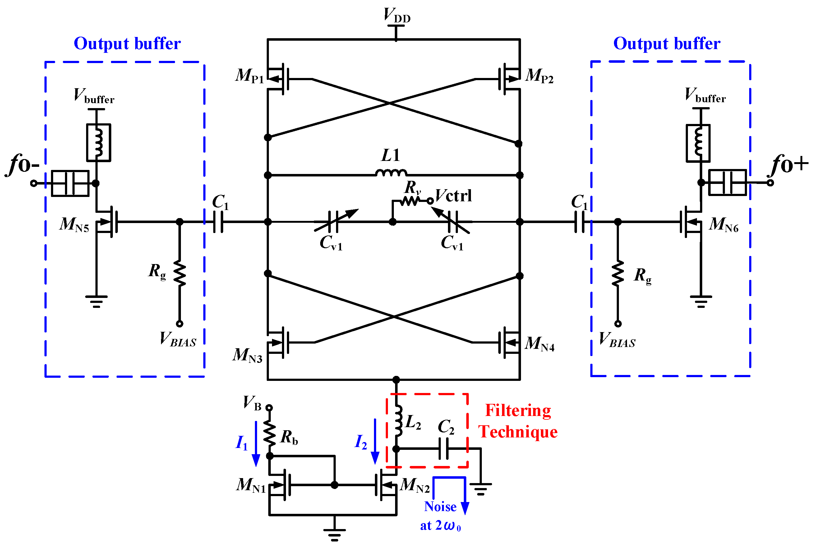
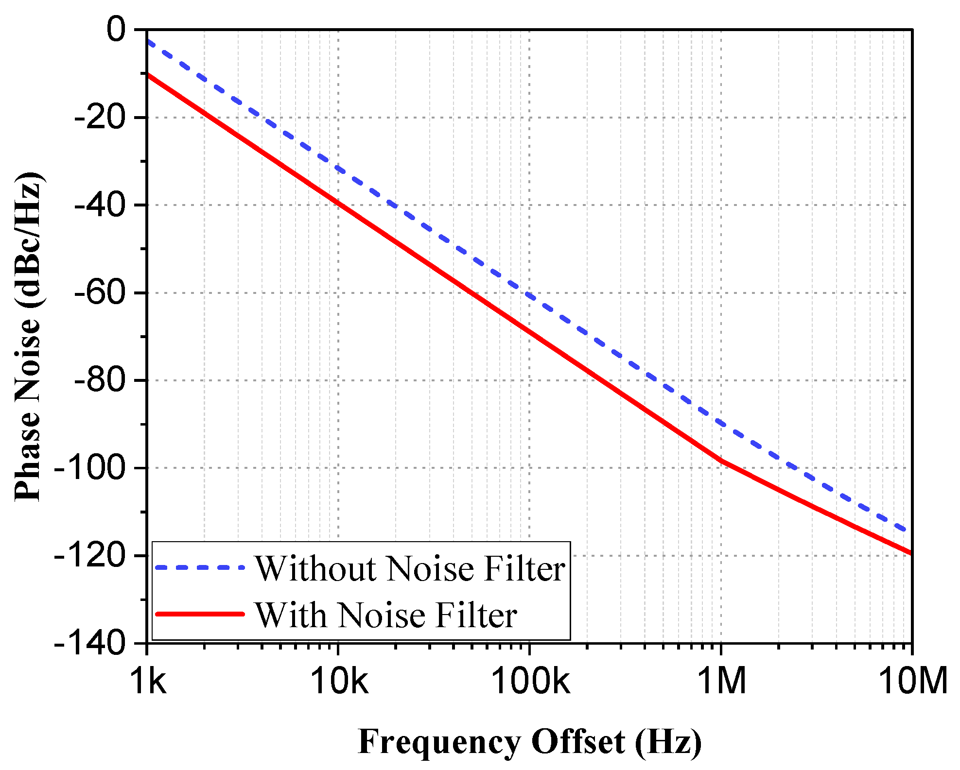
2.1. The Proposed 24-GHz VCO

The schematic of 24 GHz VCO with low phase noise is shown in Figure 2. This circuit is a voltage-controlled oscillator composed of CMOS architecture, MN3, MN4 and Mp1, Mp2 are the cross-couple pair, and the LC resonant cavity is composed of L1 and Cv1. The capacitance change of the variable capacitor in the circuit mainly determines the overall tuning range of the VCO. However, for the circuit to oscillate stably, the negative impedance of the cross-coupled pair needs to offset the positive impedance of the resonant cavity. Therefore, the negative impedance of this voltage-controlled oscillator is created by the cross-coupling of the NMOS and PMOS to the transistor.
The NMOS current mirror can use voltage to limit the size of the tail current, limiting the total power dissipated by the voltage-controlled oscillator. The channel width ratio of the transistors MN1 and MN2 is 16:1. However, the current mirror transistor in the tail current has a nonlinear effect. When the transistor operates in the nonlinear region, noise will be introduced. The second harmonic signal is mixed with the fundamental frequency signal, and the signals are multiplied to produce a signal whose frequency is close to the oscillation frequency, and this new signal will transfer the 2 f 0 noise to near the oscillation frequency, reducing the phase noise of the circuit [4]. Therefore, a set of LC filters with a resonant frequency at 2 f 0 are added to the design of this section to filter the noise at 2 f 0 through the capacitor to the ground. The inductor provides a high impedance of the circuit near the resonant frequency and blocks the passage of the 2f0 signal. The function of the capacitor is to compose a resonant circuit with the inductor [5]. Finally, open-drain buffers MN5 and MN6 are used at the output, and bias Tee is used externally, which can be used to isolate RF and DC signals and enhance the output power.
Figure 3 is the simulated output spectrum of the voltage-controlled oscillator after the implementation of the buffer amplifier. The output oscillation frequency is 23.63 GHz and the output power is 1.58 dBm when Vctrl is 0.6 V, while the frequency range is from 22.8~24.15 GHz, as shown in Figure 4, and the tuning range is 5.45%. Figure 5 shows the simulated results of phase noise after adding a noise filter circuit. The phase noise simulation result is −95.8 dBc/Hz at a carrier offset of 1 MHz. Obviously, the phase noises are improved by about 8.3 dB by adding the noise filter circuit.

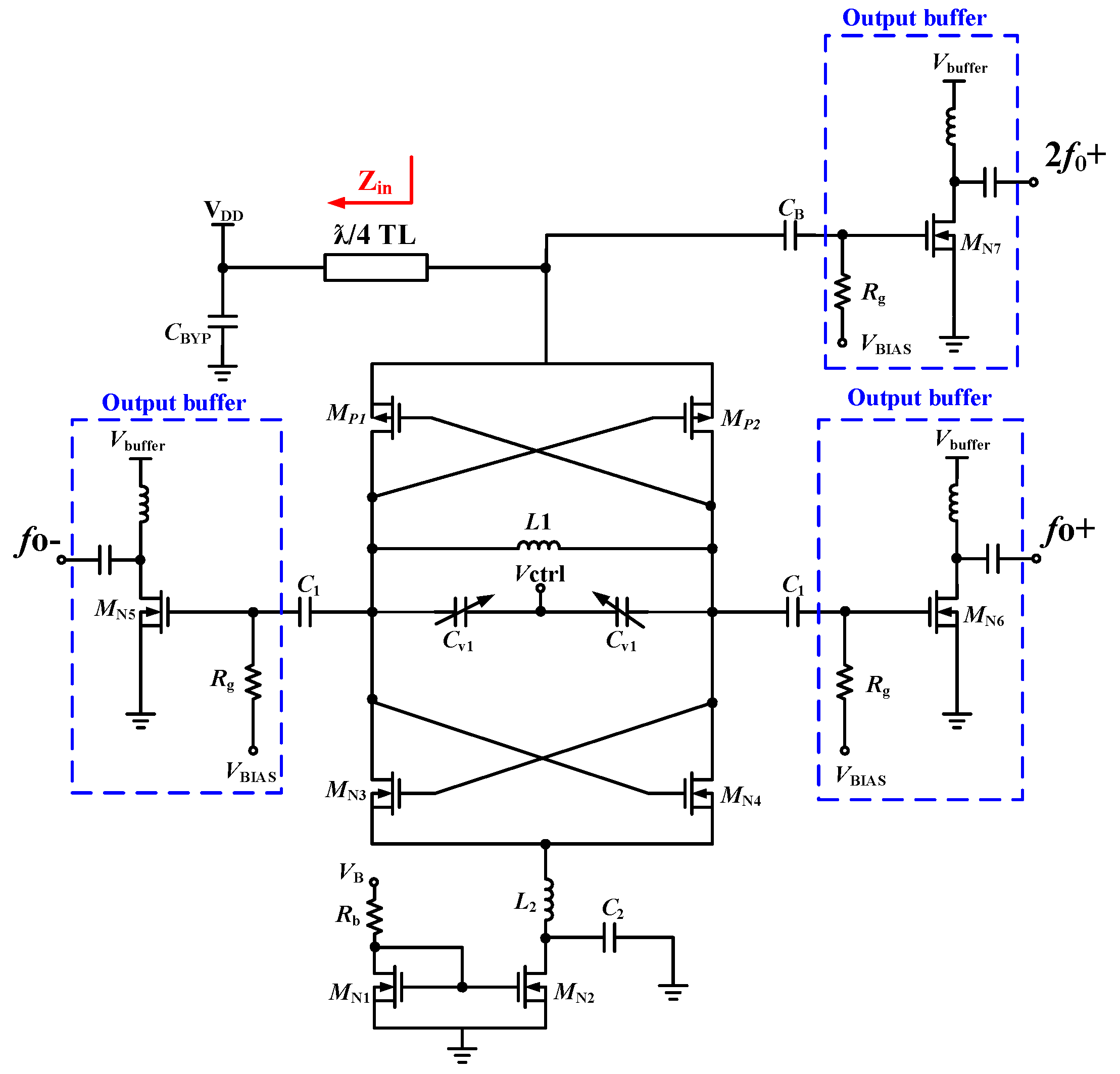
2.2. The Proposed Push–Push 48-GHz VCO

2.2.1. The λ

/4 Transmission Line
With the development of communication systems, low-loss and high slow-wave transmission lines are required for improving circuit performances and miniaturization. In this design, a λ /4 transmission line was combined with an LC voltage-controlled oscillator to implement a push–push VCO. Firstly, the characteristic impedance value of the transmission line must be calculated, as shown in Equation (1).
Z C = Z 0 ( 1 + S 11 ) 2 S 21 2 ( 1 S 11 ) 2 S 21 2
Secondly, according to Equation (2), various electrical characteristics of the transmission line can be extracted. First, we need to extract the effective propagation constant γ of the transmission line, and the effective propagation constant is denoted by γ = α + j β g , where β is the phase constant, α is the attenuation constant, and L is the physical length of the transmission line.
e γ L = 1 S 11 2 + S 21 2 ( 1 + S 11 2 S 21 2 ) 2 ( 2   S 11 ) 2 2   S 21
In the design of transmission lines, the slow wave factor (SWF) plays an important part [8]. The slow wave factor refers to the measurement of the loss and distortion experienced by electromagnetic waves propagating in transmission lines. We can calculate the length of the λ/4 transmission line at 48 GHz to be 672 um based on Equation (3), as shown in Figure 6a. The transmission line is winding according to this length. The slow wave factor and phase after the simulated winding are shown in Figure 6b, and the phase attenuation is shown in Figure 6c.
SWF = β g β 0 = λ 0 λ g = ε r u r ε r

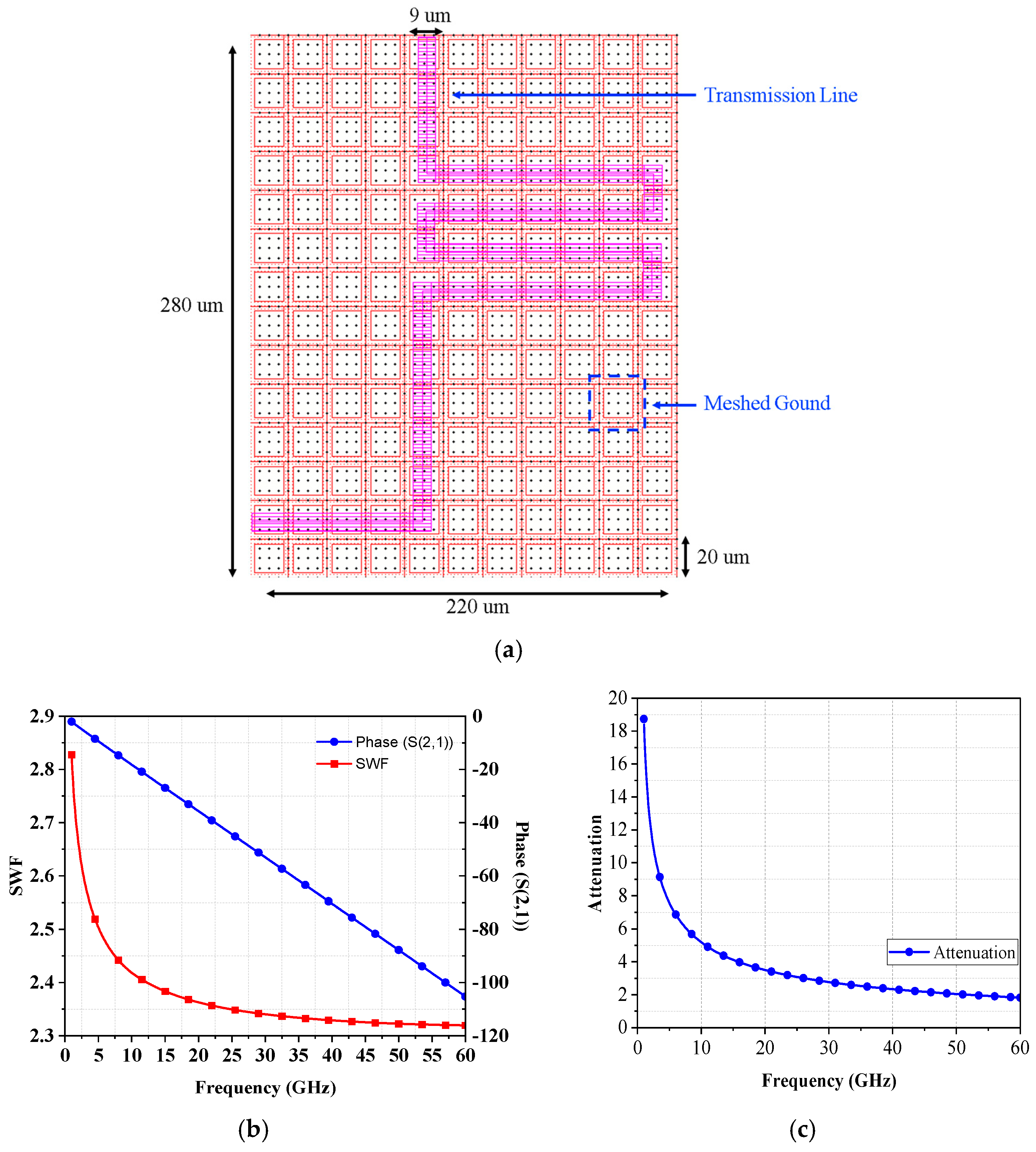
2.2.2. The Push–Push VCO

The schematic of the 48-GHz push–push VCO is shown in Figure 7. This VCO is composed of the cross-couple pair of MN3, MN4, MP1, and MP2, the LC tank of L1 and Cv1, the NMOS current mirror of transistors MN1 and MN2 with a channel width ratio of 16:1, and the LC noise-filtering circuit. In the traditional LC architecture, the inductor used as the resonant circuit can usually be replaced by a λ /2 transmission line. However, this transmission line is the state of one wavelength, so the oscillation frequency at 2f0 is in phase and multiplies, f0 is the differential signal cancellation, and an oscillation signal of 2f0 is generated; this is extracted through the AC coupling capacitor CB through open-drain buffers MN7 to output a double-frequency oscillation signal, and λ /4 of the transmission line in the circuit is in the 2f0 state. It functions as an RF Choke in the circuit to isolate RF signals. Zin represents the input impedance of the transmission line. The load impedance ZL in Equation (4) is 0, Z0 is the characteristic impedance of the transmission line, and L is λ /4. It can be known that the signal under the λ /4 transmission line is infinite and is an open circuit state.
Z in = Z 0   × Z L + j Z 0 tan β L Z 0 + j Z L tan β L = j Z 0 tan β L = j Z 0 tan 2 π λ × λ 4

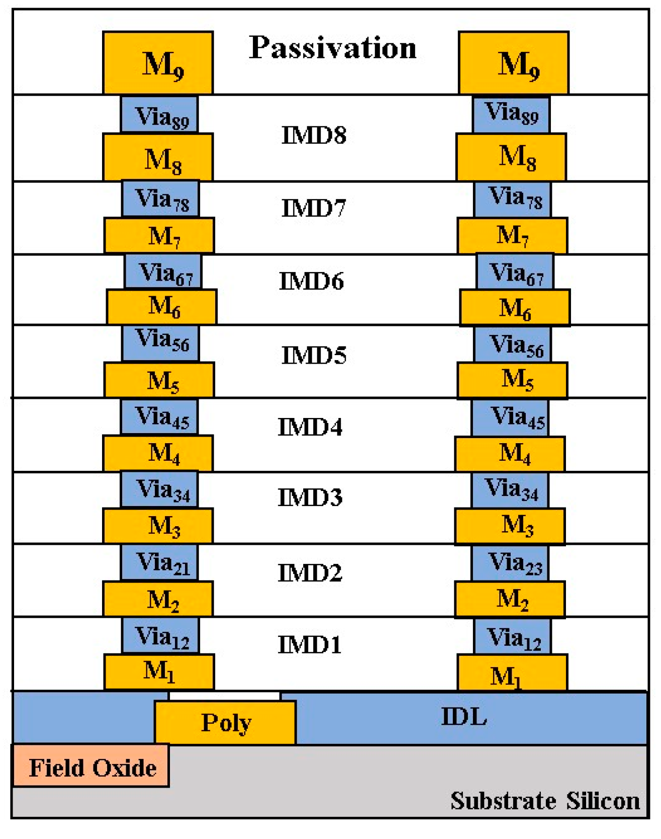
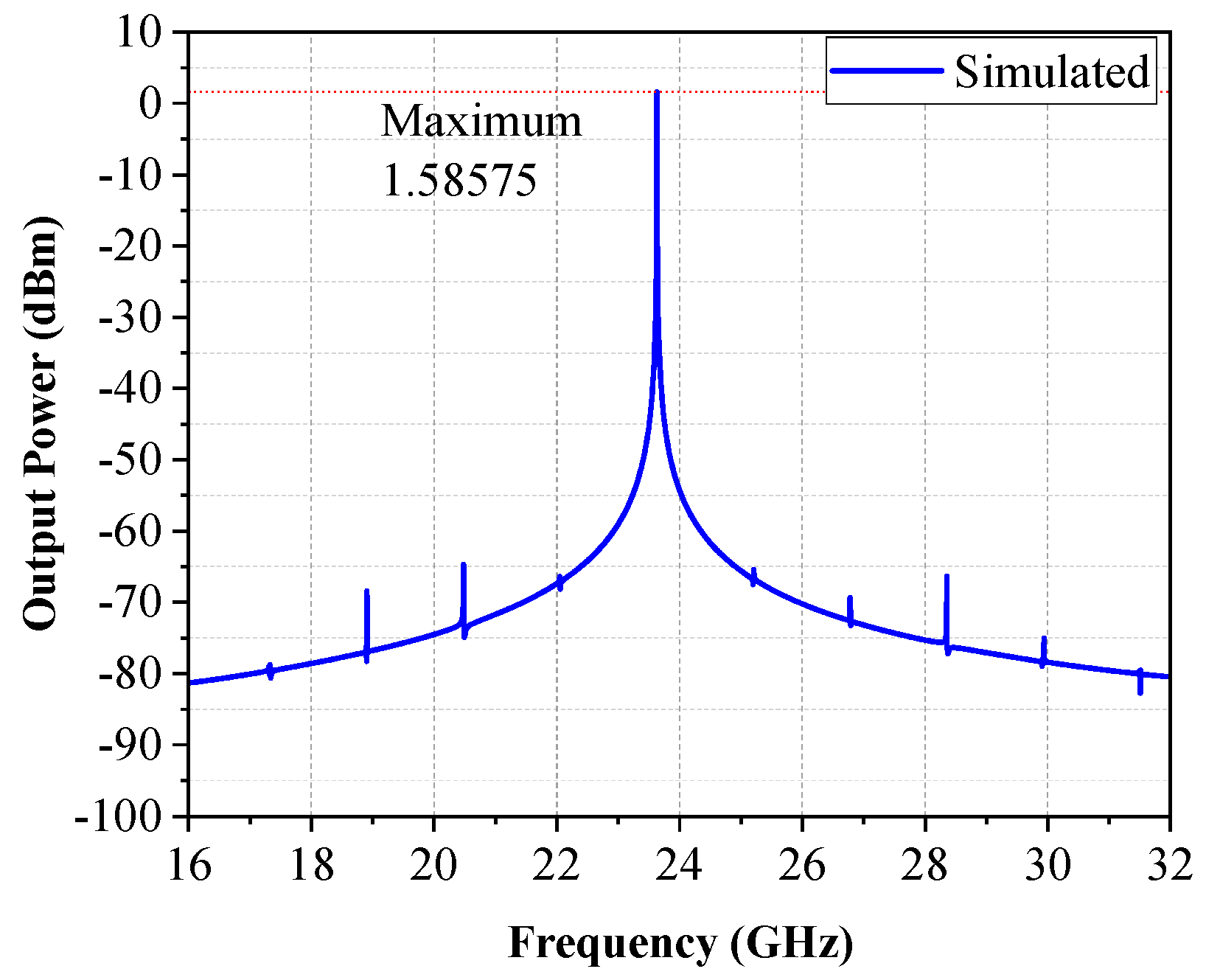
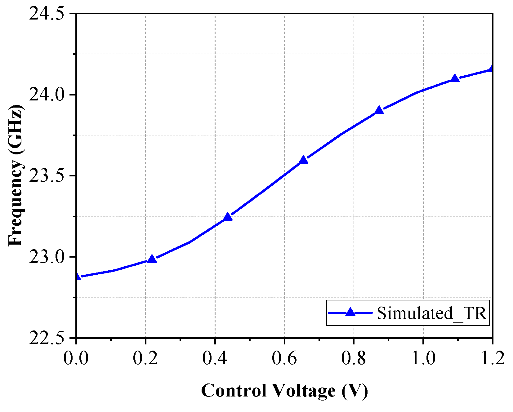
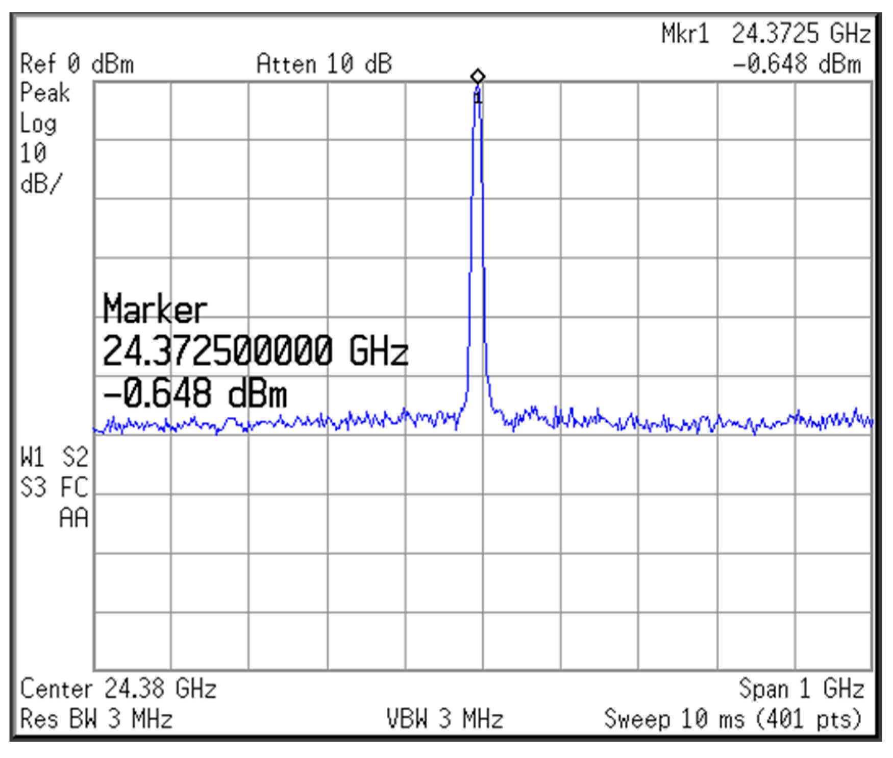
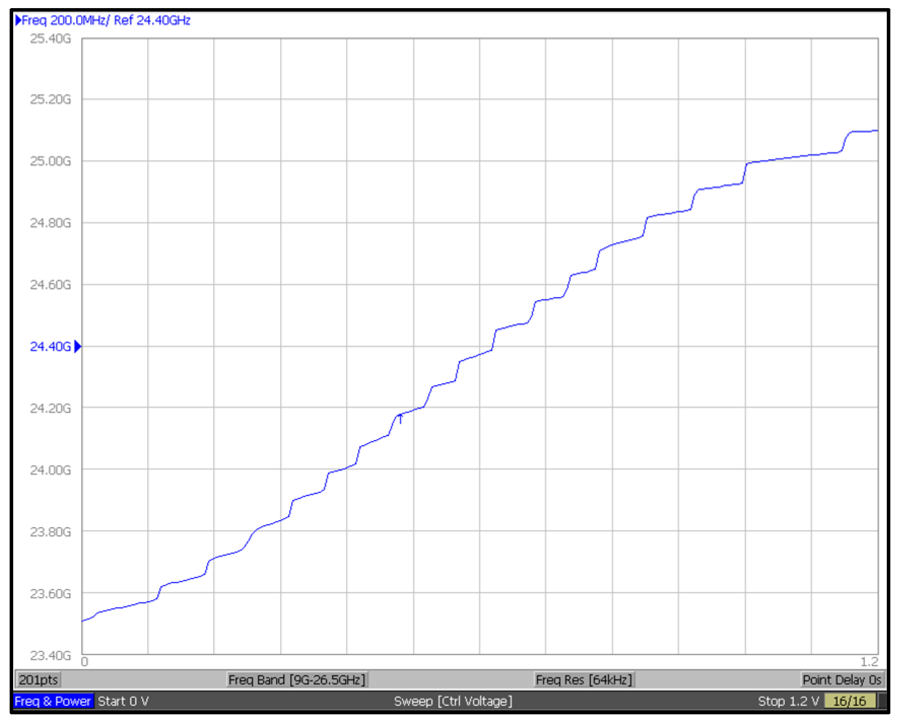
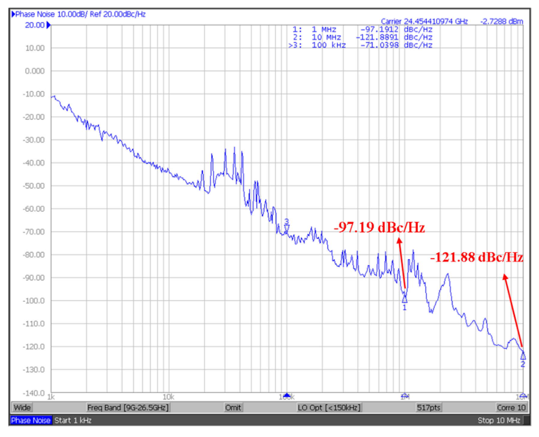
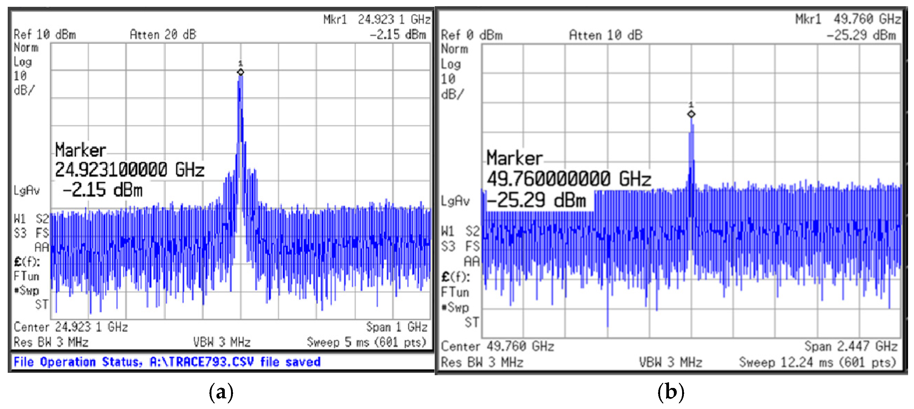
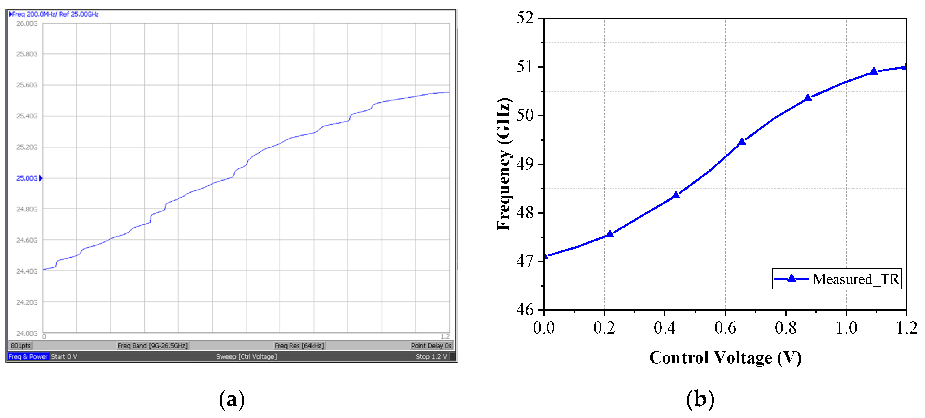
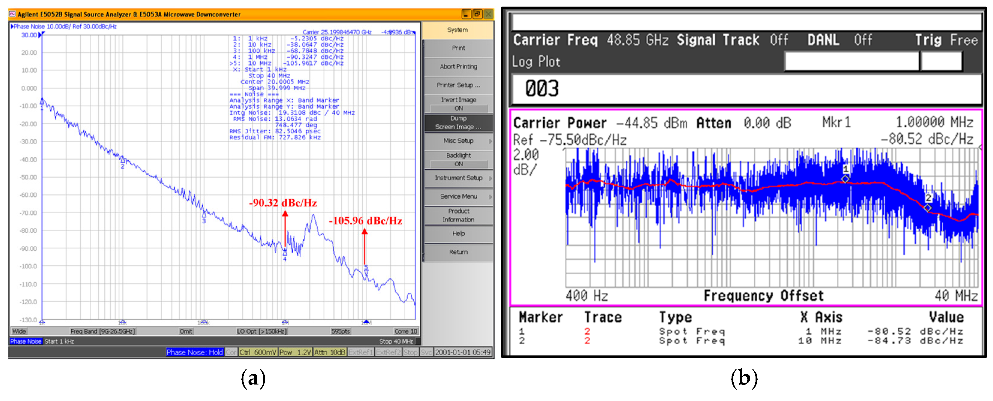
3. Implementation and Experimental Results

Both the two VCOs that the 24-GHz design adds a noise filter to reduce phase noise and the 48-GHz design that uses the push-push architecture are fabricated using the TSMC 90-nm CMOS process. The process provides a single poly layer and nine metal layers (1P9M) for interconnections. The chip size, including RF and DC testing pads of 24-GHz VCO, is 0.68 mm × 0.69 mm, and the push–push VCO is 0.7 mm × 0.7 mm, respectively.
On-wafer measurements were performed to characterize the output spectrum, tuning range and phase noise. For the 24-GHz VCO measurements, two ground-signal-ground (GSG) RF probes were used for differential output at the power supply end, one PGPPGP DC probe for VDD, Vctrl and for the two output buffer gate terminals’ DC supply, and one PGP probe DC probe for the current mirror bias VB. There are bypass capacitors on the DC lines to reduce low-frequency noise, as shown in Figure 8a. As for the 48-GH z push–push VCO, one GSGSG RF probe was used for the 48-GHz output signal, one PGP DC probe for VDD and Vctrl, one PGP DC probe for output buffer gate terminals, and the current mirror bias VB, as shown in Figure 8b.
Figure 9 shows the measured output spectrum of the proposed VCO; the measurement DC current of VCO without buffer is 5.1 mA, 6.12 mW. When Vctrl is 0.6 V, the output frequency of the voltage-controlled oscillator is 24.37 GHz and the output power is −0.65 dBm. Figure 10 shows the measured tuning range of the proposed 24 GHz VCO. When the control voltage Vctrl varies from 0 to 1.2 V and the frequency range is 23.51~25.09 GHz, the tuning range is 6.5%. When measuring the tuning range, we set the control voltage sweep points to 201 points. This will cause the VCO output frequency to change discontinuously when the sweep range is wide. If a higher number of points (such as 801 points) is used for scanning, the curve will become smoother and more continuous. Figure 11 shows the measured phase noise of the proposed 24 GHz VCO; the phase noise measured at a 1 MHz offset is −97.2 dBc/Hz, and that measured at a 10 MHz offset is −121.9 dBc/Hz.
Figure 12 shows the measured output spectrum of the proposed push–push VCO. The measurement DC current of the design without buffers is 5.74 mA, and Pout is 6.89 mW. In Figure 12a, when Vctrl is 0.6 V, the output frequency of the f0 is 24.92 GHz and the output power is −2.15 dBm. In Figure 12b, when Vctrl is 0.6 V, the output frequency of the 2f0 is 49.76 GHz and the output power is −25.29 dBm. Figure 13 shows that the measured tuning range of the push–push VCO. With the control voltage Vctrl varying from 0 to 1.2 V, the frequency range of f0 is 24.1~25.9 GHz and that of 2f0 is 47.1~51 GHz. Figure 14 shows the measured phase noise of the VCO. In Figure 14a,b, the measured phase noises of f0 at a 1 MHz offset and of 2f0 at a 1 MHz offset are −90.32 dBc/Hz and −80.52 dBc/Hz, respectively.
In general, good agreements between the simulated and measured results can be observed. Table 1 summarizes previously reported CMOS VCOs. Among these works, the proposed 24-GHz design features good performances in the output power, power consumption, phase noise and FOM. The simulation and measurement results both show that the overall phase noise can be reduced after adding the noise-filtering circuit. The comparison table of the proposed push–push VCO is shown in Table 2. The proposed 48-GHz design has a high output power, low power consumption and acceptable phase noise performances. Equation (5) explains how the FOM in Table 1 and Table 2 is defined and calculated.
FOM = PN 20 log f OSC   f + 10 log P VCO 1   mW

4. Conclusions

Two low phase noise voltage-controlled oscillators were developed and implemented using CMOS 90-nm process. One is implemented in the 24-GHz frequency band, and the other is based on a push–push topology with a λ/4 transmission line that ranges up to the 48-GHz band. The good agreement between the simulated and measured results demonstrates the feasibility of the design concept. In both circuit architectures, adding the LC filtering technique at the tail current source can effectively reduce circuit phase noise; furthermore, in the push–push VCO, the use of the quarter-wavelength transmission line architecture can effectively reduce power consumption. This paper also proves that the push–push architecture can achieve a high-frequency oscillation in even a standard process, which can be applied to the RF transceiver system in the millimeter wave frequency band and to short-range radar applications to provide stable local signals.

Author Contributions

Conceptualization, C.-C.K.; methodology, C.-C.K.; software, C.-C.K.; validation, C.-C.K.; formal analysis, C.-C.K.; investigation, C.-C.K. and S.W.; resources, S.W.; data curation; writing—original draft preparation, S.W.; writing—review and editing, S.W.; visualization, C.-C.K.; supervision, S.W.; project administration, S.W.; funding acquisition, S.W. All authors have read and agreed to the published version of the manuscript.

Funding

This work is supported by National Taipei University of Technology-King Mongkut’s Institute of Technology Ladkrabang Joint Research Program (NTUT-KMITL No. NTUT-KMITL-112-03) and National Science and Technology Council under NSTC 113-2218-E-A49-020-.

Data Availability Statement

The original contributions presented in the study are included in the article, further inquiries can be directed to the corresponding author.

Conflicts of Interest

The authors declare no conflicts of interest.

References

  1. Hegazi, E.; Sjoland, H.; Abidi, A.A. A filtering technique to lower LC oscillator phase noise. IEEE J. Solid-State Circuits 2001, 36, 1921–1930. [Google Scholar] [CrossRef]
  2. Yang, D.; Zhang, L.; Wang, H.; Zeng, D.; Zhou, C.; Yang, D. A 24GHz low phase noise feedback CMOS LC-VCO. In Proceedings of the 2011 IEEE International Conference of Electron Devices and Solid-State Circuits, Tianjin, China, 17–18 November 2011; pp. 1–2. [Google Scholar]
  3. Fu, Y.; Yao, H.; Dai, Y.; Wu, Y.; Huang, G. A 20GHz LC-VCO for Satellite Microwave Communication Application. In Proceedings of the 2020 IEEE MTT-S International Microwave Workshop Series on Advanced Materials and Processes for RF and THz Applications (IMWS-AMP), Suzhou, China, 29–31 July 2020; pp. 1–4. [Google Scholar]
  4. Lin, C.-H.; Yang, C.-Y. A 17-21GHz Current-Folding Frequency Tripler with >36 dBc Harmonic Rejection in 90nm CMOS. In Proceedings of the 2022 IEEE Asian Solid-State Circuits Conference (A-SSCC), Taipei, Taiwan, 6–9 November 2022; pp. 1–3. [Google Scholar]
  5. Barajas, B.; Molavi, R.; Mirabbasi, S. A Wideband 65-nm 60-GHz Push-Push LC VCO using a Nonlinear Varactor Array. In Proceedings of the 2024 IEEE 67th International Midwest Symposium on Circuits and Systems (MWSCAS), Springfield, MA, USA, 11–14 August 2024; pp. 367–371. [Google Scholar]
  6. Wang, L.; Upadhyaya, P.; Sun, P.; Zhang, Y.; Heo, D.; Chen, Y.J.; Jeong, D.H. A 5.3GHz low-phase-noise LC VCO with harmonic filtering resistor. In Proceedings of the 2006 IEEE International Symposium on Circuits and Systems (ISCAS), Kos, Greece, 21–24 May 2006; p. 4. [Google Scholar]
  7. Katz, A.; Degani, O.; Socher, E. Design and optimization of a low-noise cross-coupled fundamental VCO in 90nm CMOS for 60GHz applications. In Proceedings of the 2011 IEEE 11th Topical Meeting on Silicon Monolithic Integrated Circuits in RF Systems, Glendale, AZ, USA, 17–19 January 2011; pp. 13–16. [Google Scholar]
  8. Luo, J.; He, J.; Wang, H.; Chang, S.; Huang, Q.; Xiong, Y.-Z. A 150-GHz push-push VCO in 0.13-μm SiGe BiCMOS. In Proceedings of the 2014 International Symposium on Integrated Circuits (ISIC), Singapore, 10–12 December 2014; pp. 308–311. [Google Scholar]
  9. Chiang, M.-J.; Wu, H.-S.; Tzuang, C.-K.C. Prorogation Characteristics of CMOS Synthetic Transmission Line and Slow-Wave Inductor on the Complementary Spiral-Shaped Electromagnetic Bandgap (EBG) Shielding Ground Plane. In Proceedings of the 2007 Asia-Pacific Microwave Conference, Bangkok, Thailand, 11–14 December 2007; pp. 1–4. [Google Scholar]
  10. Pawar, S.N.; Mane, P.B. Design and Implementation of KU Band LC-VCO using 90nm CMOS Process. In Proceedings of the 2020 International Conference on Smart Electronics and Communication (ICOSEC), Trichy, India, 10–12 September 2020; pp. 1234–1238. [Google Scholar]
  11. Li, D.; Zhang, L.; Wang, Y. A 60GHz quadrature LO synthesizer with 1.2° phase error and over 17% tuning range for IEEE 802.11ad applications. In Proceedings of the 2014 12th IEEE International Conference on Solid-State and Integrated Circuit Technology (ICSICT), Guilin, China, 28–31 October 2014; pp. 1–3. [Google Scholar]
  12. Huang, L.; Yuan, S.; Zhang, R.; Li, W. A 15 GHz CMOS low phase noise VCO using coupled coplanar waveguide. In Proceedings of the 2011 3rd International Conference on Computer Research and Development, Shanghai, China, 11–13 March 2011; pp. 310–313. [Google Scholar]
  13. Wang, Z.; Jiang, S.; Jiang, H.; Chi, B. A K-Band Fractional-N Frequency Synthesizer with a Low Phase Noise LC VCO in 90nm CMOS. In Proceedings of the 2018 IEEE International Symposium on Circuits and Systems (ISCAS), Florence, Italy, 27–30 May 2018; pp. 1–4. [Google Scholar]
  14. Kwok, K.; Long, J.R.; Pekarik, J.J. A 23-to-29GHz Differentially Tuned Varactorless VCO in 0.13μm CMOS. In Proceedings of the 2007 IEEE International Solid-State Circuits Conference, San Francisco, CA, USA, 11–15 February 2007; Digest of Technical Papers. pp. 194–596. [Google Scholar]
  15. Chang, Y.-H. Low-Voltage Dual-B and CMOS Voltage-Controlled Oscillator for Ka-Band and V-Band Applications. IEEE Microw. Wirel. Compon. Lett. 2021, 31, 1307–1310. [Google Scholar] [CrossRef]
  16. Yu, A.H.-T.; Tam, S.W.; Kim, Y.; Socher, E.; Hant, W.; Chang, M.C.; Itoh, T. A Dual-Band Millimeter-Wave CMOS Oscillator with Left-Handed Resonator. IEEE Trans. Microw. Theory Tech. 2010, 58, 1401–1409. [Google Scholar] [CrossRef]
  17. Chiu, H.-C.; Kao, C.-P. A Wide Tuning Range 69 GHz Push-Push VCO Using 0.18 μm CMOS Technology. IEEE Microw. Wirel. Compon. Lett. 2010, 20, 97–99. [Google Scholar] [CrossRef]
Figure 1. Cross-section of a standard 90-nm CMOS process.
Micromachines 16 00682 g001
Figure 2. Schematic of the proposed CMOS 24 GHz VCO.
Micromachines 16 00682 g002
Figure 3. Simulated output spectrum.
Micromachines 16 00682 g003
Figure 4. Simulation of VCO tuning range.
Micromachines 16 00682 g004
Figure 5. Phase noise comparison chart after adding noise filter circuit.
Micromachines 16 00682 g005
Figure 6. (a) The proposed λ /4 transmission line in CMOS 90-nm process, (b) slow-wave factor (SWF), and (c) attenuation results of 50-Ω λ /4 transmission line.
Micromachines 16 00682 g006
Figure 7. Schematic of the proposed 48 GHz Push-Push VCO.
Micromachines 16 00682 g007
Figure 8. Chip photo of the proposed (a) 24-GHz and (b) 48-GHz push–push VCOs.
Micromachines 16 00682 g008
Figure 9. Measured output spectrum of the proposed 24 GHz VCO.
Micromachines 16 00682 g009
Figure 10. Measured tuning range of the proposed 24 GHz VCO.
Micromachines 16 00682 g010
Figure 11. Measured phase noise of the proposed 24 GHz VCO.
Micromachines 16 00682 g011
Figure 12. Measured output spectrum of the proposed push–push VCO: (a) f0 and (b) 2f0.
Micromachines 16 00682 g012
Figure 13. Measured tuning range of the proposed push–push VCO: (a) f0 and (b) 2f0.
Micromachines 16 00682 g013
Figure 14. Measured phase noise of the proposed push–push VCO: (a) f0 and (b) 2f0.
Micromachines 16 00682 g014
Table 1. Comparison of previously reported CMOS VCOs.
Ref.[12][13][14]This Work
Technology (nm)906513090
Supply (V)1.51.21.21.2
Frequency (GHz)14.62–15.521.4–22.423.2–29.423.51–25.09
Power Consumption (mW)9.131636.56.12
POUT (dBm)−4.12N/A−11−0.65
Tuning Range (%)5.81126.56.5
Phase Noise (dBc/1MHz)−94.86−93.4−92.6−97.19
FOM−168−179.5−165.4−177.1
Chip Core Area (mm2)N/A0.640.120.47
Table 2. Comparison of previously reported push–push or millimeter-wave CMOS VCOs.
Ref.[15][16][17]This Work
Technology (nm)909018090
Supply (V)0.61.21.81.2
Frequency (GHz)28.26/56.5221/5569.324.9/49.8
Power Consumption (mW)7.081427.56.89
POUT (dBm)−13.74/−40.47−30.5/−21.17−31.46−2.15/−25.29
Tuning Range (%)8.83N/A5.27.2
Phase Noise (dBc/1MHz)−95.62/−87.83−100.8/−86.7−75.23−90.32/−80.52
FOM−176.1/−174.3−175.8/−170−158.3−169.9/−166.2
Chip Core Area (mm2)0.420.0090.2080.49
Disclaimer/Publisher’s Note: The statements, opinions and data contained in all publications are solely those of the individual author(s) and contributor(s) and not of MDPI and/or the editor(s). MDPI and/or the editor(s) disclaim responsibility for any injury to people or property resulting from any ideas, methods, instructions or products referred to in the content.

